

Page 1
Global LCD Panel Exchange Center
and comments.
MODEL NO.: V315B5
www.panelook.com
PRODUCT SPECIFICATION
□Tentative Specification
□ Preliminary Specification
■ Approval Specification
SUFFIX:L10
CustomerΚ
APPROVED BY SIGNATURE
Name / Title
Note
Please return 1 copy for your confirmation with your signature
Approved By Checked By Prepared By
Chao-Chun Chung
Josh Chi
Chloe Chen
Version 2.0 1 DateΚΚ11 Jul 2011
The copyright belongs to CHIMEI InnoLux. Any unauthorized use is prohibited
One step solution for LCD / PDP / OLED panel application: Datasheet, inventory and accessory!
www.panelook.com
Page 2
Global LCD Panel Exchange Center
www.panelook.com
PRODUCT SPECIFICATION
CONTENTS -
REVISION HISTORY ------------------------------------------------------- 3
1. GENERAL DESCRIPTION ------------------------------------------------------- 4
1.1 OVERVIEW
1.2 FEATURES
1.3 APPLICATION
1.4 GENERAL SPECIFICATIONS
1.5 MECHANICAL SPECIFICATIONS
2. ABSOLUTE MAXIMUM RATINGS ------------------------------------------------------- 6
2.1 ABSOLUTE RATINGS OF ENVIRONMENT
2.2 PACKAGE STORAGE
2.3 ELECTRICAL ABSOLUTE RATINGS
3. ELECTRICAL CHARACTERISTICS ------------------------------------------------------- 8
3.1 TFT LCD MODULE
3.2 CCFL(Cold Cathode Fluorescent Lamp) CHARACTERISTICS
4. BLOCK DIAGRAM ------------------------------------------------------- 13
4.1 TFT LCD MODULE
5. INTERFACE PIN CONNECTION ------------------------------------------------------- 14
5.1 TFT LCD MODULE
5.2 BACKLIGHT UNIT
5.3 T-BALANCE BOARD UNIT
5.4 BLOCK DIAGRAM OF INTERFACE
5.5 LVDS INTERFACE
5.6 COLOR DATA INPUT ASSIGNMENT
6. INTERFACE TIMING ------------------------------------------------------- 21
6.1 INPUT SIGNAL TIMING SPECIFICATIONS
6.2 POWER ON/OFF SEQUENCE
7. OPTICAL CHARACTERISTICS ------------------------------------------------------- 25
7.1 TEST CONDITIONS
7.2 OPTICAL SPECIFICATIONS
8. DEFINITION OF LABELS ------------------------------------------------------- 31
8.1 CMI MODULE LABEL
9. PACKAGING ------------------------------------------------------- 32
9.1 PACKING SPECIFICATIONS
9.2 PACKING METHOD
10. PRECAUTIONS ------------------------------------------------------- 34
10.1 ASSEMBLY AND HANDLING PRECAUTIONS
10.2 SAFETY PRECAUTIONS
11. MECHANICAL CHARACTERISTICS ------------------------------------------------------- 35
Version 2.0 2 DateΚΚ11 Jul 2011
The copyright belongs to CHIMEI InnoLux. Any unauthorized use is prohibited
One step solution for LCD / PDP / OLED panel application: Datasheet, inventory and accessory!
www.panelook.com
Page 3
Global LCD Panel Exchange Center
www.panelook.com
PRODUCT SPECIFICATION
Version
Ver 2.0
Date
Jul 11, 11’
’
Page
(New)
All
Section
All
REVISION HISTORY
Description
Approval Specification was first issued.
Version 2.0 3 DateΚΚ11 Jul 2011
The copyright belongs to CHIMEI InnoLux. Any unauthorized use is prohibited
One step solution for LCD / PDP / OLED panel application: Datasheet, inventory and accessory!
www.panelook.com
Page 4
Global LCD Panel Exchange Center
1. GENERAL DESCRIPTION
1.1 OVERVIEW
V315B5- L10 s a 31.5” TFT Liquid Crystal Display module with 4U-type CCFL backlight unit and
1ch-LVDS interface. This module supports 1366 x 768 WXGA format and can display 16.7M
(8-bit/color)colors. The T-balance board module for backlight is built-in.
1.2 FEATURES
- High brightness (450 nits)
- Ultra-high contrast ratio (3500:1)
- Fast response time (gray to gray average 8.5ms)
- Fast response time (8.5ms)
- High color saturation NTSC 72%
www.panelook.com
PRODUCT SPECIFICATION
- HDTV (1366 x 768 pixels) resolution, WXGA format
- Ultra wide viewing angle : 176(H)/176(V)(CR≥20)with Super MVA technology
- DE (Data Enable) only mode
- LVDS (Low Voltage Differential Signaling) interface
- Optimized response time for 60Hz frame rate
- RoHs compliance
- Color reproduction (nature color)
- Low color shift function
1.3 APPLICATION
- TFT LCD TVs
- Multi-Media Display
1.4 GENERAL SPECIFICATI0NS
Item Specification Unit Note
Active Area 697.6845 (H) x 392.256 (V) (31.51" diagonal) mm
Bezel Opening Area 703.8 (H) x 399.0 (V) mm
Driver Element a-si TFT active matrix -
Pixel Number 1366 x R.G.B. x 768 pixel
Pixel Pitch (Sub Pixel) 0.17025(H) x 0.51075 (V) mm
Pixel Arrangement RGB vertical stripe -
Power consumption
Display Colors 16.7M color
Display Operation Mode Transmissive mode / Normally black -
Surface Treatment Anti-Glare coating (Haze 11%),Hard coating (3H)
Note (1) Please refer to the attached drawings in sec 11 for more information about the front and back outlines.
74 W
-
(1)
(2)
(3)
Note (2) Please refer sec 3.1 and 3.2 for more information of Power consumption
Note (3) The spec. of the surface treatment is temporarily for this phase. CMI reserves the rights to change this
feature.
Version 2.0 4 DateΚΚ11 Jul 2011
The copyright belongs to CHIMEI InnoLux. Any unauthorized use is prohibited
One step solution for LCD / PDP / OLED panel application: Datasheet, inventory and accessory!
www.panelook.com
Page 5
Global LCD Panel Exchange Center
1.5 MECHANICAL SPECIFICATIONS
Item Min. Typ. Max. Unit Note
Horizontal(H) 759 760 761 mm (1)
Module Size
Note (1) Please refer to the attached drawings for more information of front and back outline dimensions.
Note (2) Module Depth is between bezel to T-CON cover.
Note (3) Module Depth is between bezel to Inverter cover.
Vertical(V) 449 450 451 mm (1)
Depth(D) 31.5 32.5 33.5 mm (2)
Depth(D) 53.8 54.8 55.8 mm
Weight 5219 g
www.panelook.com
PRODUCT SPECIFICATION
(3)
Version 2.0 5 DateΚΚ11 Jul 2011
The copyright belongs to CHIMEI InnoLux. Any unauthorized use is prohibited
One step solution for LCD / PDP / OLED panel application: Datasheet, inventory and accessory!
www.panelook.com
Page 6
Global LCD Panel Exchange Center
2. ABSOLUTE MAXIMUM RATINGS
2.1 ABSOLUTE RATINGS OF ENVIRONMENT
Item Symbol
Storage Temperature TST -20 +60 ºC (1)
Operating Ambient Temperature TOP 0 +50 ºC (1), (2)
Shock (Non-Operating) S
Vibration (Non-Operating) V
Note (1) Temperature and relative humidity range is shown in the figure below.
(a) 90 %RH Max. (Ta 40 ºCЉ ).
(b) Wet-bulb temperature should be 39 ºC Max. (Ta > 40 ºC).
(c) No condensation.
Note (2) The maximum operating temperature is based on the test condition that the surface temperature of
display area is less than or equal to 65 ºC with LCD module alone in a temperature controlled chamber.
www.panelook.com
PRODUCT SPECIFICATION
Value
Min. Max.
- 50 G (3), (5)
NOP
- 1.0 G (4), (5)
NOP
Unit Note
Thermal management should be considered in final product design to prevent the surface temperature of
display area from being over 65 ºC. The range of operating temperature may degrade in case of improper
thermal management in final product design.
Note (3) 11 ms, half sine wave, 1 time for ± X, ± Y, ± Z.
Note (4) 10 ~ 200 Hz, 10 min, 1 time each X, Y, Z.
Note (5) At testing Vibration and Shock, the fixture in holding the module has to be hard and rigid enough so
that the module would not be twisted or bent by the fixture.
Relative Humidity (%RH)
100
90
80
60
Operating Range
40
20
10
Storage Range
Temperature (ºC)
Version 2.0 6 DateΚΚ11 Jul 2011
The copyright belongs to CHIMEI InnoLux. Any unauthorized use is prohibited
One step solution for LCD / PDP / OLED panel application: Datasheet, inventory and accessory!
80 60 -20 40 0 20 -40
www.panelook.com
Page 7
Global LCD Panel Exchange Center
2.2 PACKING STORAGE
When storing modules as spares for a long time, the following precaution is necessary.
(a) Do not leave the module in high temperature, and high humidity for a long time. It is highly recommended to
store the module with temperature from 0 to 35 at normal humidity without condensation.к
(b)The module shall be stored in dark place. Do not store the TFT-LCD module in direct sunlight or fluorescent
light.
2.3 ELECTRICAL ABSOLUTE RATINGS
2.3.1 TFT LCD MODULE
Item Symbol
Power Supply Voltage Vcc -0.3 13.5 V
Input Signal Voltage VIN -0.3 3.6 V
www.panelook.com
PRODUCT SPECIFICATION
Value
Min. Max.
Unit Note
(1)
2.3.2 BACKLIGHT UNIT
Ё
Value
3000
15
Item Symbol
Lamp Voltage
Power Supply Voltage
Control Signal Level
Note (1) Permanent damage to the device may occur if maximum values are exceeded. Functional operation
should be restricted to the conditions described under normal operating conditions.
Note (2) No moisture condensation or freezing.
Note (3)The control signals include On/Off Control, External PWM Control and DET_5V signal for inverter status
output.
V
High / Low
Ё
Min. Max.
195 (Low) 390 (High) Vrms
-0.3
Unit Note
V
RMS
(1)
V
(1), (3)
Version 2.0 7 DateΚΚ11 Jul 2011
The copyright belongs to CHIMEI InnoLux. Any unauthorized use is prohibited
One step solution for LCD / PDP / OLED panel application: Datasheet, inventory and accessory!
www.panelook.com
Page 8
Global LCD Panel Exchange Center
www.panelook.com
PRODUCT SPECIFICATION
3. ELECTRICAL CHARACTERISTICS
3.1 TFT LCD MODULE
Ta = 25 ± 2 ºC
Value
Parameter Symbol
Min. Typ. Max.
Power Supply Voltage VCC 10.8 12 13.2 V (1)
Unit Note
Rush Current I
White Pattern PT 6.72 8.28 W
Power consumption
Power Supply
Current
Differential Input High
Threshold Voltage
Differential Input Low
LVDS
interface
CMOS
Threshold Voltage
Common Input Voltage VCM 1.0 1.2 1.4 V
Differential input voltage
(single-end)
Terminating Resistor RT
Input High Threshold
Voltage
Black Pattern PT 5.28 6.24 W
Horizontal Stripe P
White Pattern
Black Pattern
Horizontal
Stripe
RUSH
T
᧩ ᧩
᧩ ᧩
᧩ ᧩
V
LVT H
V
LVT L
|VID|
VIH 2.7
᧩ ᧩
᧩
+100
᧩ ᧩
200
᧩
7.68 9.24 W
0.56 0.69 A
0.44 0.52 A
0.64 0.77 A
᧩ ᧩
᧩
100
᧩
2.8 A
mV
-100 mV
600 mV
᧩
3.3 V
ohm
(2)
(3)
(4)
interface
Input Low Threshold
Voltage
VIL 0
᧩
0.7 V
Note (1) The module should be always operated within above ranges.
Note (2) Measurement Conditions:
Version 2.0 8 DateΚΚ11 Jul 2011
The copyright belongs to CHIMEI InnoLux. Any unauthorized use is prohibited
One step solution for LCD / PDP / OLED panel application: Datasheet, inventory and accessory!
www.panelook.com
Page 9
Global LCD Panel Exchange Center
www.panelook.com
PRODUCT SPECIFICATION
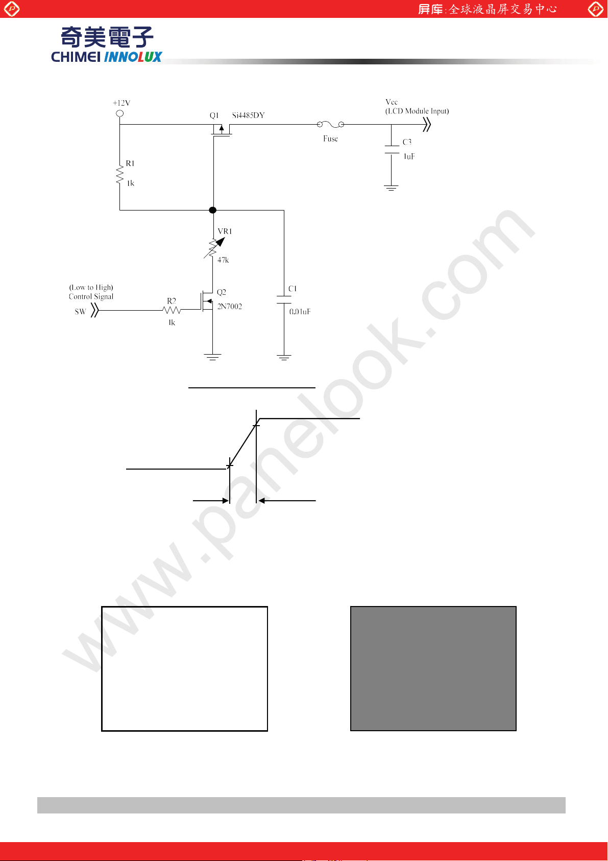
Vcc rising time is 470us
+12V
0.9Vcc
0.1Vcc
GND
470us
Note (3) The specified power supply current and power consumption is under the conditions at Vcc = 12 V,
Ta = 25 ± 2 ºC, f
= 60 Hz, whereas a power dissipation check pattern below is displayed.
v
a. White Pattern
b. Black Pattern
Active Area
Active Area
Version 2.0 9 DateΚΚ11 Jul 2011
The copyright belongs to CHIMEI InnoLux. Any unauthorized use is prohibited
One step solution for LCD / PDP / OLED panel application: Datasheet, inventory and accessory!
www.panelook.com
Page 10
Global LCD Panel Exchange Center
c. Horizontal Pattern
Note (4) The LVDS input characteristics are as follows:
www.panelook.com
PRODUCT SPECIFICATION
/9'6
/9'6
_9,'_
/9'6
9&0
*1'
_9,'_
9
Version 2.0 10 DateΚΚ11 Jul 2011
The copyright belongs to CHIMEI InnoLux. Any unauthorized use is prohibited
One step solution for LCD / PDP / OLED panel application: Datasheet, inventory and accessory!
www.panelook.com
Page 11
Global LCD Panel Exchange Center
www.panelook.com
PRODUCT SPECIFICATION
3.2 CCFL (Cold Cathode Fluorescent Lamp) CHARACTERISTICS
3.2.1 CCFL (Cold Cathode Fluorescent Lamp) CHARACTERISTICS (Ta = 25 ± 2 ºC)
Parameter Symbol
Min. Typ. Max.
Lamp Input Voltage VL - 1560 Lamp Current IL 11.8 12.3 12.8
Lamp Turn On Voltage
VS
- -
- Operating Frequency FL 40 - 80 KHz
Lamp Life Time LBL 50,000 - - Hrs (4)
3.2.2 T-BALANCE BOARD CHARACTERISTICS (Ta = 25 ± 2 ºC)
Value
2710
2260
Unit Note
V
RMS
mA
RMS
V
Ta = 0 ºC (2)
RMS
Ta = 25 ºC (2)
V
RMS
(1)
(3)
Parameter Symbol
Unit Note
Min. Typ. Max.
Value
Input High Voltage High
Input Low Voltage Low
Protection Circuit Supply
Voltage
Vcc
Power Consumption PIP - 74 78 W
Input Current ITB 0.19 0.2 Arms
F
Oscillating Frequency
61 63 65 kHz
W
380 390 400 Vrms
190 195 200 V
11 13 15
V
No Dimming
(IPB input)
Measure TBB
HIGH(390V)
Individual Lamp Current IL 11.3 12.3 13.3 mA (5)
Connector
Detection
All Lamp Open
Detection
One Lamp
Open Detection
High CNTPRT
Vcc-0.5
Low CNTPRT
High LD
Vcc-0.5
Low LD
High OVP
Low OVP
-
-
1.25
0
- Vcc
- 1
- Vcc
- 1
- -
- 0.8
V Normal Operation
V Input Connector Open
V Normal Operation
V All Lamp Open
V Normal Operation
V One Lamp Open
Dimming frequency FB 140 150 160 Hz
(6)
Minimum Duty Ratio D
Striking time tsriking
12 15 18 % (8)
MIN
1
-
2 sec
Shutdown time Tsd 1 1.5 2 sec
Note (1) Lamp current is measured by utilizing AC current probe and its value is average by measuring
master and slave board.:
Note (2) The lamp starting voltage V
should be applied to the lamp for more than 1 second after startup.
S
Otherwise the lamp may not be turned on.
Note (3) The lamp frequency may produce interference with horizontal synchronous frequency of the
display input signals, and it may result in line flow on the display. In order to avoid interference, the
lamp frequency should be detached from the horizontal synchronous frequency and its harmonics
Version 2.0 11 DateΚΚ11 Jul 2011
The copyright belongs to CHIMEI InnoLux. Any unauthorized use is prohibited
One step solution for LCD / PDP / OLED panel application: Datasheet, inventory and accessory!
www.panelook.com
Page 12
Global LCD Panel Exchange Center
as far as possible.
Note (4) The life time of a lamp is defined as when the brightness is larger than 50% of its original value and
the effective discharge length is longer than 80% of its original length (Effective discharge length is
defined as an area that has equal to or more than 70% brightness compared to the brightness at the
center point of lamp.) as the time in which it continues to operate under the condition at Ta = 25
www.panelook.com
PRODUCT SPECIFICATION
±2к and I
= 11.3~13.3 mArms.
L
Note (5) Lamp current is measured master board by utilizing high frequency current meters as shown below:
Note (6) Input voltage Hv based on spec. +-7% tolerance.
Note (7) Asymmetric ratio must be from 90% to 110% (0.9<Ip/ I
rms@T/2X√2
<1.1)
Note (8) The minimum dimming 0% operation should cause flicker by protection circuit.
T
Ip
I-p
HV +(-)
1
Balance
Board
A
2
A
A
1
2
A
1
A
2
A
1
A
2
A
HV -(+)
HV +(-)
HV -(+)
HV +(-)
HV -(+)
HV +(-)
HV -(+)
LCD Module
Version 2.0 12 DateΚΚ11 Jul 2011
The copyright belongs to CHIMEI InnoLux. Any unauthorized use is prohibited
One step solution for LCD / PDP / OLED panel application: Datasheet, inventory and accessory!
www.panelook.com
Page 13

Global LCD Panel Exchange Center
SCAN DRIVER IC
INPUT CONNECTOR
or equal
GND
FRAME BUFFER
RXCLK(+/
-)
SELLVDS
4. BLOCK DIAGRAM
4.1 TFT LCD MODULE
RX0(+/-)
RX1(+/-)
RX2(+/-)
RX3(+/-)
Vcc
Yeonho , 10031HR-30)
High
Low
Gnd
OVP
CNT_PRT
12V
LD
CN1
Balance Board CONNECTOR
CN1: 20037WR-H1224567 (Yeon-Ho )
www.panelook.com
PRODUCT SPECIFICATION
TIMING CONTROLLER
DC/DC CONVERTER &
REFERENCE VOLTAGE
TFT LCD PANEL
(1366x3x768)
DATA DRIVER IC
BACKLIGHT
UNIT
Version 2.0 13 DateΚΚ11 Jul 2011
One step solution for LCD / PDP / OLED panel application: Datasheet, inventory and accessory!
The copyright belongs to CHIMEI InnoLux. Any unauthorized use is prohibited
www.panelook.com
Page 14

Global LCD Panel Exchange Center
Pin No.
Symbol
Description
Note
1 NC No connection
(3)
2 SCL EEPROM Serial Clock
3 SDA
EEPROM Serial Data
4 GND
Ground
5 RX0-
Negative transmission data of pixel 0
6 RX0+
Positive transmission data of pixel 0
7 GND
Groun
d
8 RX1-
Negative transmission data of pixel 1
9 RX1+
Positive transmission data of pixel 1
10 GND
Ground
11 RX2-
Negative transmission data of pixel 2
12 RX2+
Positive transmission data of pixel 2
13 GND
Ground
14 RXCLK
- Negative of clock
15 RXCLK+
Positive of clock
16 GND
Ground
17 RX3-
Negative transmission data of pixel 3
18 RX3+
Positive transmission data of pixel 3
19 GND
Ground
20 NC No connection
(3)
21 SELLVDS
Select LVDS data format
(2)(4)
22 WP EEPROM Write Protection
23 GND
Ground
24 GND
Ground
25 GND
Ground
26 VCC
Power supply: +12V
27 VCC
Power supply: +12V
28 VCC
Power supply: +12V
29 VCC
Power supply: +12V
30 VCC
Power supply: +12V
5. INTERFACE PIN CONNECTION
5.1 TFT LCD MODULE
CNF1 Connector Pin Assignment
www.panelook.com
PRODUCT SPECIFICATION
Note (1) Connector type: 10031HR-30 (Yeonho) or compatible
LVDS connector pin orderdefined as follows
Note (2) Low = Open or connect to GND: JEIDA Format, High = Connect to +3.3V: VESA Format.
Note (3) Reserved for internal use. Please leave it open.
Note (4) LVDS signal pin connected to the LCM side has the following diagram. R1 in the system side should be
less than 1K Ohm. (R1 < 1K Ohm)
Version 2.0 14 DateΚΚ11 Jul 2011
The copyright belongs to CHIMEI InnoLux. Any unauthorized use is prohibited
One step solution for LCD / PDP / OLED panel application: Datasheet, inventory and accessory!
www.panelook.com
Page 15

Global LCD Panel Exchange Center
www.panelook.com
PRODUCT SPECIFICATION
Version 2.0 15 DateΚΚ11 Jul 2011
The copyright belongs to CHIMEI InnoLux. Any unauthorized use is prohibited
One step solution for LCD / PDP / OLED panel application: Datasheet, inventory and accessory!
www.panelook.com
Page 16

Global LCD Panel Exchange Center
5.2 BACKLIGHT UNIT
The pin configuration for the housing and leader wire is shown in the table below.
CN2-CN5 (Socket Connector): E01B-KCF or equivalent
Pin No. Symbol Description
1 HV High Voltage
HV High Voltage
Note (1) The backlight interface housing for high voltage side is a model E01B-KCF, manufactured by JST or
www.panelook.com
PRODUCT SPECIFICATION
Remark
equivalent
.
Version 2.0 16 DateΚΚ11 Jul 2011
The copyright belongs to CHIMEI InnoLux. Any unauthorized use is prohibited
One step solution for LCD / PDP / OLED panel application: Datasheet, inventory and accessory!
www.panelook.com
Page 17

Global LCD Panel Exchange Center
5.3 T-BALANCE BOARD UNIT
CN1(Header): 20037WR-H1224567(Yeon-Ho )
www.panelook.com
PRODUCT SPECIFICATION
Pin № Signal name
1 HIGH (FET) Pulse 390V (Drive, Primary)
2 No pin NC
3 LOW (FET) Blocking (195Vdc, Primary)
4 No pin
5 No pin
6 No Pin NC
7 No Pin NC
8 GND Ground ( Secondary)
9 OVP One Lamp Open Protection
Open Input Connector Protection
10 CNT_PRT
(Normal 12V, Active Low)
11 12V VCC
All Lamp Open Protection
12 LD
(Normal 12V, Active Low)
Feature
NC
NC
Version 2.0 17 DateΚΚ11 Jul 2011
The copyright belongs to CHIMEI InnoLux. Any unauthorized use is prohibited
One step solution for LCD / PDP / OLED panel application: Datasheet, inventory and accessory!
www.panelook.com
Page 18

Global LCD Panel Exchange Center
R0-R7
G0-G7
TxIN
PLL
PLL
R0-R7
Rx0+
Rx0-
Rx1+
Rx2
-
CLK+
Rx
51Ө
51Ө
51Ө
51Ө
51Ө
51Ө
51Ө
51Ө
51Ө
100pF
5.4 BLOCK DIAGRAM OF INTERFACE
www.panelook.com
PRODUCT SPECIFICATION
CNF1
100pF
B0-B7
DE
Rx1-
Rx2+
Rx3+
Rx3-
51Ө
100pF
100pF
G0-G7
B0-B7
DE
Host
Graphics
Controller
Tvd
CLK-
100pF
LVDS Receiver
THC63LVDF84A
DCLK
Timing
Controller
R0~R7 : Pixel R Data
G0~G7 : Pixel G Data
B0~B7 : Pixel B Data
DE : Data Enable Signal
DCLK : Data clock signal
Note (1) The system must have the transmitter to drive the module.
Note (2) LVDS cable impedance shall be 50 ohms per signal line or about 100 ohms per twist-pair line when it is
used differentially
.
Version 2.0 18 DateΚΚ11 Jul 2011
The copyright belongs to CHIMEI InnoLux. Any unauthorized use is prohibited
One step solution for LCD / PDP / OLED panel application: Datasheet, inventory and accessory!
www.panelook.com
Page 19

Global LCD Panel Exchange Center
5.5LVDS INTERFACE
VESA LVDS formatΚ(SELLVDS pin=H)
JEIDA LVDS formatΚ(SELLVDS pin= L or open)
www.panelook.com
PRODUCT SPECIFICATION
R0~R7: Pixel R Data (7; MSB, 0; LSB)
G0~G7: Pixel G Data (7; MSB, 0; LSB)
B0~B7: Pixel B Data (7; MSB, 0; LSB)
DE : Data enable signal
Notes(1) RSVD(reserved)pins on the transmitter shall be “H” or( “L” or OPEN)
Version 2.0 19 DateΚΚ11 Jul 2011
The copyright belongs to CHIMEI InnoLux. Any unauthorized use is prohibited
One step solution for LCD / PDP / OLED panel application: Datasheet, inventory and accessory!
www.panelook.com
Page 20

Global LCD Panel Exchange Center
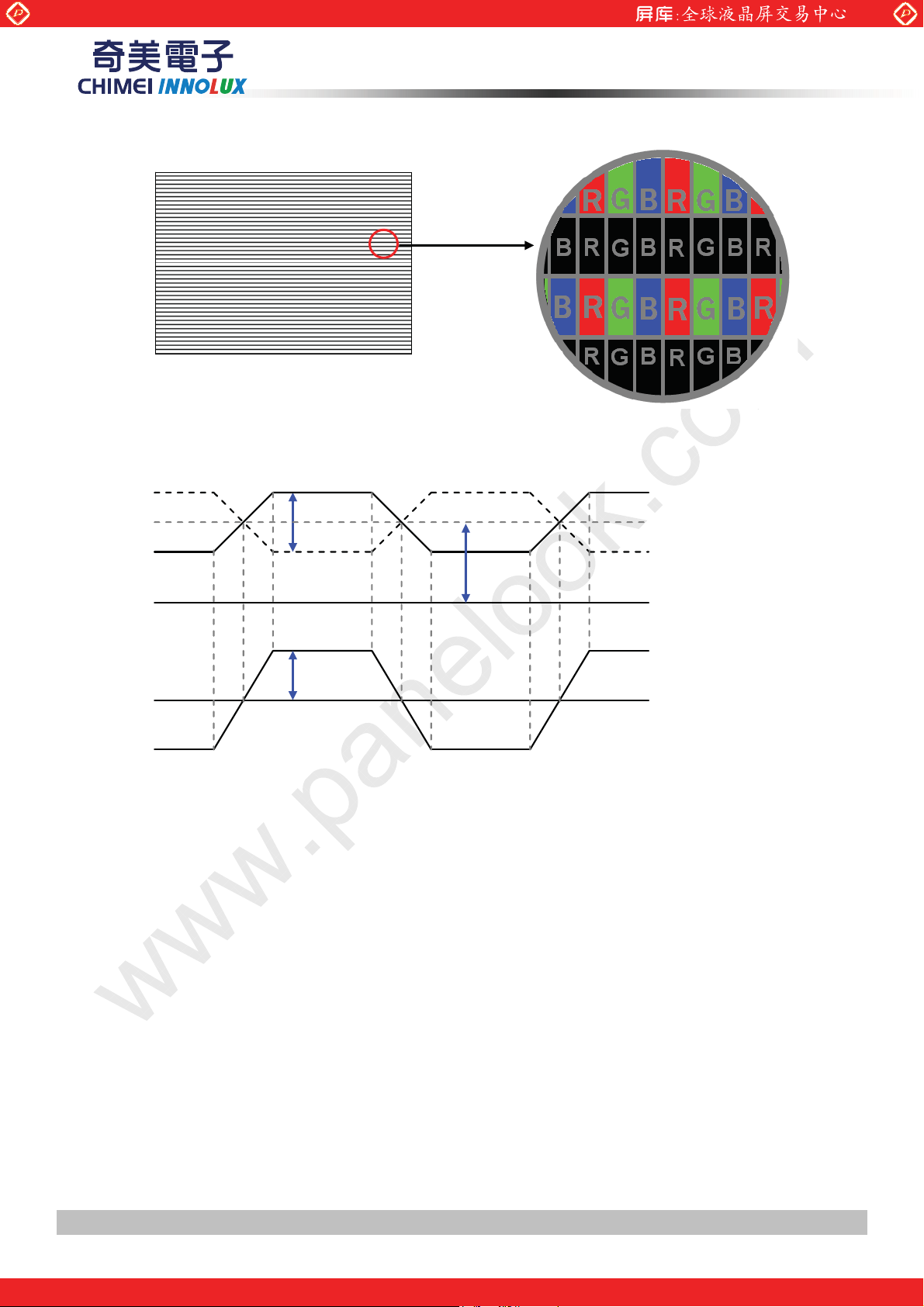
R6 R5 R4 R3 R2 R1 R0 G7 G6 G5 G4 G3 G2 G1 G0 B7 B6 B5 B4 B3 B2 B1 B0
www.panelook.com
PRODUCT SPECIFICATION
5.6 COLOR DATA INPUT ASSIGNMENT
The brightness of each primary color (red, green and blue) is based on the 8-bit gray scale data input for the color.
The higher the binary input, the brighter the color. The table below provides the assignment of the color versus data
input.
Data Signal
Color
R7
Black
Red
Green
Basic
Colors
Gray
Scale
Of
Red
Gray
Scale
Of
Green
Gray
Scale
Of
Blue
Blue
Cyan
Magenta
Yellow
White
Red(0) / Dark
Red(1)
Red(2)
:
:
Red(253)
Red(254)
Red(255)
Green(0) / Dark
Green(1)
Green(2)
:
:
Green(253)
Green(254)
Green(255)
Blue(0) / Dark
Blue(1)
Blue(2)
:
:
Blue(253)
Blue(254)
Blue(255)
Note (1) 0: Low Level Voltage, 1: High Level Voltage
0
0
1
1
0
0
0
0
0
0
1
1
1
1
1
1
0
0
0
0
0
0
:
:
:
:
1
1
1
1
1
1
0
0
0
0
0
0
:
:
:
:
0
0
0
0
0
0
0
0
0
0
0
0
:
:
:
:
0
0
0
0
0
0
Red Green Blue
0
0
0
0
0
0
0
0
0
0
0
0
0
0
0
0
0
0
0
0
0
1
1
1
1
1
1
0
0
0
0
0
0
0
0
0
0
0
0
0
0
0
0
0
0
0
0
0
1
1
1
1
1
1
1
1
0
0
0
0
0
0
0
0
0
0
0
0
0
0
0
0
0
0
0
0
0
1
1
1
1
1
1
1
0
0
0
0
0
0
1
1
1
1
1
1
1
1
1
1
1
1
1
1
1
1
1
1
1
1
1
0
0
0
0
0
0
0
0
1
1
1
1
1
1
1
1
1
1
1
1
1
1
1
1
1
1
1
1
1
0
0
0
0
0
0
0
1
1
1
1
1
1
1
1
1
1
1
1
1
1
1
1
1
1
1
1
1
0
0
0
0
0
0
0
0
0
0
0
0
0
0
0
0
0
0
0
0
0
0
0
0
0
0
1
0
0
0
0
0
0
0
0
0
0
0
0
0
0
0
0
0
0
0
1
0
0
0
0
0
0
0
0
0
0
0
0
0
0
0
0
:
:
:
:
:
:
:
:
:
:
:
:
:
:
:
:
:
:
:
:
:
:
:
:
:
:
:
:
:
:
:
:
:
:
:
:
:
:
:
:
:
:
1
1
1
1
0
1
0
0
0
0
0
0
0
0
0
0
0
0
0
0
0
1
1
1
1
1
0
0
0
0
0
0
0
0
0
0
0
0
0
0
0
0
1
1
1
1
1
1
0
0
0
0
0
0
0
0
0
0
0
0
0
0
0
0
0
0
0
0
0
0
0
0
0
0
0
0
0
0
0
0
0
0
0
0
0
0
0
0
0
0
0
0
0
0
0
0
0
1
0
0
0
0
0
0
0
0
0
0
0
0
0
0
0
0
0
0
0
1
0
0
0
0
0
0
0
0
:
:
:
:
:
:
:
:
:
:
:
:
:
:
:
:
:
:
:
:
:
:
:
:
:
:
:
:
:
:
:
:
:
:
:
:
:
:
:
:
:
:
0
0
0
0
0
0
1
1
1
1
1
1
0
1
0
0
0
0
0
0
0
0
0
0
0
0
0
1
1
1
1
1
1
1
0
0
0
0
0
0
0
0
0
0
0
0
0
0
1
1
1
1
1
1
1
1
0
0
0
0
0
0
0
0
0
0
0
0
0
0
0
0
0
0
0
0
0
0
0
0
0
0
0
0
0
0
0
0
0
0
0
0
0
0
0
0
0
0
0
0
0
0
0
0
0
0
0
0
0
0
0
0
0
0
0
0
0
0
0
0
0
0
0
0
0
1
:
:
:
:
:
:
:
:
:
:
:
:
:
:
:
:
:
:
:
:
:
:
:
:
:
:
:
:
:
:
:
:
:
:
:
:
:
:
:
:
:
:
0
0
0
0
0
0
0
0
0
0
0
0
0
0
1
1
1
1
1
1
0
0
0
0
0
0
0
0
0
0
0
0
0
0
0
1
1
1
1
1
1
1
0
0
0
0
0
0
0
0
0
0
0
0
0
0
1
1
1
1
1
1
1
0
0
0
1
1
1
0
1
0
0
0
:
:
0
0
0
0
0
0
:
:
0
0
0
0
1
0
:
:
1
0
1
Version 2.0 20 DateΚΚ11 Jul 2011
The copyright belongs to CHIMEI InnoLux. Any unauthorized use is prohibited
One step solution for LCD / PDP / OLED panel application: Datasheet, inventory and accessory!
www.panelook.com
Page 21

Global LCD Panel Exchange Center
www.panelook.com
PRODUCT SPECIFICATION
6. INTERFACE TIMING
6.1 INPUT SIGNAL TIMING SPECIFICATIONS (Ta = 25 ± 2 ºC)
The input signal timing specifications are shown as the following table and timing diagram.
Signal Item Symbol
Frequency
Input cycle to
LVDS
cycle jitter
Receiver
Spread spectrum
Clock
modulation range
Spread spectrum
modulation frequency
LVDS
Setup Time Tlvsu 600
Receiver
Data
Vertical
Active
Hold Time Tlvhd 600
Frame Rate
Total Tv 776 806 1018 Th Tv=Tvd+Tvb
Display
Te rm
Display Tvd 768 768 768 Th
Min. Typ. Max. Unit Note
F
clkin
60 76 82 MHz
(=1/TC)
T
clkin_mod
F
F
SSM
rcl
Ё Ё
F
-2%
clkin
Ё
200 ps (3)
+2%
F
clkin
MHz
200 KHz
Ё Ё
Ё Ё
ps
ps
Fr5 47 50 53 Hz
57 60 63 Hz
F
r6
(4)
(5)
Ё
Blank Tvb 8 38 250 Th
Horizontal
Active
Total Th 1442 1560 2006 Tc Th=Thd+Thb
Display Thd 1366 1366 1366 Tc
Display
Te rm
Blank Thb 76 194 640 Tc
Note (1) Since the module is operated in DE only mode, Hsync and Vsync input signals should be set to low
logic level. Otherwise, this module would operate abnormally.
Note (2) Please make sure the range of pixel clock has follow the below equationΚ
Fclkin(max) Fr6 Tv ThЊѼѼ
Fr5 Tv Th Fclkin(min)ѼѼЊ
Ё
Ё
Ё
Version 2.0 21 DateΚΚ11 Jul 2011
The copyright belongs to CHIMEI InnoLux. Any unauthorized use is prohibited
One step solution for LCD / PDP / OLED panel application: Datasheet, inventory and accessory!
www.panelook.com
Page 22

Global LCD Panel Exchange Center
www.panelook.com
PRODUCT SPECIFICATION
INPUT SIGNAL TIMING DIAGRAM
Tvd
Tv
Tvb
DE
Th
DCLK
DE
Thd
DAT
Valid display data (1366)
Note (3) The input clock cycle-to-cycle jitter is defined as below figures. Trcl = I T
– TI
1
Version 2.0 22 DateΚΚ11 Jul 2011
The copyright belongs to CHIMEI InnoLux. Any unauthorized use is prohibited
One step solution for LCD / PDP / OLED panel application: Datasheet, inventory and accessory!
www.panelook.com
Page 23

Global LCD Panel Exchange Center
14
14
14
14
14
Note (4) The SSCG (Spread spectrum clock generator) is defined as below figures.
www.panelook.com
PRODUCT SPECIFICATION
Note (5) The LVDS timing diagram and setup/hold time is defined and showing as the following figures.
LVDS RECEIVER INTERFACE TIMING DIAGRAM
Tc
RXCLK+/-
RXn+/-
Tlvsu
Tlvhd
1T
0.9V
CC
0.9V
CC
7T
9T
11T
13T
Version 2.0 23 DateΚΚ11 Jul 2011
The copyright belongs to CHIMEI InnoLux. Any unauthorized use is prohibited
One step solution for LCD / PDP / OLED panel application: Datasheet, inventory and accessory!
www.panelook.com
Page 24

Global LCD Panel Exchange Center
P
100ms
Љ
T
5
T
3
T
6.2 POWER ON/OFF SEQUENCE
(Ta = 25 ± 2 ºC)
To prevent a latch-up or DC operation of LCD module, the power on/off sequence should be as the diagram
below.
www.panelook.com
PRODUCT SPECIFICATION
0.5ЉT1Љ10ms
0ЉT
0ЉT
500ms ЉT
2Љ50ms
3Љ50ms
0V
4
0.1V
CC
3 T1
T
T
2
0.1V
cc
T4
LVDS Signals
0V
Power On
VA L I D
0ЉT7ЉT2
0ЉT
8ЉT3
T7
T
8
Option Signals
(SELLVDS)
Backlight (Recommended)
500msЉT
5
6
50%
5
T
50%
T
6
Power ON/OFF Sequence
Note (1) The supply voltage of the external system for the module input should follow the definition of Vcc.
Note (2) Apply the lamp voltage within the LCD operation range. When the backlight turns on before the LCD
operation or the LCD turns off before the backlight turns off, the display may momentarily become
abnormal screen.
Note (3) In case of Vcc is in off level, please keep the level of input signals on the low or high impedance.
that maybe cause electrical overstress failures.
Note (4) T4 should be measured after the module has been fully discharged between power off and on period.
Note (5) Interface signal shall not be kept at high impedance when the power is on.
Version 2.0 24 DateΚΚ11 Jul 2011
The copyright belongs to CHIMEI InnoLux. Any unauthorized use is prohibited
One step solution for LCD / PDP / OLED panel application: Datasheet, inventory and accessory!
If T2<0,
www.panelook.com
Page 25

Global LCD Panel Exchange Center
7. OPTICAL CHARACTERISTICS
7.1 TEST CONDITIONS
Item Symbol Value Unit
Ambient Temperature Ta
Ambient Humidity Ha
Supply Voltage VCC 12.0 V
Input Signal According to typical value in "3. ELECTRICAL CHARACTERISTICS"
Lamp Current IL
Oscillating Frequency (Inverter)
Frame rate Fr 60 Hz
The LCD module should be stabilized at given temperature for 1 hour to avoid abrupt temperature change during
measuring in a windless room.
www.panelook.com
PRODUCT SPECIFICATION
FW
25±2
50±10
12.3±0.5
63±3
o
C
%RH
mA
KHz
Version 2.0 25 DateΚΚ11 Jul 2011
The copyright belongs to CHIMEI InnoLux. Any unauthorized use is prohibited
One step solution for LCD / PDP / OLED panel application: Datasheet, inventory and accessory!
www.panelook.com
Page 26

Global LCD Panel Exchange Center
Item Symbol
Condition
Min. Typ. Max.
Unit Note
Contrast Ratio
CR
2600
3500
-
- (2)
Center Luminance of White
L
C
360 450
-
cd/m
2
(4)
Cross Talk
CT - -
4.0 % (5)
Rx 0.646 -
Ry 0.330 -
Gx 0.274 -
Gy 0.
599 -
By 0.069 -
Wx 0.280 -
Wy
0.288
-
Color Gamut
CG
72 % NTSC
θ+
80 88 -
θ-
80 88 -
θ+
80 88 -
θ-
80 88 -
7.2 OPTICAL SPECIFICATIONS
The relative measurement methods of optical characteristics are shown in 7.2. The following items should
be measured under the test conditions described in 7.1 and stable environment shown in Note (6).
www.panelook.com
PRODUCT SPECIFICATION
Response Time
White Variation
Color
Chromaticity
Viewing
Angle
Red
Green
Blue
White
Horizontal
Vertical
Gray to gray
average
δW
θx=0°, θY =0°
Viewing Angle at
Normal Direction
Bx 0.143
CR≥20
- - 1.3 - (7)
Typ
-0.03
8.5 ms (3)
Typ
+0.03
-
Deg. (1)
(6)
Version 2.0 26 DateΚΚ11 Jul 2011
The copyright belongs to CHIMEI InnoLux. Any unauthorized use is prohibited
One step solution for LCD / PDP / OLED panel application: Datasheet, inventory and accessory!
www.panelook.com
Page 27

Global LCD Panel Exchange Center
0%
T
ime
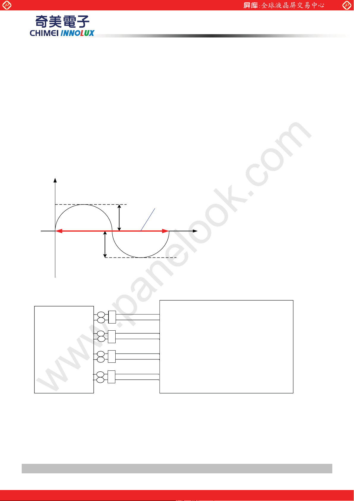
Note (1) Definition of Viewing Angle (θx, θy):
Viewing angles are measured by Autronic Conoscope Cono-80.
www.panelook.com
PRODUCT SPECIFICATION
Normal
θx = θy = 0º
θX- = 90º
x-
θy- θy+
θx−
θx+
12 o’clock direction
y+
θ
y+ = 90º
6 o’clock
θ
y- = 90º
y-
x+
θX+ = 90º
Note (2) Definition of Contrast Ratio (CR) :
The contrast ratio can be calculated by the following expression.
Contrast Ratio (CR) =
L255 of Luminance Surface
L0 of Luminance Surface
L255: Luminance of gray level 255
L 0: Luminance of gray level 0
CR = CR (5), where CR (X) is corresponding to the Contrast Ratio of the point X at the figure in Note (6).
Note (3) Definition of Gray to Gray Switching Time :
100%
90%
Optical
Response
10%
Gray to gray
switching time
The driving signal means the signal of gray level 0, 124, 252, 380, 508, 636, 764, 892 and 1023.
Gray to gray average time means the average switching time of gray level 0, 124, 252, 380, 508, 636,764,
892 and 1023 to each other.
Gray to gray
switching time
Version 2.0 27 DateΚΚ11 Jul 2011
The copyright belongs to CHIMEI InnoLux. Any unauthorized use is prohibited
One step solution for LCD / PDP / OLED panel application: Datasheet, inventory and accessory!
www.panelook.com
Page 28

Global LCD Panel Exchange Center
0%
T
ime
Note (4) Definition of Response Time (TR, TF):
www.panelook.com
PRODUCT SPECIFICATION
Gray Level 255
100%
90%
Optical
Response
10%
Note (5) Definition of Luminance of White (L
Measure the luminance of gray level 255 at center point and 5 points
L
= L (5), where L (X) is corresponding to the luminance of the point X at the figure in Note (6).
C
Gray Level 255
Gray Level 0
T
R
):
C
T
F
Version 2.0 28 DateΚΚ11 Jul 2011
The copyright belongs to CHIMEI InnoLux. Any unauthorized use is prohibited
One step solution for LCD / PDP / OLED panel application: Datasheet, inventory and accessory!
www.panelook.com
Page 29

Global LCD Panel Exchange Center
Active
(D, W)
Active
(0, 0)
(D, W)
Active
(D, W)
Active
(0, 0)
(D, W)
Note (6) Definition of Cross Talk (CT):
www.panelook.com
PRODUCT SPECIFICATION
CT = | Y
– YA | / YA × 100 (%)
B
Where:
YA = Luminance of measured location without gray level 0 pattern (cd/m2)
YB = Luminance of measured location with gray level 0 pattern (cd/m2)
(0, 0)
Y
(D/2,W/8)
A, U
Y
(D/8,W/2)
A, L
Gray 128
Y
A, D
Y
(7D/8,W/2)
A, R
(D/2,7W/8)
Y
B, L
(D/8,W/2)
YA = Luminance of measured location without gray level 255 pattern (cd/m2)
YB = Luminance of measured location with gray level 255 pattern (cd/m2)
(D/4,W/4)
Y
(D/2,W/8)
B, U
(3D/4,3W/4)
Y
(D/2,7W/8)
B, D
(7D/8,W/2)
Y
B, R
.
(0, 0)
Y
(D/2,W/8)
A, U
(D/4,W/4)
Y
B, U
(D/2,W/8)
Y
A, L
(D/8,W/2)
(D/2,7W/8)
Y
A, D
Y
(7D/8,W/2)
A, R
(D/8,W/2)
Y
B, L
Gray 128
(3D/4,3W/4)
(D/2,7W/8)
Y
B, D
(7D/8,W/2)
Y
B, R
Version 2.0 29 DateΚΚ11 Jul 2011
The copyright belongs to CHIMEI InnoLux. Any unauthorized use is prohibited
One step solution for LCD / PDP / OLED panel application: Datasheet, inventory and accessory!
www.panelook.com
Page 30

Global LCD Panel Exchange Center
W
G
Note (7) Definition of White Variation (δW):
Measure the luminance of gray level 255 at 5 points
δW = Maximum [L (1), L (2), L (3), L (4), L (5)] / Minimum [L (1), L (2), L (3), L (4), L (5)]
www.panelook.com
PRODUCT SPECIFICATION
Horizontal Line
Vertical Line
W/4
W/2
(D,
D/4 D/2 3D/4
1 2
3 4
D
5
Active Area
: Test Point
X=1 to 5
Version 2.0 30 DateΚΚ11 Jul 2011
The copyright belongs to CHIMEI InnoLux. Any unauthorized use is prohibited
One step solution for LCD / PDP / OLED panel application: Datasheet, inventory and accessory!
www.panelook.com
Page 31

Global LCD Panel Exchange Center
8. DEFINITION OF LABELS
8.1 CMO MODULE LABEL
The barcode nameplate is pasted on each module as illustration, and its definitions are as following explanation.
www.panelook.com
PRODUCT SPECIFICATION
V315B5-L10 Rev. XX
X X X X X X X Y M D L N N N N
V315B5-L10 Rev. XX
X X X X X X X Y M D L N N N N
MADE IN CHINA
LEOO(or CAPG or CANO)
RoHS
(a) Model Name: V315B5-L10
(b) Revision: Rev. XX, for example: A0, A1… B1, B2… or C1, C2…etc.
(c) Serial ID: X X
X X X X X Y M D L N N N N
Serial No.
Product Line
Year, Month, Date
CMO Internal Use
CMO Internal Use
Revision
CMO Internal Use
Version 2.0 31 DateΚΚ11 Jul 2011
The copyright belongs to CHIMEI InnoLux. Any unauthorized use is prohibited
One step solution for LCD / PDP / OLED panel application: Datasheet, inventory and accessory!
www.panelook.com
Page 32

Global LCD Panel Exchange Center
9. PACKAGING
9.1 PACKING SPECIFICATIONS
(1) 5 LCD TV modules / 1 Box
(2) Box dimensions : 826(L) X 376 (W) X 540 (H)
(3) Weight :
a.Panel module each pcs : 5.211 kg
b.Panel Packing Box
-Cushion : 0.494 kg ( 5 pcs per box)
-Carton : 2.3 kg
-Panel : 5.211 kg x 5pcs =26.055 kg
-Panel Packing Box Total (1 Box) =28.849 kg
c.Total Packing weight
www.panelook.com
PRODUCT SPECIFICATION
1) For Vessel shipment Pallet (1 Pallet =6 Box or 9 Box)
-Pallet weight : 12 kg
-Pallet Cushion : 2.96 kg or 4.44 kg
-Pallet Packing Total = 185.09 kg or 271.6 kg
2) For Air shipment Pallet (1 Pallet =6 Box)
-Pallet weight : 12 kg
-Pallet Cushion : 2.96 kg
-Pallet Packing Total =185.09 kg
9.2 PACKING METHOD
Figures 9-1 and 9-2 are the packing method
Figure.9-1 packing method
Version 2.0 32 DateΚΚ11 Jul 2011
The copyright belongs to CHIMEI InnoLux. Any unauthorized use is prohibited
One step solution for LCD / PDP / OLED panel application: Datasheet, inventory and accessory!
www.panelook.com
Page 33

Global LCD Panel Exchange Center
www.panelook.com
PRODUCT SPECIFICATION
Figure.9-2 packing method
Version 2.0 33 DateΚΚ11 Jul 2011
The copyright belongs to CHIMEI InnoLux. Any unauthorized use is prohibited
One step solution for LCD / PDP / OLED panel application: Datasheet, inventory and accessory!
www.panelook.com
Page 34

Global LCD Panel Exchange Center
www.panelook.com
PRODUCT SPECIFICATION
10. PRECAUTIONS
10.1 ASSEMBLY AND HANDLING PRECAUTIONS
(1) Do not apply rough force such as bending or twisting to the module during assembly.
(2) It is recommended to assemble or to install a module into the user’s system in clean working areas. The
dust and oil may cause electrical short or worsen the polarizer.
(3) Do not apply pressure or impulse to the module to prevent the damage of LCD panel and backlight.
(4) Always follow the correct power-on sequence when the LCD module is turned on. This can prevent the
damage and latch-up of the CMOS LSI chips.
(5) Do not plug in or pull out the I/F connector while the module is in operation.
(6) Do not disassemble the module.
(7) Use a soft dry cloth without chemicals for cleaning, because the surface of polarizer is very soft and
easily scratched.
(8) Moisture can easily penetrate into LCD module and may cause the damage during operation.
(9) High temperature or humidity may deteriorate the performance of LCD module. Please store LCD
modules in the specified storage conditions.
(10) When ambient temperature is lower than 10ºC, the display quality might be reduced. For example, the
response time will become slow, and the starting voltage of CCFL will be higher than that of room
temperature.
10.2 SAFETY PRECAUTIONS
(1) The startup voltage of a backlight is over 1000 Volts. It may cause an electrical shock while assembling
with the inverter. Do not disassemble the module or insert anything into the backlight unit.
(2) If the liquid crystal material leaks from the panel, it should be kept away from the eyes or mouth. In case
of contact with hands, skin or clothes, it has to be washed away thoroughly with soap.
(3) After the module’s end of life, it is not harmful in case of normal operation and storage.
Version 2.0 34 DateΚΚ11 Jul 2011
The copyright belongs to CHIMEI InnoLux. Any unauthorized use is prohibited
One step solution for LCD / PDP / OLED panel application: Datasheet, inventory and accessory!
www.panelook.com
Page 35

Global LCD Panel Exchange Center
11. MECHANICAL CHARACTERISTICS
www.panelook.com
PRODUCT SPECIFICATION
Version 2.0 35 DateΚΚ11 Jul 2011
The copyright belongs to CHIMEI InnoLux. Any unauthorized use is prohibited
One step solution for LCD / PDP / OLED panel application: Datasheet, inventory and accessory!
www.panelook.com
Page 36

Global LCD Panel Exchange Center
www.panelook.com
PRODUCT SPECIFICATION
Version 2.0 36 DateΚΚ11 Jul 2011
The copyright belongs to CHIMEI InnoLux. Any unauthorized use is prohibited
One step solution for LCD / PDP / OLED panel application: Datasheet, inventory and accessory!
www.panelook.com
Page 37

Global LCD Panel Exchange Center
www.panelook.com
PRODUCT SPECIFICATION
Version 2.0 37 DateΚΚ11 Jul 2011
The copyright belongs to CHIMEI InnoLux. Any unauthorized use is prohibited
One step solution for LCD / PDP / OLED panel application: Datasheet, inventory and accessory!
www.panelook.com
 Loading...