

Page 1
Global LCD Panel Exchange Center
MODEL NO.: V290BJ1
www.panelook.com
PRODUCT SPECIFICATION
ϭ Tentative Specification
ϭ Preliminary Specification
Ϯ Approval Specification
SUFFIX: LE1
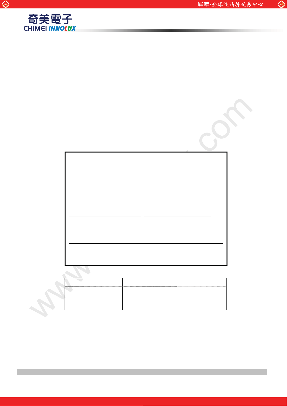
Customer:
APPROVED BY SIGNATURE
Name / Title
Note
Please return 1 copy for your confirmation with your signature and
comments.
Approved By Checked By Prepared By
Chao-Chun Chung
Version 2.0 1 DateΚΚ15 May 2012
The copyright belongs to CHIMEI InnoLux. Any unauthorized use is prohibited
One step solution for LCD / PDP / OLED panel application: Datasheet, inventory and accessory!
Vincent Chou Apple Wen
www.panelook.com
Page 2
Global LCD Panel Exchange Center
www.panelook.com
PRODUCT SPECIFICATION
CONTENTS
REVISION HISTORY....................................................................................................................................................................... 4
1. GENERAL DESCRIPTION ......................................................................................................................................................... 5
1.1 OVERVIEW......................................................................................................................................................................... 5
1.2 FEATURES .......................................................................................................................................................................... 5
1.3 APPLICATION................................................................................................................................................................... 5
1.4 GENERAL SPECIFICATIONS.......................................................................................................................................... 5
1.5 MECHANICAL SPECIFICATIONS................................................................................................................................. 7
2. ABSOLUTE MAXIMUM RATINGS .......................................................................................................................................... 8
2.1 ABSOLUTE RATINGS OF ENVIRONMENT................................................................................................................. 8
2.2 PACKAGE STORAGE ....................................................................................................................................................... 9
2.3 ELECTRICAL ABSOLUTE RATINGS............................................................................................................................. 9
2.3.1 TFT LCD MODULE....................................................................................................................................9
2.3.2 BACKLIGHT UNIT ....................................................................................................................................9
3. ELECTRICAL CHARACTERISTICS ....................................................................................................................................... 10
3.1 TFT LCD MODULE.......................................................................................................................................................... 10
3.2 BACKLIGHT UNIT.......................................................................................................................................................... 13
3.2.1 LED LIGHT BAR CHARACTERISTICS ...................................................................................................13
4. BLOCK DIAGRAM OF INTERFACE...................................................................................................................................... 14
4.1 TFT LCD MODULE.......................................................................................................................................................... 14
5. INPUT TERMINAL PIN ASSIGNMENT................................................................................................................................ 15
5.1 TFT LCD Module Input................................................................................................................................................... 15
5.2 LVDS INTERFACE........................................................................................................................................................... 17
5.3 COLOR DATA INPUT ASSIGNMENT......................................................................................................................... 18
6. INTERFACE TIMING................................................................................................................................................................ 19
6.1 INPUT SIGNAL TIMING SPECIFICATIONS.............................................................................................................. 19
6.2 POWER ON/OFF SEQUENCE ...................................................................................................................................... 22
7. OPTICAL CHARACTERISTICS............................................................................................................................................... 23
7.1 TEST CONDITIONS ........................................................................................................................................................ 23
7.2 OPTICAL SPECIFICATIONS ......................................................................................................................................... 24
Version 2.0 2 DateΚΚ15 May 2012
The copyright belongs to CHIMEI InnoLux. Any unauthorized use is prohibited
One step solution for LCD / PDP / OLED panel application: Datasheet, inventory and accessory!
www.panelook.com
Page 3

Global LCD Panel Exchange Center
www.panelook.com
PRODUCT SPECIFICATION
8. PRECAUTIONS.......................................................................................................................................................................... 27
8.1 ASSEMBLY AND HANDLING PRECAUTIONS........................................................................................................ 27
8.2 SAFETY PRECAUTIONS ................................................................................................................................................ 27
9. DEFINITION OF LABELS......................................................................................................................................................... 28
9.1 MODULE LABEL............................................................................................................................................................. 28
9.2 CARTON LABEL.............................................................................................................................................................. 29
10. PACKAGING............................................................................................................................................................................ 30
10.1 PACKAGING SPECIFICATIONS................................................................................................................................ 30
10.2 PACKAGING METHOD............................................................................................................................................... 30
11. MECHANICAL CHARACTERISTIC.................................................................................................................................... 32
Version 2.0 3 DateΚΚ15 May 2012
The copyright belongs to CHIMEI InnoLux. Any unauthorized use is prohibited
One step solution for LCD / PDP / OLED panel application: Datasheet, inventory and accessory!
www.panelook.com
Page 4
Global LCD Panel Exchange Center
www.panelook.com
REVISION HISTORY
Version Date Page(New) Section Description
Ver. 2.0
May.15, 2012 All
All
The approval specification was first issued.
PRODUCT SPECIFICATION
Version 2.0 4 DateΚΚ15 May 2012
The copyright belongs to CHIMEI InnoLux. Any unauthorized use is prohibited
One step solution for LCD / PDP / OLED panel application: Datasheet, inventory and accessory!
www.panelook.com
Page 5
Global LCD Panel Exchange Center
1. GENERAL DESCRIPTION
1.1 OVERVIEW
V290BJ1-LE1 is a 29” TFT Liquid Crystal Display module with LED Backlight unit and 1ch-LVDS interface. This
module supports 1366 x 768 HDTV format and can display 16.7M colors (8-bit).
1.2 FEATURES
Ё High brightness (300 nits)
Ё High contrast ratio (3000:1)
Ё Fast response time (Gray to gray average 9.5 ms)
Ё High color saturation (NTSC 72%)
Ё HDTV (1366 x 768 pixels) resolution
Ё DE (Data Enable) only mode
Ё LVDS (Low Voltage Differential Signaling) interface
Ё Optimized response time for 50/60 Hz frame rate
www.panelook.com
PRODUCT SPECIFICATION
Ё Ultra wide viewing angle : Super MVA technology
Ё RoHS compliance
1.3 APPLICATION
Ё Standard Living Room TVs.
Ё Public Display Application.
Ё Home Theater Application.
Ё MFM Application.
1.4 GENERAL SPECIFICATIONS
Item Specification Unit Note
Active Area 631.092 (H) x 354.816 (V) (29” diagonal) mm
Bezel Opening Area 635 (H) x 358.8 (V) mm
Driver Element a-si TFT active matrix - -
Pixel Number 1366 x R.G.B. x 768 pixel -
Pixel Pitch(Sub Pixel) 0.154 (H) x 0.462 (V) mm -
Pixel Arrangement RGB Vertical Stripe - -
(1)
Display Colors 16.7M color -
Display Operation Mode Transmissive mode / Normally black - -
Surface Treatment Anti-Glare coating (Haze 3.5%) - (2)
Rotation Function
Display Orientation
Note (1) Please refer to the attached drawings in chapter 9 for more information about the front and back outlines.
Note (2) The spec. of the surface treatment is temporarily for this phase. CMI reserves the rights to change this
Version 2.0 5 DateΚΚ15 May 2012
The copyright belongs to CHIMEI InnoLux. Any unauthorized use is prohibited
One step solution for LCD / PDP / OLED panel application: Datasheet, inventory and accessory!
Unachievable
Signal input with “CMI”
feature.
www.panelook.com
Page 6
Global LCD Panel Exchange Center
X+C Board
www.panelook.com
PRODUCT SPECIFICATION
Back Side
Front Side
CMI
Version 2.0 6 DateΚΚ15 May 2012
The copyright belongs to CHIMEI InnoLux. Any unauthorized use is prohibited
One step solution for LCD / PDP / OLED panel application: Datasheet, inventory and accessory!
www.panelook.com
Page 7
Global LCD Panel Exchange Center
1.5 MECHANICAL SPECIFICATIONS
Item Min. Typ. Max. Unit Note
Horizontal (H) 653.8 654.8 655.8 mm
www.panelook.com
PRODUCT SPECIFICATION
Module Size
Weight
Note (1) Please refer to the attached drawings for more information of front and back outline dimensions.
Note (2) Module Depth is between bezel to real.
Vertical (V) 379.7 380.7 381.7 mm
Depth (D) 18.3 19.3 20.3 mm
Ё
3.66 3.8 Kg
(1), (2)
Ё
Version 2.0 7 DateΚΚ15 May 2012
The copyright belongs to CHIMEI InnoLux. Any unauthorized use is prohibited
One step solution for LCD / PDP / OLED panel application: Datasheet, inventory and accessory!
www.panelook.com
Page 8
Global LCD Panel Exchange Center
www.panelook.com
2. ABSOLUTE MAXIMUM RATINGS
2.1 ABSOLUTE RATINGS OF ENVIRONMENT
Item Symbol
Storage Temperature TST -20 +60 ºC (1)
Operating Ambient Temperature TOP 0 50 ºC (1), (2)
Shock (Non-Operating) SNOP - 50 G (3), (5)
Vibration (Non-Operating) VNOP - 1.0 G (4), (5)
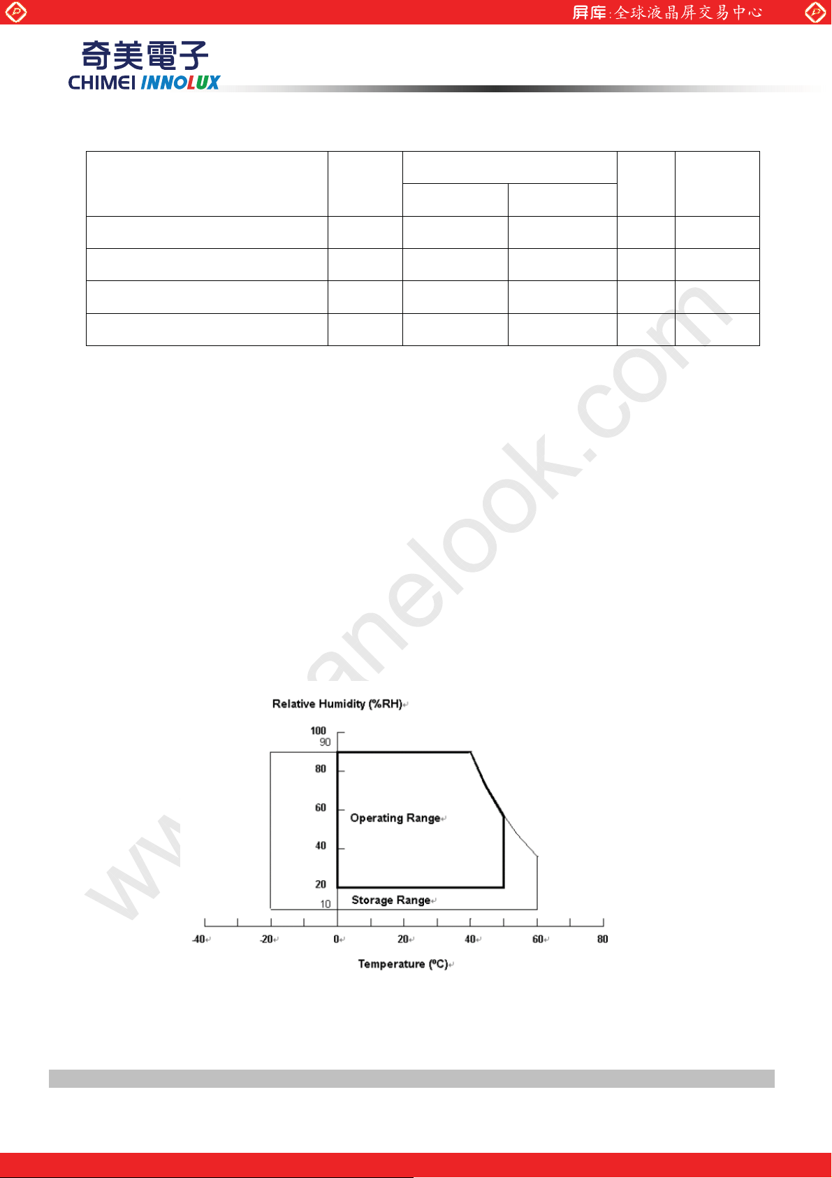
Note (1) Temperature and relative humidity range is shown in the figure below.
(a) 90 %RH Max. (Ta Љ 40 ºC).
(b) Wet-bulb temperature should be 39 ºC Max. (Ta > 40 ºC).
PRODUCT SPECIFICATION
Value
Unit Note
Min. Max.
(c) No condensation.
Note (2) The maximum operating temperature is based on the test condition that the surface temperature of
display area is less than or equal to 65 ºC with LCD module alone in a temperature controlled chamber.
Thermal management should be considered in final product design to prevent the surface temperature
of display area from being over 65 ºC. The range of operating temperature may degrade in case of
improper thermal management in final product design.
Note (3) 11 ms, half sine wave, 1 time for ± X, ± Y, ± Z.
Note (4) 10 ~ 200 Hz, 10 min, 1 time each X, Y, Z.
Note (5) At testing Vibration and Shock, the fixture in holding the module has to be hard and rigid enough so
that the module would not be twisted or bent by the fixture.
Version 2.0 8 DateΚΚ15 May 2012
The copyright belongs to CHIMEI InnoLux. Any unauthorized use is prohibited
One step solution for LCD / PDP / OLED panel application: Datasheet, inventory and accessory!
www.panelook.com
Page 9
Global LCD Panel Exchange Center
2.2 PACKAGE STORAGE
When storing modules as spares for a long time, the following precaution is necessary.
(a) Do not leave the module in high temperature, and high humidity for a long time, It is highly recommended
to store the module with temperature from 0 to 35 к at normal humidity without condensation.
(b) The module shall be stroed in dark place. Do not store the TFT-LCD module in direct sunlight or fluorescent
light.
2.3 ELECTRICAL ABSOLUTE RATINGS
2.3.1 TFT LCD MODULE
Item Symbol
Power Supply Voltage VCC -0.3 13.5 V
Logic Input Voltage VIN -0.3 3.6 V
www.panelook.com
PRODUCT SPECIFICATION
Value
Unit Note
Min. Max.
(1)
2.3.2 BACKLIGHT UNIT
Value
Item Symbol
Min. Max.
Light Bar Voltage VW
Note (1) Permanent damage to the device may occur if maximum values are exceeded. Function operation
should be restricted to the conditions described under Normal Operating Conditions
Ё
170 VDC (1)
Unit Note
Version 2.0 9 DateΚΚ15 May 2012
The copyright belongs to CHIMEI InnoLux. Any unauthorized use is prohibited
One step solution for LCD / PDP / OLED panel application: Datasheet, inventory and accessory!
www.panelook.com
Page 10
Global LCD Panel Exchange Center
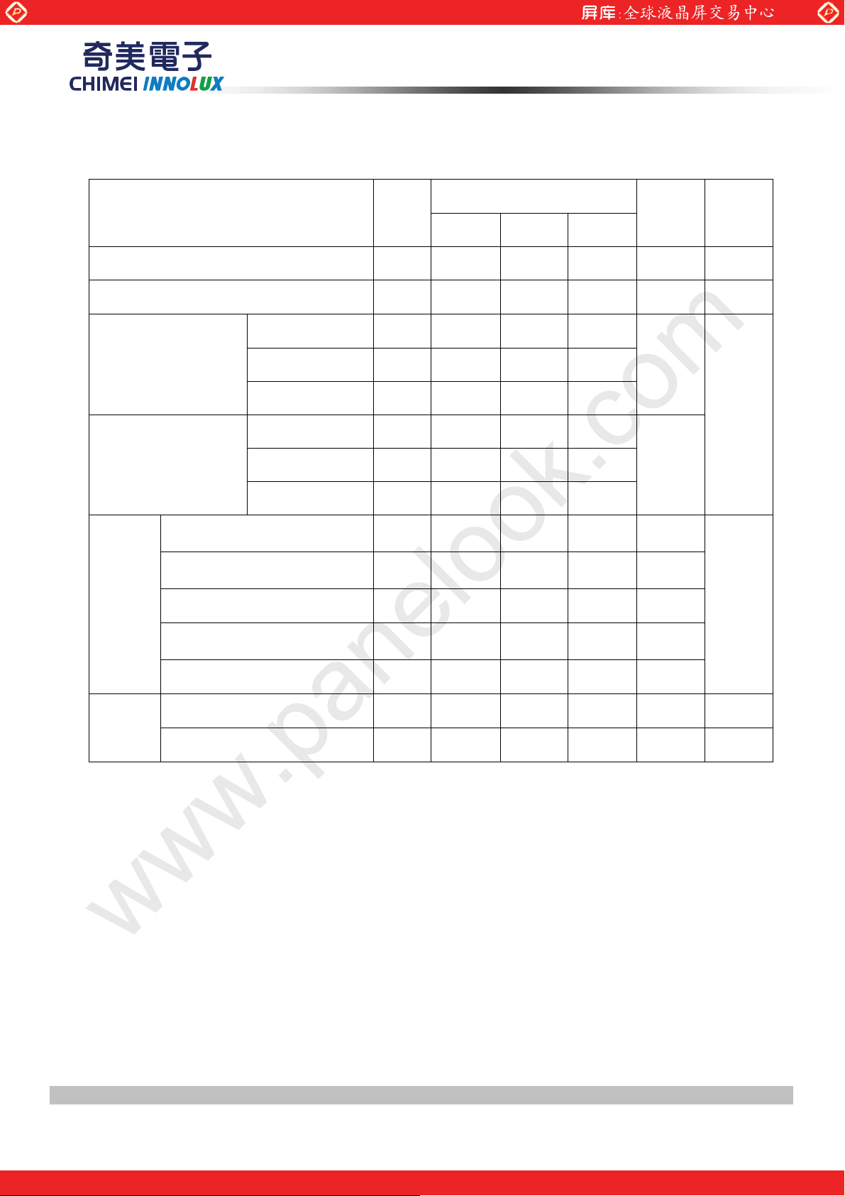
3. ELECTRICAL CHARACTERISTICS
3.1 TFT LCD MODULE
(Ta = 25 ± 2 ºC)
Parameter Symbol
Power Supply Voltage VCC 10.8 12 13.2 V (1)
www.panelook.com
PRODUCT SPECIFICATION
Value
Unit Note
Min. Typ. Max.
Rush Current I
White Pattern PT
Power consumption
Black Pattern PT
Horizontal Stripe P
White Pattern
Power Supply Current
Black Pattern
Horizontal Stripe
Differential Input High
Threshold Voltage
Differential Input Low
Threshold Voltage
LVDS
interface
Common Input Voltage VCM 1.0 1.2 1.4 V
Differential input voltage
(single-end)
Terminating Resistor R
RUSH
T
Ё Ё
Ё Ё
Ё Ё
V
LVTH
V
LVTL
|V
|
ID
T
Ё Ё
Ё
Ё
Ё
+100
-300
200
Ё
3.9 A (2)
5.04 6.72
3.12 4.32
5.28 6.96
0.42 0.56
0.26 0.36
0.44 0.58
Ё
Ё
Ё
100
+300 mV
-100 mV
600 mV
Ё
W
(3)
A
(4)
ohm
CMOS
interface
Input High Threshold Voltage VIH 2.7
Input Low Threshold Voltage V
0
IL
Ё
Ё
3.3 V
0.7 V
Note (1) The module should be always operated within the above ranges.
The ripple voltage should be controlled under 10% of Vcc (Typ.).
Note (2) Measurement condition :
Version 2.0 10 DateΚΚ15 May 2012
The copyright belongs to CHIMEI InnoLux. Any unauthorized use is prohibited
One step solution for LCD / PDP / OLED panel application: Datasheet, inventory and accessory!
www.panelook.com
Page 11

Global LCD Panel Exchange Center
www.panelook.com
PRODUCT SPECIFICATION
Note (3) The specified power supply current is under the conditions at Vcc = 12 V, Ta = 25 ± 2 ºC, f
whereas a power dissipation check pattern below is displayed.
GND
Vcc rising time is 470us
Vcc
0.9Vcc
0.1Vcc
470us
= 60 Hz,
v
Version 2.0 11 DateΚΚ15 May 2012
The copyright belongs to CHIMEI InnoLux. Any unauthorized use is prohibited
One step solution for LCD / PDP / OLED panel application: Datasheet, inventory and accessory!
www.panelook.com
Page 12

Global LCD Panel Exchange Center
a. White Pattern
www.panelook.com
PRODUCT SPECIFICATION
b. Black Pattern
Active Area
c. Horizontal Pattern
Note (4) The LVDS input characteristics are as follows:
Active Area
Version 2.0 12 DateΚΚ15 May 2012
The copyright belongs to CHIMEI InnoLux. Any unauthorized use is prohibited
One step solution for LCD / PDP / OLED panel application: Datasheet, inventory and accessory!
www.panelook.com
Page 13

Global LCD Panel Exchange Center
3.2 BACKLIGHT UNIT
3.2.1 LED LIGHT BAR CHARACTERISTICS
(Ta = 25 ± 2 ºC)
www.panelook.com
PRODUCT SPECIFICATION
Parameter Symbol
Min. Typ. Max.
Light Bar Current IL
Light Bar Voltage VW
Power Consumption PBL
Life time
Note (1) The lifetime is defined as the time which luminance of the LED decays to 50% compared to the
initial value, Operating condition: Continuous operating at Ta = 25±2к, I
Ё
150.4
144.48 161.4 178.32
27
30,000
Value
160 169.6
Ё Ё
L =160 mA
Unit Note
(1)
mA
V
DC
W
Hrs (1)
Duty=100%
IL =160mA
IL =160mA
Only LEDs
Duty=100%
I
=160mA
PIN
Version 2.0 13 DateΚΚ15 May 2012
The copyright belongs to CHIMEI InnoLux. Any unauthorized use is prohibited
One step solution for LCD / PDP / OLED panel application: Datasheet, inventory and accessory!
www.panelook.com
Page 14

Global LCD Panel Exchange Center
DATA DRIV
ER
SCAN DRIVER
DC/DC
CONVERTER
GND
SELLVDS
4. BLOCK DIAGRAM OF INTERFACE
4.1 TFT LCD MODULE
Vcc
RX0(+/-)
RX1(+/-)
RX2(+/-)
RX3(+/-)
CLK(+/-)
INPUT CONNECTOR, P-TWO 187099-30091
TIMING CONTROLLER
www.panelook.com
PRODUCT SPECIFICATION
TFT LCD PANEL
(1366x3x768)
CN1:CI0603S (3 Pin)
Pin 1 VLED+ (White Wire)
Pin 2 NC
Pin 3 VLED- (Black Wire)
& REFERENCE VOLTAGE
GENERATOR
BACKLIGHT UNIT
Version 2.0 14 DateΚΚ15 May 2012
The copyright belongs to CHIMEI InnoLux. Any unauthorized use is prohibited
One step solution for LCD / PDP / OLED panel application: Datasheet, inventory and accessory!
www.panelook.com
Page 15

Global LCD Panel Exchange Center
5. INPUT TERMINAL PIN ASSIGNMENT
5.1 TFT LCD Module Input
CNF1 Connector Pin Assignment (P-TWO 187099-30091)
Pin Name Description Note
1
2
3
4
5
6
7
8
9
10
11
12
13
14
15
16
17
18
19
20
21
22
23
24
25
26
27
28
29
30
VCC Power supply: +12V
VCC Power supply: +12V
VCC Power supply: +12V
VCC Power supply: +12V
GND Ground
GND Ground
GND Ground
NC No connection
SELLVDS
GND Ground
RX0- Negative transmission data of pixel 0
RX0+ Positive transmission data of pixel 0
GND Ground
RX1- Negative transmission data of pixel 1
RX1+ Positive transmission data of pixel 1
GND Ground
RX2- Negative transmission data of pixel 2
RX2+ Positive transmission data of pixel 2
GND Ground
RXCLK- Negative of clock
RXCLK+ Positive of clock
GND Ground
RX3- Negative transmission data of pixel 3
RX3+ Positive transmission data of pixel 3
GND Ground
GND Ground
LVDS data format Selection
NC No connection
NC No connection
NC No connection
NC No connection
www.panelook.com
PRODUCT SPECIFICATION
(2)
(3)(4)
(2)
(2)
(2)
(2)
Version 2.0 15 DateΚΚ15 May 2012
The copyright belongs to CHIMEI InnoLux. Any unauthorized use is prohibited
One step solution for LCD / PDP / OLED panel application: Datasheet, inventory and accessory!
www.panelook.com
Page 16

Global LCD Panel Exchange Center
TCON
Setting
LCM
S
ide System side
Note (1) Connector type: P-TWO 187099-30091
LVDS connector pin orderdefined as follows
Note (2) Reserved for internal use. Please leave it open.
Note (3) Connect to Open or +3.3V: VESA Format, connect to GND: JEIDA Format.
www.panelook.com
PRODUCT SPECIFICATION
SELLVDS Mode
H(default) VESA
L JEIDA
L: Connect to GND, H: Connect to +3.3V
Note (4)
Note (5) Two pixel data send into the module for every clock cycle. The first pixel of the frame is odd pixel and
LVDS signal pin connected to the LCM side has the following diagram. R1 in the system side should be
less than 1K Ohm. (R1 < 1K Ohm)
Selector (pin9)
the second pixel is even pixel.
R1
R2
Vcc
R3
Version 2.0 16 DateΚΚ15 May 2012
The copyright belongs to CHIMEI InnoLux. Any unauthorized use is prohibited
One step solution for LCD / PDP / OLED panel application: Datasheet, inventory and accessory!
www.panelook.com
Page 17

Global LCD Panel Exchange Center
5.2 LVDS INTERFACE
VESA LVDS formatΚ(SELLVDS pin=H/Open)
JEDIA LVDS formatΚ(SELLVDS pin=L)
www.panelook.com
PRODUCT SPECIFICATION
R0~R7 Pixel R Data (7; MSB,
0; LSB)
G0~G7 Pixel G Data (7; MSB,
0; LSB)
B0~B7 Pixel B Data (7; MSB,
0; LSB)
Note (1) RSVD (reserved) pins on the transmitter shall be “H” or “L”.
DE Data enable signal
DCLK Data clock signal
Version 2.0 17 DateΚΚ15 May 2012
The copyright belongs to CHIMEI InnoLux. Any unauthorized use is prohibited
One step solution for LCD / PDP / OLED panel application: Datasheet, inventory and accessory!
www.panelook.com
Page 18

Global LCD Panel Exchange Center
0 0
0 0
0 0
0 0
0 0
0 0
0 0
0 0
1 0
1 0
1 0
1 0
1 0
1 0
1 0
1 0
0 1
0 1
0 1
0 1
0 1
0 1
0 1
0 1
:
1 1
:
1 1
:
1 1
:
1 1
:
1 1
:
1 1
:
1 1
:
0 1
:
0 0
:
0 0
:
0 0
:
0 0
:
0 0
:
0 0
:
0 0
:
0 0
:
0 0
:
0 0
:
0 0
:
0 0
:
0 0
:
0 0
:
0 0
:
0 0
0
:
0
0
:
0
0
:
0
0
:
0
0
:
0
0
:
0
0
:
0
0
:
0
0
:
1
0
:
1
0
:
1
0
:
1
0
:
1
0
:
1
1
:
1
0
:
0
0
:
0
0
:
0
0
:
0
0
:
0
0
:
0
0
:
0
0
:
0
0
:
0
0
: 0 0 0
0
: 0 0 0
0
: 0 0 0
0
: 0 0 0
0
: 0 0 0
0
: 0 0 0
0
: 0 0 0
0
: 0 0 0
0
: 0 0 0
0
: 0 0 0
0
: 0 0 0
0
: 0 0 0
0
: 0 0 0
0
: 0 0 0
0
: 0 0 0
0
: 0 0 0
0
: 1 1 1
0
: 1 1 1
0
: 1 1 1
0
: 1 1 1
0
: 1 1 1
0
: 1 1 1
1
: 0 1 1
0
: 1 0 1
5.3 COLOR DATA INPUT ASSIGNMENT
The brightness of each primary color (red, green and blue) is based on the 8-bit gray scale data input for the color.
The higher the binary input, the brighter the color. The table below provides the assignment of the color versus
data input.
Color
R7 R6 R5 R4 R3 R2 R1 R0 G7 G6 G5 G4 G3 G2 G1 G0 B7 B6 B5 B4 B3 B2 B1 B0
Black
Red
Green
Basic
Colors
Gray
Scale
Of
Red
Gray
Scale
Of
Green
Gray
Scale
Of
Blue
Note (1) 0: Low Level Voltage, 1: High Level Voltage
Blue
Cyan
Magenta
Yellow
White
Red (0) / Dark
Red (1)
Red (2)
:
:
Red (253)
Red (254)
Red (255)
Green (0) / Dark
Green (1)
Green (2)
:
:
Green (253)
Green (254)
Green (255)
Blue (0) / Dark
Blue (1)
Blue (2)
:
:
Blue (253)
Blue (254)
Blue (255)
0
0
0
1
1
1
0
0
0
1
1
1
1
1
1
1
1
1
0
0
0
0
0
0
0
0
0
:
:
:
1
1
1
0
0
0
0
0
0
:
:
:
0
0
0
0
0
0
0
0
0
0
0
0
:
:
:
www.panelook.com
PRODUCT SPECIFICATION
Data Signal
Red Green Blue
0
0
0
0
0
0
0
0
0
0
0
0
0
0
0
0
0
0
0
0
0
1
1
1
1
1
0
0
0
0
0
0
0
0
0
0
0
0
0
0
0
0
0
0
0
0
0
1
1
1
1
1
1
1
1
1
1
1
1
1
1
1
1
1
1
1
1
1
0
0
0
0
0
0
0
0
1
1
1
1
1
1
1
1
1
1
1
1
1
1
1
1
1
1
1
1
1
0
0
0
0
0
0
0
0
1
1
1
1
1
1
1
1
1
1
1
1
1
1
1
1
1
1
1
1
1
0
0
0
0
0
0
0
0
0
0
0
0
0
0
0
0
0
0
0
0
0
0
0
0
0
1
0
0
0
0
0
0
0
0
0
0
0
0
0
0
0
0
0
0
0
1
0
0
0
0
0
0
0
0
0
0
0
0
0
0
0
0
0
:
:
:
:
:
:
:
:
:
:
:
:
:
:
:
:
:
:
:
:
:
1
1
1
0
1
0
0
0
0
0
0
0
0
0
0
0
0
0
0
0
0
0
0
0
0
0
0
0
0
0
0
0
0
0
0
0
0
0
0
0
0
0
0
0
0
0
0
0
0
0
0
0
0
0
1
0
0
0
0
0
0
0
0
:
:
:
:
:
:
:
:
:
:
:
:
:
:
:
:
:
:
:
:
:
0
0
0
0
0
1
1
1
1
1
1
0
1
0
0
0
0
0
0
0
0
0
0
0
0
0
1
1
1
1
1
1
1
1
0
0
0
0
0
0
0
0
0
0
0
0
0
0
0
0
0
0
0
0
0
0
0
0
0
0
0
0
0
0
0
0
0
0
0
0
0
0
0
0
0
0
0
0
0
0
0
0
0
1
:
:
:
:
:
:
:
:
:
:
:
:
:
:
:
:
:
:
:
:
:
Version 2.0 18 DateΚΚ15 May 2012
The copyright belongs to CHIMEI InnoLux. Any unauthorized use is prohibited
One step solution for LCD / PDP / OLED panel application: Datasheet, inventory and accessory!
www.panelook.com
Page 19

Global LCD Panel Exchange Center
6. INTERFACE TIMING
6.1 INPUT SIGNAL TIMING SPECIFICATIONS
(Ta = 25 ± 2 ºC)
The input signal timing specifications are shown as the following table and timing diagram.
www.panelook.com
PRODUCT SPECIFICATION
Signal Item Symbol
F
clkin
Frequency
(=1/TC
)
LVDS
Receiver
Clock
Input cycle to
cycle jitter
Spread spectrum
modulation range
T
clkin_mo
F
d
Spread spectrum
modulation
F
SSM
frequency
LVDS
Receiver
Data
Receiver Skew
Margin
T
RSKM
Fr5 47 50 53 Hz
Frame Rate
Vertical
Active
Display
Term
Total Tv 778 806 986 Th
Display Tvd 768 768 768 Th
F
Blank Tvb 10 38 218 Th
Min. Typ. Max. Unit Note
60 76 82 MHz
rcl
Ё Ё
-2%
F
clkin
Ё
200 ps (3)
F
clkin
+2%
MHz
57 60 63 Hz
r6
Ё Ё
-400
Ё
200 KHz
400 ps (5)
(4)
(6)
Tv=Tvd+Tvb
Ё
Ё
Horizontal
Active
Display
Term
Total Th 1446 1560 1936 Tc
Display Thd 1366 1366 1366 Tc
Blank Thb 80 194 570 Tc
Th=Thd+Thb
Ё
Ё
Note (1) Please make sure the range of pixel clock has follow the below equationΚ
F
clkin(max) Њ Fr6 Ѽ Tv Ѽ Th
Fr5 Ѽ Tv Ѽ Th Њ Fclkin(min)
Note (2) This module is operated in DE only mode and please follow the input signal timing diagram belowΚ
Version 2.0 19 DateΚΚ15 May 2012
The copyright belongs to CHIMEI InnoLux. Any unauthorized use is prohibited
One step solution for LCD / PDP / OLED panel application: Datasheet, inventory and accessory!
www.panelook.com
Page 20

Global LCD Panel Exchange Center
Thb
Tc
DE
Th
www.panelook.com
PRODUCT SPECIFICATION
Tv
Tvd
Tvb
Note (3) The input clock cycle-to-cycle jitter is defined as below figures. Trcl = | T
DCLK
DE
DATA
Thd
Valid Display Data (1366 clocks)
– T|
1
Version 2.0 20 DateΚΚ15 May 2012
The copyright belongs to CHIMEI InnoLux. Any unauthorized use is prohibited
One step solution for LCD / PDP / OLED panel application: Datasheet, inventory and accessory!
www.panelook.com
Page 21

Global LCD Panel Exchange Center
www.panelook.com
PRODUCT SPECIFICATION
Note (4) The SSCG (Spread spectrum clock generator) is defined as below figures.
Note (5) The LVDS timing diagram and setup/hold time is defined and showing as the following figure.
LVDS RECEIVER INTERFACE TIMING DIAGRAM
RXCLK+/-
RXn+/-
T
RSKM
Version 2.0 21 DateΚΚ15 May 2012
The copyright belongs to CHIMEI InnoLux. Any unauthorized use is prohibited
One step solution for LCD / PDP / OLED panel application: Datasheet, inventory and accessory!
www.panelook.com
Page 22

Global LCD Panel Exchange Center
100ms
ЉT6
6.2 POWER ON/OFF SEQUENCE
(Ta = 25 ± 2 ºC)
To prevent a latch-up or DC operation of LCD module, the power on/off sequence should be as the diagram
below.
www.panelook.com
0.9Vcc
PRODUCT SPECIFICATION
0.9Vcc
0.5ɩT1ɩ10ms
0ɩT2ɩ200ms
0ɩT3
500ms ɩT4
0V
0.1V
CC
3 T1
T
2
T
0.1V
T4
cc
LVDS Signals
0V
Power On
Power Off
0ЉT7ЉT2
0ЉT8ЉT3
T7
T
8
Option Signals
(SELLVDS)
Backlight (Recommended)
500msЉT5
50%
50%
T
5
6
T
Power ON/OFF Sequence
Note (1) The supply voltage of the external system for the module input should follow the definition of Vcc.
Note (2) Apply the lamp voltage within the LCD operation range. When the backlight turns on before the LCD
operation or the LCD turns off before the backlight turns off, the display may momentarily become
abnormal screen.
Note (3) In case of Vcc is in off level, please keep the level of input signals on the low or high impedance.
Note (4) T4 should be measured after the module has been fully discharged between power off and on period.
Note (5) Interface signal shall not be kept at high impedance when the power is on.
Version 2.0 22 DateΚΚ15 May 2012
The copyright belongs to CHIMEI InnoLux. Any unauthorized use is prohibited
One step solution for LCD / PDP / OLED panel application: Datasheet, inventory and accessory!
www.panelook.com
Page 23

Global LCD Panel Exchange Center
500
LCD
LCD
Light Shield Room
l
7. OPTICAL CHARACTERISTICS
7.1 TEST CONDITIONS
Item Symbol Value Unit
www.panelook.com
PRODUCT SPECIFICATION
Ambient Temperature Ta
Ambient Humidity Ha
Supply Voltage VCC 12 V
Input Signal According to typical value in "3. ELECTRICAL CHARACTERISTICS"
LED Current IL 160 mA
Vertical Frame Rate Fr 60 Hz
Note : No guarantee level of water flow
The LCD module should be stabilized at given temperature for 1 hour to avoid abrupt temperature change
during measuring. In order to stabilize the luminance, the measurement should be executed after lighting
backlight for 1 hour in a windless room.
M odule
anel
P
CS -2000
25±2
50±10
oC
%RH
Field of View = 1º
mm
Ambient uminance < 2 x)
(
L
u
Version 2.0 23 DateΚΚ15 May 2012
The copyright belongs to CHIMEI InnoLux. Any unauthorized use is prohibited
One step solution for LCD / PDP / OLED panel application: Datasheet, inventory and accessory!
www.panelook.com
Page 24

Global LCD Panel Exchange Center
7.2 OPTICAL SPECIFICATIONS
The relative measurement methods of optical characteristics are shown in 7.2. The following items should be
measured under the test conditions described in 7.1 and stable environment shown in 7.1.
www.panelook.com
PRODUCT SPECIFICATION
Item Symbol
Contrast Ratio CR 2100 3000
Response Time
Center Luminance of White LC 240 300
White Variation
Cross Talk CT 4 % Note (5)
Red
Green
Color
Chromaticity
Blue
White
Gray to
gray
δW
Rx 0.634
Ry 0.338
Gx 0.312
Gy 0.623
Bx 0.149
By 0.058
Wx 0.280
Wy
Condition Min. Typ. Max. Unit Note
- Note (2)
9.5 18 ms
cd/m
2
1.4 - Note (6)
-
θx=0°, θy =0°
Viewing angle
at normal direction
Typ.
-0.03
Typ.
+0.03
0.290
-
-
-
-
-
-
-
Note (3)
Note (4)
Color Gamut
Horizontal
Viewing
Angle
Vertical
Note (1) Definition of Viewing Angle (θx, θy) :
Viewing angles are measured by Conoscope Cono-80 (or Eldim EZ-Contrast 160R )
C.G
θx+
θx-
θY+
θY-
CR≥20
72 - % NTSC
80 88 -
80 88 -
Deg.
80 88 -
80 88 -
Note (1)
Version 2.0 24 DateΚΚ15 May 2012
The copyright belongs to CHIMEI InnoLux. Any unauthorized use is prohibited
One step solution for LCD / PDP / OLED panel application: Datasheet, inventory and accessory!
www.panelook.com
Page 25

Global LCD Panel Exchange Center
www.panelook.com
PRODUCT SPECIFICATION
Normal
θX- = 90º
6 o’clock
θ
y- = 90º
Note (2) Definition of Contrast Ratio (CR) :
The contrast ratio can be calculated by the following expression.
Contrast Ratio (CR) =
L255: Luminance of gray level 255
x-
y-
θx = θy = 0º
θy- θy+
θx−
θx+
y+
L255 of Luminance Surface
L0 of Luminance Surface
12 o’clock direction
θ
y+ = 90º
x+
θX+ = 90º
L0: Luminance of gray level 0
CR = CR (5), where CR (X) is corresponding to the Contrast Ratio of the point X at the figure in Note (6).
Note (3) Definition of Gray-to-Gray Switching Time:
The driving signal means the signal of gray level 0, 31, 63, 95, 127, 159, 191, 223 and 255. Gray to gray
average time means the average switching time of gray level 0, 31, 63, 95, 127, 159, 191, 223 and 255 to
each other.
Version 2.0 25 DateΚΚ15 May 2012
The copyright belongs to CHIMEI InnoLux. Any unauthorized use is prohibited
One step solution for LCD / PDP / OLED panel application: Datasheet, inventory and accessory!
www.panelook.com
Page 26

Global LCD Panel Exchange Center
Active Area
(D, W
)
Active Area
(0, 0)
Note (4) Definition of Luminance of White (LC, L
Measure the luminance of gray level 255 at center point and 5 points
L
= L (5), where L (X) is corresponding to the luminance of the point X at the figure in Note (6).
C
Note (5) Definition of Cross Talk (CT) :
CT = | YB – YA | / YA × 100 (%)
Where :
YA = Luminance of measured location without gray level 255 pattern (cd/m2)
YB = Luminance of measured location with gray level 255 pattern (cd/m2)
(0, 0)
Y
(D/2,W/8)
A,U
www.panelook.com
PRODUCT SPECIFICATION
) :
AVE
Y
(D/4,W/4)
(D/2,W/8)
B, U
(D/8,W/2)
Y
A,L
Gray 128
Y
(7D/8,W/2)
A, R
Y
(D/2,7W/8)
A, D
Note (6) Definition of White Variation (δW) :
Measure the luminance of gray level 255 at 5 points
δW = Maximum [L (1), L (2), L (3), L (4), L (5)] / Minimum [L (1), L (2), L (3), L (4), L (5)]
Y
(D/8,W/2)
B, L
Gray 255
Y
(D/2,7W/8)
B, D
(7D/8,W/2)
Y
A, R
(3D/4,3W/4)
Version 2.0 26 DateΚΚ15 May 2012
The copyright belongs to CHIMEI InnoLux. Any unauthorized use is prohibited
One step solution for LCD / PDP / OLED panel application: Datasheet, inventory and accessory!
www.panelook.com
Page 27

Global LCD Panel Exchange Center
www.panelook.com
PRODUCT SPECIFICATION
8. PRECAUTIONS
8.1 ASSEMBLY AND HANDLING PRECAUTIONS
[ 1 ] Do not apply rough force such as bending or twisting to the module during assembly.
[ 2 ] It is recommended to assemble or to install a module into the user’s system in clean working areas. The dust
and oil may cause electrical short or worsen the polarizer.
[ 3 ] Do not apply pressure or impulse to the module to prevent the damage of LCD panel and Backlight.
[ 4 ] Always follow the correct power-on sequence when the LCD module is turned on. This can prevent the
damage and latch-up of the CMOS LSI chips.
[ 5 ] Do not plug in or pull out the I/F connector while the module is in operation.
[ 6 ] Do not disassemble the module.
[ 7 ] Use a soft dry cloth without chemicals for cleaning, because the surface of polarizer is very soft and easily
scratched.
[ 8 ] Moisture can easily penetrate into LCD module and may cause the damage during operation.
[ 9 ] When storing modules as spares for a long time, the following precaution is necessary.
[ 9.1 ] Do not leave the module in high temperature, and high humidity for a long time. It is highly
recommended to store the module with temperature from 0 to 35кat normal humidity without
condensation.
[ 9.2 ] The module shall be stored in dark place. Do not store the TFT-LCD module in direct sunlight or
fluorescent light.
[ 10 ] When ambient temperature is lower than 10ºC, the display quality might be reduced. For example, the
response time will become slow, and the starting voltage of CCFL will be higher than that of room
temperature.
8.2 SAFETY PRECAUTIONS
[ 1 ] The startup voltage of a Backlight is approximately 1000 Volts. It may cause an electrical shock while
assembling with the inverter. Do not disassemble the module or insert anything into the Backlight unit.
[ 2 ] If the liquid crystal material leaks from the panel, it should be kept away from the eyes or mouth. In case of
contact with hands, skin or clothes, it has to be washed away thoroughly with soap.
[ 3 ] After the module’s end of life, it is not harmful in case of normal operation and storage.
Version 2.0 27 DateΚΚ15 May 2012
The copyright belongs to CHIMEI InnoLux. Any unauthorized use is prohibited
One step solution for LCD / PDP / OLED panel application: Datasheet, inventory and accessory!
www.panelook.com
Page 28

Global LCD Panel Exchange Center
9. DEFINITION OF LABELS
9.1 MODULE LABEL
The barcode nameplate is pasted on each module as illustration, and its definitions are as following explanation.
www.panelook.com
PRODUCT SPECIFICATION
Model Name: V290BJ1-LE1
Revision: Rev. XX, for example: A0, A1… B1, B2… or C1, C2…etc.
Serial ID: X X X X X X X Y M D L N N N N
Serial ID includes the information as below :
CHI MEI
OPTOELECTRONICS
V290BJ1-LE1 Rev. XX
X X X X X X X Y M D L N N N N
Serial No.
Product Line
Year, Month, Date
CMI Internal Use
CMI Internal Use
Revision
CMI Internal Use
MADE IN CHINA
LEOO(or CAPG or CANO)
RoHS
Manufactured Date:
Year : 2010=0, 2011=1, 2012=2…etc.
Month : 1~9, A~C, for Jan. ~ Dec.
Day : 1~9, A~Y, for 1st to 31st, exclude I ,O, and U.
Revision Code: Cover all the change
Serial No.: Manufacturing sequence of product
Product Line: 1 Ш Line1, 2 Ш Line 2, …etc.
Version 2.0 28 DateΚΚ15 May 2012
The copyright belongs to CHIMEI InnoLux. Any unauthorized use is prohibited
One step solution for LCD / PDP / OLED panel application: Datasheet, inventory and accessory!
www.panelook.com
Page 29

Global LCD Panel Exchange Center
9.2 CARTON LABEL
The barcode nameplate is pasted on each box as illustration, and its definitions are as following explanation.
www.panelook.com
PRODUCT SPECIFICATION
(a) Model Name: V290BJ1– LE1
(b) Carton ID: X X X X X X X Y M D X X X X
P.O. NO.
Parts ID.
Model Name V290BJ1-LE1
Carton ID. Quantities
XXXXXXXXXXXXXX
Made In Taiwan (Made In China)
CMI Internal Use
Serial ID includes the information as below :
Manufactured Date:
Year: 2010=0, 2011=1, 2012=2…etc.
Month: 1~9, A~C, for Jan. ~ Dec.
Day: 1~9, A~Y, for 1st to 31st, exclude I ,O, and U.
Revision Code: Cover all the change
Year, Month, Date
CMI Internal Use
Revision
CMI Internal Use
Version 2.0 29 DateΚΚ15 May 2012
The copyright belongs to CHIMEI InnoLux. Any unauthorized use is prohibited
One step solution for LCD / PDP / OLED panel application: Datasheet, inventory and accessory!
www.panelook.com
Page 30

Global LCD Panel Exchange Center
10. PACKAGING
10.1 PACKAGING SPECIFICATIONS
(1) 8 LCD TV modules / 1 Box
(2) Box dimensions : 713(L)x429(W)x453(H)mm
(3) Weight : Approx. 32.6 Kg (modules per carton)
10.2 PACKAGING METHOD
Packing methods are shown in following figures.
www.panelook.com
PRODUCT SPECIFICATION
Panel Protect Film
Tape
LCD TV Module
Cushion(Bottom)
Note:T-CON
Downward
Carton
LCD TV Module
Anti-Static Bag
LCD TV Module
Note:T-CON
Downward
Carton Label
Version 2.0 30 DateΚΚ15 May 2012
The copyright belongs to CHIMEI InnoLux. Any unauthorized use is prohibited
One step solution for LCD / PDP / OLED panel application: Datasheet, inventory and accessory!
www.panelook.com
Page 31

Global LCD Panel Exchange Center
www.panelook.com
PRODUCT SPECIFICATION
Version 2.0 31 DateΚΚ15 May 2012
The copyright belongs to CHIMEI InnoLux. Any unauthorized use is prohibited
One step solution for LCD / PDP / OLED panel application: Datasheet, inventory and accessory!
www.panelook.com
Page 32

Global LCD Panel Exchange Center
11. MECHANICAL CHARACTERISTIC
www.panelook.com
PRODUCT SPECIFICATION
Version 2.0 32 DateΚΚ15 May 2012
The copyright belongs to CHIMEI InnoLux. Any unauthorized use is prohibited
One step solution for LCD / PDP / OLED panel application: Datasheet, inventory and accessory!
www.panelook.com
Page 33

Global LCD Panel Exchange Center
www.panelook.com
PRODUCT SPECIFICATION
Version 2.0 33 DateΚΚ15 May 2012
The copyright belongs to CHIMEI InnoLux. Any unauthorized use is prohibited
One step solution for LCD / PDP / OLED panel application: Datasheet, inventory and accessory!
www.panelook.com
 Loading...