

Page 1
Global LCD Panel Exchange Center
ுழၴ ຝ ᐉு ߡۥ ދป
ขጥ
吳
柏 勳
TFT LCD Approval Specification
MODEL NO.: V236H2- L01
www.panelook.com
Issued Date: May. 11, 2010
Model No.: V236H2 - L01
Approval
Customer: _______________________________
Approved by:_______________________________
Note:
2010-05-20
16:34:35
MTR
2010.05.20
Director Accept
1
One step solution for LCD / PDP / OLED panel application: Datasheet, inventory and accessory!
Version 2.0
www.panelook.com
Page 2
Global LCD Panel Exchange Center
www.panelook.com
Issued Date: May. 11, 2010
Model No.: V236H2 - L01
Approval
CONTENTS
REVISION HISTORY ------------------------------------------------------- 3
1. GENERAL DESCRIPTION
1.1 OVERVIEW
1.2 FEATURES
1.3 GENERAL
1.4 MECHANICAL
------------------------------------------------------- 4
2. ABSOLUTE MAXIMUM RATINGS ------------------------------------------------------- 5
2.1 ABSOLUTE RATINGS OF ENVIRONMENT
2.2 TFT LCD MODULE
2.3 BACKLIGHT UNIT
3. ELECTRICAL CHARACTERISTICS ------------------------------------------------------- 7
3.1 TFT LCD MODULE
3.1.1 Vcc POWER DIP CONDITION
3.2 CCFL (Cold Cathode Fluorescent Lamp) CHARACTERISTICS
4. BLOCK DIAGRAM ------------------------------------------------------- 11
4.1 TFT LCD MODULE
4.2 BACKLIGHT UNIT
5. INPUT TERMINAL PIN ASSIGNMENT ------------------------------------------------------- 12
5.1 TFT LCD MODULE
5.2 LVDS DATA MAPPING TABLE
5.3 BACKLIGHT UNIT
5.4 COLOR DATA INPUT ASSIGNMENT
6. INTERFACE TIMING ------------------------------------------------------- 15
6.1 INPUT SIGNAL TIMING SPECIFICATIONS
6.2 POWER ON/OFF SEQUENCE
7. OPTICAL CHARACTERISTICS ------------------------------------------------------- 19
7.1 TEST CONDITIONS
7.2 OPTICAL SPECIFICATIONS
8. DEFINITION OF LABELS ------------------------------------------------------- 23
8.1 CMO MODULE LABEL
9. PACKAGING ------------------------------------------------------- 24
9.1 PACKING SPECIFICATIONS
9.2 PACKING METHOD
10. PRECAUTIONS ------------------------------------------------------- 26
10.1 ASSEMBLY AND HANDLING PRECAUTIONS
10.2 SAFETY PRECAUTIONS
10.3 SAFETY STANDARDS
11. MECHANICAL CHARACTERISTICS ------------------------------------------------------- 27
2
One step solution for LCD / PDP / OLED panel application: Datasheet, inventory and accessory!
Version 2.0
www.panelook.com
Page 3
Global LCD Panel Exchange Center
www.panelook.com
Issued Date: May. 11, 2010
Model No.: V236H2 - L01
Approval
REVISION HISTORY
Version Date
Ver 2.0
May. 11,’10
Page
(New)
All
Section Description
All
Approval Specification was first issued.
3
One step solution for LCD / PDP / OLED panel application: Datasheet, inventory and accessory!
Version 2.0
www.panelook.com
Page 4
Global LCD Panel Exchange Center
1.GENERAL DESCRIPTION
1.1 OVERVIEW
The V236H2-L01 model is a 23.6 inch wide TFT-LCD module with a 2 U-type CCFL Backlight Unit and a 30-pin
2ch-LVDS interface. This module supports 1920 x 1080 (16:9 wide screen) mode and displays up to 16.7
( 6-bit+Hi-FRC colors) millions colors. The inverter module for the Backlight Unit is not built in.
1.2 FEATURES
- Excellent Brightness: 300nits
- Contrast Ratio: 800:1
- Fast Response Time: 5ms
- Color Saturation: NTSC 72%
- Full HD (1920 x 1080 pixels) Resolution
- DE (Data Enable) Only Mode
www.panelook.com
Issued Date: May. 11, 2010
Model No.: V236H2 - L01
Approval
- mini-LVDS (Low Voltage Differential Signaling) Interface
- Viewing Angle: 170(H)/160(V) (CR>10) TN Technology
- Gate On Panel Technology
1.3 GENERAL
Item Specification Unit Note
Active Area 521.28(H) x 293.22(V) (23.547” real diagonal) mm
Bezel Opening Area 525.22 (H) x 297.22 (V) mm
Driver Element a-Si TFT active matrix -
Pixel Number 1920 x R.G.B. x 1080 pixel
Pixel Pitch 0.2715 (H) x 0.2715 (V) mm
Pixel Arrangement RGB vertical stripe -
Display Colors 16.7M color
Transmissive Mode Normally White -
Surface Treatment AG type, 3H hard coating, Haze 25 -
1.4 MECHANICAL
Item Min. Typ. Max. Unit Note
Horizontal(H) 543.8 544.8 545.8 mm
Module Size
Vertical(V) 319.5 320.5 321.5 mm
Depth(D) 45.7 46.7 47.7 mm To Rear
Depth(D) 50.7 51.7 52.7 mm To Boss
Weight - 2400 - g -
(1)
4
One step solution for LCD / PDP / OLED panel application: Datasheet, inventory and accessory!
Version 2.0
www.panelook.com
Page 5
Global LCD Panel Exchange Center
к
2. ABSOLUTE MAXIMUM RATINGS
2.1 ABSOLUTE RATINGS OF ENVIRONMENT
www.panelook.com
Issued Date: May. 11, 2010
Model No.: V236H2 - L01
Approval
Item Symbol
Storage Temperature TST
Operating Ambient Temperature TOP
Shock (Non-Operating) SNOP
Vibration (Non-Operating) VNOP
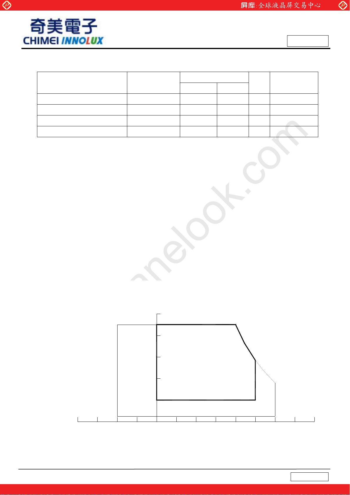
Note (1) Temperature and relative humidity range is shown in the figure below.
(a) 90% RH Max. (Ta 40 Љк).
(b) Wet-bulb temperature should be 39 к Max. (Ta > 40 к).
(c) No condensation.
Note (2) The maximum operating temperature is based on the test condition that the surface temperature of
display area is less than or equal to 65 к with LCD module alone in a temperature controlled chamber.
Thermal management should be considered in final product design to prevent the surface temperature
of display area from being over 65 к. The range of operating temperature may degrade in case of
improper thermal management in final product design.
Note (3) 11 ms, half-sine wave, 1 time for ± X, ± Y, ± Z.
Value
Min. Max.
-20 +60
0 +50
- 50 G (3), (5)
- 1.0 G (4), (5)
Unit Note
к
к
(1)
(1), (2)
Note (4) 10 ~ 200 Hz, 10 min, 1 time each X, Y, Z.
Note (5) At testing Vibration and Shock, the fixture in holding the module has to be hard and rigid enough so that
the module would not be twisted or bent by the fixture.
Relative Humidity (%RH)
100
90
80
60
Operating Range
40
20
10
Storage Range
Temperature (
5
)
One step solution for LCD / PDP / OLED panel application: Datasheet, inventory and accessory!
8060-20 40 0 20 -40
Version 2.0
www.panelook.com
Page 6
Global LCD Panel Exchange Center
2.2 TFT LCD MODULE
Item Symbol
Power Supply Voltage Vcc -0.3 6.0 V
Input Signal Voltage VIN -0.3 3.6 V
2.3 BACKLIGHT UNIT
Item Symbol
www.panelook.com
Value
Min. Max.
Value
Min. Typ. Max.
Issued Date: May. 11, 2010
Model No.: V236H2 - L01
Approval
Unit Note
Unit Note
Lamp Voltage VL 972 1080 1188 V
Lamp Current IL 12.0 12.5 13.0 mA
Lamp Frequency FL 30 -- 80
Note (1) Permanent damage to the device may occur if maximum values are exceeded. Functional operation
should be restricted to the conditions described under normal operating conditions.
Note (2) No moisture condensation or freezing.
(1), (2)
RMS
RMS
(1), (2)
6
One step solution for LCD / PDP / OLED panel application: Datasheet, inventory and accessory!
Version 2.0
www.panelook.com
Page 7
Global LCD Panel Exchange Center
www.panelook.com
Issued Date: May. 11, 2010
Model No.: V236H2 - L01
3. ELECTRICAL CHARACTERISTICS
3.1 TFT LCD MODULE Ta = 25 ± 2 ºC
Parameter Symbol
Power Supply Voltage Vcc 4.5 5.0 5.5 V -
Ripple Voltage VRP -- -- 300 mV -
Power on Rush Current I
White -- 0.69 0.97 A (3)a
Power Supply Current
Power Consumption PLCD -- 5.45 7.63 Watt (4)
LVDS differential input voltage Vid 200 -- 600 mV (5)
LVDS common input voltage Vic 1.0 1.2 1.4 V
Logic High Input Voltage VIH 2.64 -- -- V
Logic Low Input Voltage VIL 0 -- 0.66 V
Black -- 1.09 1.53 A (3)b
Vertical Stripe
RUSH
Min. Typ. Max.
-- -- 3.5 A (2)
-- 0.98 1.37 A (3)c
Value
Unit Note
Approval
Note (1) The module should be always operated within above ranges.
Note (2) Power on rush current measurement conditions:
Vcc rising time is 470us
Vcc
0.9Vcc
0.1Vcc
GND
470us
Note (3) The specified power supply current is under the conditions at Vcc = 5 V, Ta = 25 ± 2 к, f
7
One step solution for LCD / PDP / OLED panel application: Datasheet, inventory and accessory!
= 60 Hz,
v
Version 2.0
www.panelook.com
Page 8
Global LCD Panel Exchange Center
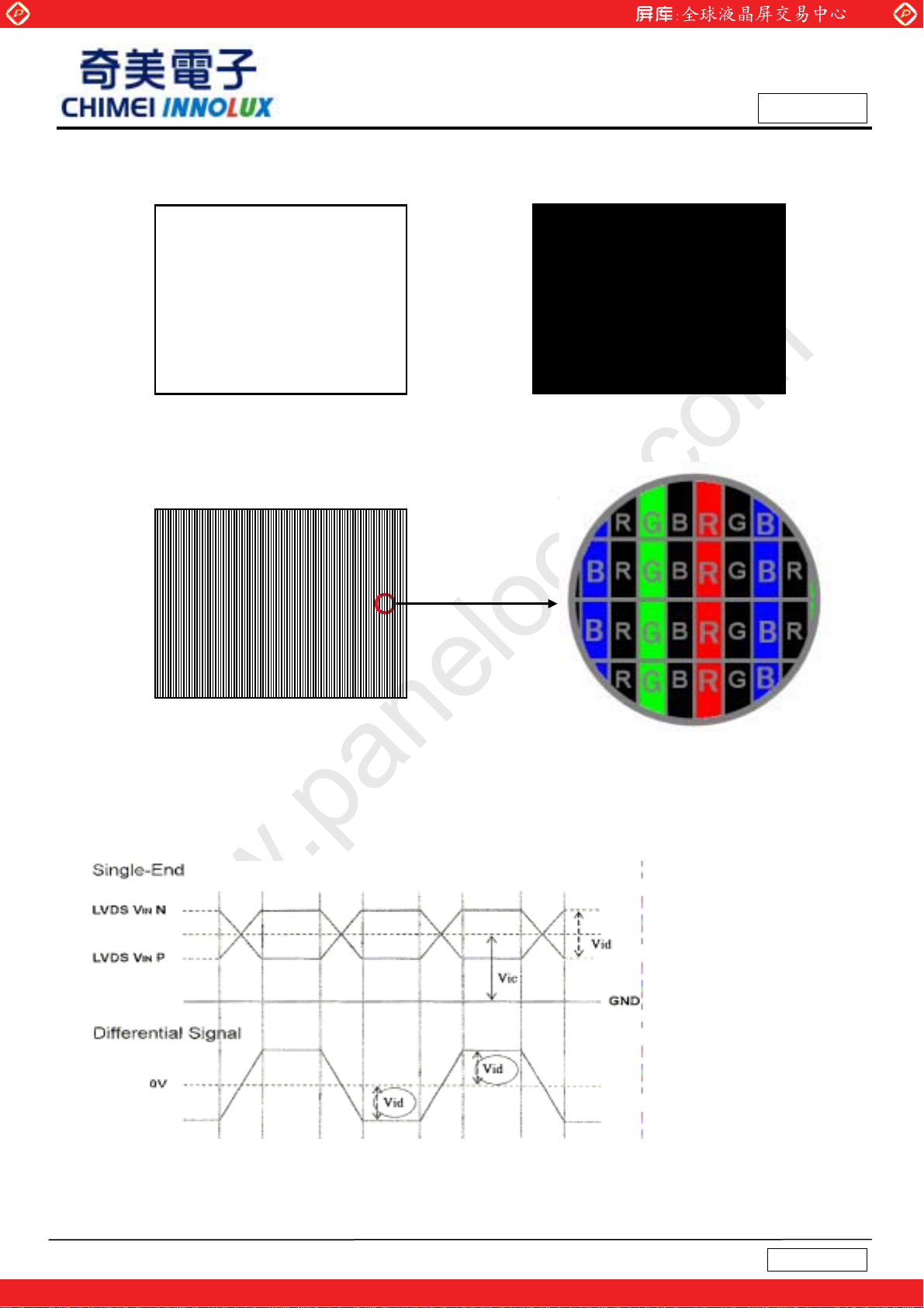
whereas a power dissipation check pattern below is displayed.
www.panelook.com
Issued Date: May. 11, 2010
Model No.: V236H2 - L01
Approval
a. White Pattern
Active Area
c. Vertical Stripe Pattern
b. Black Pattern
Active Area
Active Area
Note (4)The power consumption is specified at the pattern with the maximum current
Note (5) VID waveform condition
8
One step solution for LCD / PDP / OLED panel application: Datasheet, inventory and accessory!
Version 2.0
www.panelook.com
Page 9
Global LCD Panel Exchange Center
≤≤≤
3.1.1 Vcc Power Dip Condition:
www.panelook.com
Issued Date: May. 11, 2010
Model No.: V236H2 - L01
Approval
Vcc
4.0V
4.5V
Td
Dip condition:
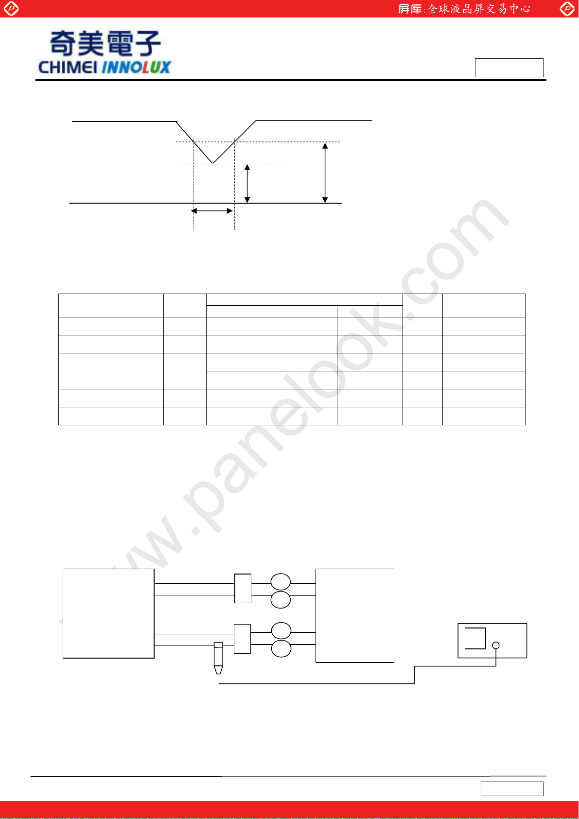
3.2 CCFL (Cold Cathode Fluorescent Lamp) CHARACTERISTICS (Ta = 25 ± 2 к)
Parameter Symbol
Lamp Voltage V
Lamp Current I
W
L
Min. Typ. Max.
972
12.0 12.5 13.0
-- -- 1680 (25 )к
Lamp Turn On Voltage Vs
-- -- 2080 (0 )к
Operating Frequency F
Lamp Life Time L
L
BL
30 -- 80
50000 -- --
Note (1) The waveform of the voltage output of inverter must be area-symmetric and the design of the
inverter must have specifications for the modularized lamp. The performance of the Backlight, such
Value
1080 1188
msTdVVccV 20,5.40.4
Unit Note
IL = 12.5mA
V
RMS
mA
RMS
V
RMS
V
RMS
(2), Ta = 25 к
(2), Ta = 0 к
KHz (3)
Hrs (4)
as lifetime or brightness, is greatly influenced by the characteristics of the DC-AC inverter for the
lamp. All the parameters of an inverter should be carefully designed to avoid producing too much
current leakage from high voltage output of the inverter. When designing or ordering the inverter
please make sure that a poor lighting caused by the mismatch of the Backlight and the inverter
(miss-lighting, flicker, etc.) never occurs. If the above situation is confirmed, the module should be
operated in the same manners when it is installed in your instrument.
HV (Pink)
HV (White)
LCD
Module
Note (2) The lamp starting voltage V
Otherwise the lamp may not be turned on.
HV (Pink)
HV (White)
Current
Probe
1
2
1
2
should be applied to the lamp for more than 1 second after startup.
S
A
A
Inverter
A
A
Oscilloscope
9
One step solution for LCD / PDP / OLED panel application: Datasheet, inventory and accessory!
Version 2.0
www.panelook.com
Page 10

Global LCD Panel Exchange Center
Note (3) The lamp frequency may produce interference with horizontal synchronous frequency of the
display input signals, and it may result in line flow on the display. In order to avoid interference, the
lamp frequency should be detached from the horizontal synchronous frequency and its harmonics
as far as possible.
Note (4) The life time of a lamp is defined as when the brightness is larger than 50% of its original value
and the effective discharge length is longer than 80% of its original length (Effective discharge
length is defined as an area that has equal to or more than 70% brightness compared to the
brightness at the center point of lamp.) as the time in which it continues to operate under the
www.panelook.com
Issued Date: May. 11, 2010
Model No.: V236H2 - L01
Approval
condition at Ta = 25 ±2 and Iк
= 12.0~13.0 mArms.
L
10
One step solution for LCD / PDP / OLED panel application: Datasheet, inventory and accessory!
Version 2.0
www.panelook.com
Page 11

Global LCD Panel Exchange Center
4. BLOCK DIAGRAM
4.1 TFT LCD MODULE
www.panelook.com
Issued Date: May. 11, 2010
Model No.: V236H2 - L01
Approval
RXO0(+/-)
RXO1(+/-)
RXO2(+/-)
RXO3(+/-)
RXOC(+/-)
RXE0(+/-)
RXE1(+/-)
RXE2(+/-)
RXE3(+/-)
RXEC(+/-)
NC
Vcc (5V)
GND
V
L
(STARCONN 093G30-B0001A)
(STM MSAKT2407P30HA)
(P-TWO 187053-30091)
LAMP CONNECTOR
(JST, BDAMR-02VAS-3)
Cvilux CP0404S0000)
(
INPUT CONNECTOR
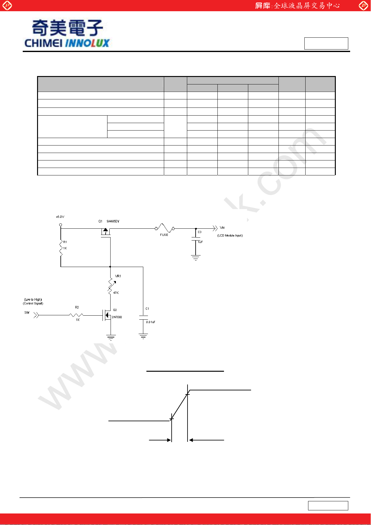
Inverter (W/O)
Lamp Connector
4.2 BACKLIGHT UNIT
SCAN DRIVER IC
TFT LCD PANEL
(1920x3x1080)
TIMING
CONTROLLER
DATA DRIVER IC
DC/DC CONVERTER &
REFERENCE VOLTAGE
BACKLIGHT UNIT
Cvilux CP0404S0000 or equivalent
Note: On the same side, the same polarity lamp voltage design for lamps is recommended.
11
One step solution for LCD / PDP / OLED panel application: Datasheet, inventory and accessory!
Version 2.0
www.panelook.com
Page 12

Global LCD Panel Exchange Center
y
p
(
)
p
)
5. INPUT TERMINAL PIN ASSIGNMENT
5.1 TFT LCD MODULE
Pin No. S
1 RXO02 RXO0+
3 RXO14 RXO1+
5 RXO26 RXO2+
7 GND
8 RXOC-
9 RXOC+
10 RXO311 RXO 3 +
12 RXE013 RXE0+
14 GND
15 RXE116 RXE1+
17 GND
18 RXE219 RXE2+
20 RXEC-
22 RXE323 RXE3+
24 GND
25 NC
26 NC
27 NC
28 VCC
29 VCC
30 VCC
Note (1) Connector Part No.: STM MSAKT2407P30HA or Starconn 093G30-B0001A or
mbol
Negative LVDS differential data input. Channel E0 (even)
Negative LVDS differential data input. Channel E1 (even)
Negative LVDS differential data input. Channel E2 (even)
+
Negative LVDS differential data input. Channel E3 (even)
www.panelook.com
Issued Date: May. 11, 2010
Model No.: V236H2 - L01
Description
Negative LVDS differential data input. Channel O0 (odd)
Positive LVDS differential data in
Negative LVDS differential data input. Channel O1 (odd)
Positive LVDS differential data input. Channel O1 (odd)
Negative LVDS differential data input. Channel O2 (odd)
Positive LVDS differential data input. Channel O2 (odd)
Ground
Negative LVDS differential clock input. (odd)
Positive LVDS differential clock input. (odd)
Negative LVDS differential data input. Channel O3(odd)
Positive LVDS differential data input. Channel O3 (odd)
Positive LVDS differential data input. Channel E0 (even)
Ground
Positive LVDS differential data input. Channel E1 (even)
Ground
Positive LVDS differential data input. Channel E2 (even)
Negative LVDS differential clock input. (even)
Positive LVDS differential clock in
Positive LVDS differential data input. Channel E3 (even)
Ground
For LCD internal use only. Do not connection
For LCD internal use only. Do not connection
For LCD internal use only. Do not connection
Power supply: +5V
Power supply: +5V
Power supply: +5V
ut. Channel O0
ut.(even
odd
Approval
P-TWO 187053-30091 or equivalent
Note (2) The first pixel is odd.
Note (3) Input signal of even and odd clock should be the same timing.
12
One step solution for LCD / PDP / OLED panel application: Datasheet, inventory and accessory!
Version 2.0
www.panelook.com
Page 13

Global LCD Panel Exchange Center
5.2 LVDS DATA MAPPING TABLE
www.panelook.com
Issued Date: May. 11, 2010
Model No.: V236H2 - L01
Approval
LVDS Channel O0
LVDS Channel O1
LVDS Channel O2
LVDS Channel O3
LVDS Channel E0
LVDS Channel E1
LVDS Channel E2
LVDS Channel E3
LVDS output D7 D6 D4 D3 D2 D1 D0
Data order OG0 OR5 OR4 OR3 OR2 OR1 OR0
LVDS output D18 D15 D14 D13 D12 D9 D8
Data order OB1 OB0 OG5 OG4 OG3 OG2 OG1
LVDS output D26 D25 D24 D22 D21 D20 D19
Data order DE NA NA OB5 OB4 OB3 OB2
LVDS output D23 D17 D16 D11 D10 D5 D27
Data order NA OB7 OB6 OG7 OG6 OR7 OR6
LVDS output D7 D6 D4 D3 D2 D1 D0
Data order EG0 ER5 ER4 ER3 ER2 ER1 ER0
LVDS output D18 D15 D14 D13 D12 D9 D8
Data order EB1 EB0 EG5 EG4 EG3 EG2 EG1
LVDS output D26 D25 D24 D22 D21 D20 D19
Data order DE NA NA EB5 EB4 EB3 EB2
LVDS output D23 D17 D16 D11 D10 D5 D27
Data order NA EB7 EB6 EG7 EG6 ER7 ER6
5.3 BACKLIGHT UNIT
Pin Symbol Description Remark
1-1 HV High Voltage Pink
1-2 HV High Voltage White
2-3 HV High Voltage Pink
2-4 HV High Voltage White
Note (1) Connector Part No.: Cvilux CP0404S0000or equivalent
13
One step solution for LCD / PDP / OLED panel application: Datasheet, inventory and accessory!
Version 2.0
www.panelook.com
Page 14

Global LCD Panel Exchange Center
5.4 COLOR DATA INPUT ASSIGNMENT
The brightness of each primary color (red, green and blue) is based on the 8-bit gray scale data input for the
color. The higher the binary input, the brighter the color. The table below provides the assignment of color
versus data input.
Color
R7 R6 R5 R4 R3 R2 R1 R0 G7 G6 G5 G4 G3 G2 G1 G0 B7 B6 B5 B4 B3 B2 B1 B0
Black
Red
Green
Basic
Colors
Gray
Scale
Of
Red
Gray
Scale
Of
Green
Gray
Scale
Of
Blue
Note (1) 0: Low Level Voltage, 1: High Level Voltage
Blue
Cyan
Magenta
Yellow
White
Red(0) / Dark
Red(1)
Red(2)
:
:
Red(253)
Red(254)
Red(255)
Green(0) / Dark
Green(1)
Green(2)
:
:
Green(253)
Green(254)
Green(255)
Blue(0) / Dark
Blue(1)
Blue(2)
:
:
Blue(253)
Blue(254)
Blue(255)
0
0
1
1
0
0
0
0
0
0
1
1
1
1
1
1
0
0
0
0
0
0
:
:
:
:
1
1
1
1
1
1
0
0
0
0
0
0
:
:
:
:
0
0
0
0
0
0
0
0
0
0
0
0
:
:
:
:
0
0
0
0
0
0
Red Green Blue
0
0
1
1
0
0
0
0
0
0
1
1
1
1
1
1
0
0
0
0
0
0
:
:
:
:
1
1
1
1
1
1
0
0
0
0
0
0
:
:
:
:
0
0
0
0
0
0
0
0
0
0
0
0
:
:
:
:
0
0
0
0
0
0
www.panelook.com
0
0
0
0
0
0
1
1
1
1
0
0
0
0
0
0
1
1
0
0
0
0
0
0
0
0
0
0
1
1
1
1
1
1
0
0
1
1
1
1
1
1
1
1
1
1
1
1
0
0
0
0
0
0
0
0
0
1
0
0
0
0
1
0
0
0
:
:
:
:
:
:
:
:
:
:
:
:
1
1
0
1
0
0
1
1
1
0
0
0
1
1
1
1
0
0
0
0
0
0
0
0
0
0
0
0
0
0
0
0
0
0
0
0
:
:
:
:
:
:
:
:
:
:
:
:
0
0
0
0
1
1
0
0
0
0
1
1
0
0
0
0
1
1
0
0
0
0
0
0
0
0
0
0
0
0
0
0
0
0
0
0
:
:
:
:
:
:
:
:
:
:
:
:
0
0
0
0
0
0
0
0
0
0
0
0
0
0
0
0
0
0
Data Signal
0
0
0
0
0
0
0
0
1
1
1
1
0
0
0
0
1
1
1
1
0
0
0
0
1
1
1
1
1
1
1
1
0
0
0
0
0
0
0
0
0
0
0
0
:
:
:
:
:
:
:
:
0
0
0
0
0
0
0
0
0
0
0
0
0
0
0
0
0
0
0
0
0
0
0
0
:
:
:
:
:
:
:
:
1
1
1
1
1
1
1
1
1
1
1
1
0
0
0
0
0
0
0
0
0
0
0
0
:
:
:
:
:
:
:
:
0
0
0
0
0
0
0
0
0
0
0
0
Issued Date: May. 11, 2010
Model No.: V236H2 - L01
Approval
0
0
0
0
0
0
0
0
0
0
0
0
0
0
0
0
0
0
0
0
1
1
0
0
0
0
0
0
0
0
0
0
1
1
1
1
1
1
1
1
1
1
1
1
1
1
1
1
1
1
0
0
1
1
1
1
1
1
1
1
1
1
0
0
0
0
0
0
0
0
1
1
1
1
1
1
1
1
1
1
0
0
0
0
0
0
0
0
0
0
0
0
0
0
0
0
0
0
0
0
0
0
0
0
0
0
0
0
0
0
:
:
:
:
:
:
:
:
:
:
:
:
:
:
:
:
:
:
:
:
0
0
0
0
0
0
0
0
0
0
0
0
0
0
0
0
0
0
0
0
0
0
0
0
0
0
0
0
0
0
0
0
0
0
0
0
0
0
0
0
0
1
0
0
0
0
0
0
0
0
1
0
0
0
0
0
0
0
0
0
:
:
:
:
:
:
:
:
:
:
:
:
:
:
:
:
:
:
:
:
0
1
0
0
0
0
0
0
0
0
1
0
0
0
0
0
0
0
0
0
1
1
0
0
0
0
0
0
0
0
0
0
0
0
0
0
0
0
0
0
0
0
0
0
0
0
0
0
0
1
0
0
0
0
0
0
0
0
1
0
:
:
:
:
:
:
:
:
:
:
:
:
:
:
:
:
:
:
:
:
0
0
1
1
1
1
1
1
0
1
0
0
1
1
1
1
1
1
1
0
0
0
1
1
1
1
1
1
1
1
14
One step solution for LCD / PDP / OLED panel application: Datasheet, inventory and accessory!
Version 2.0
www.panelook.com
Page 15

Global LCD Panel Exchange Center
www.panelook.com
6. INTERFACE TIMING
6.1 INPUT SIGNAL TIMING SPECIFICATIONS
The input signal timing specifications are shown as the following table and timing diagram.
The input signal timing specifications are shown as the following table and timing diagram.
Signal Item Symbol Min. Typ. Max. Unit Note
Frequency Fc 58.54 74.25 98 MHz
Period Tc - 13.47 - ns
Issued Date: May. 11, 2010
Model No.: V236H2 - L01
Approval
LVDS Clock
LVDS D a ta
Vertical Active Display Term
Input cycle to
cycle jitter
Spread
spectrum
modulation
range
Spread
spectrum
modulation
frequency
High Time Tch - 4/7 - Tc -
Low Time Tcl - 3/7 - Tc -
Setup Time Tlvs 600 - - ps
Hold Time Tlvh 600 - - ps
Frame Rate Fr 50 60 75 Hz Tv=Tvd+Tvb
Total Tv 1115 112 5 1136 Th -
Display Tvd 1080 1080 1080 Th -
T
rcl
clkin_mod
F
F
- - 200 KHz
SSM
-
0.98*Fc - 1.02*Fc MHz
-
200
ps (1)
(2)
(3)
Blank Tvb Tv-Tvd 45 Tv-Tvd Th -
Total Th 1050 1100 1150 Tc Th=Thd+Thb
Horizontal Active Display Term
Note: Because this module is operated by DE only mode, Hsync and Vsync input signals are ignored.
Display Thd 960 960 960 Tc -
Blank Thb Th-Thd 140 Th-Thd Tc -
15
Version 2.0
One step solution for LCD / PDP / OLED panel application: Datasheet, inventory and accessory!
www.panelook.com
Page 16

Global LCD Panel Exchange Center
DE
DCLK
T
C
DE
www.panelook.com
INPUT SIGNAL TIMING DIAGRAM
Th
hd
Thb
T
Issued Date: May. 11, 2010
Model No.: V236H2 - L01
Approval
DATA
Note (1) The input clock cycle-to-cycle jitter is defined as below figures. Trcl = I T1 – TI
T1
Note (2) The SSCG (Spread spectrum clock generator) is defined as below figures.
T2
Note (3) The LVDS timing diagram and setup/hold time is defined and showing as the following figures.
16
One step solution for LCD / PDP / OLED panel application: Datasheet, inventory and accessory!
Version 2.0
www.panelook.com
Page 17

Global LCD Panel Exchange Center
LVDS RECEIVER INTERFACE TIMING DIAGRAM
RXCLK+/-
RXn+/-
Tlvs
www.panelook.com
Issued Date: May. 11, 2010
Model No.: V236H2 - L01
Approval
Tc
Tlvh
1
14
T
c
3
14
T
c
5
14
T
c
7
14
T
c
9
14
T
c
11
T
14
c
c
T
13
14
6.2 POWER ON/OFF SEQUENCE
To prevent a latch-up or DC operation of LCD module, the power on/off sequence should be as the
diagram below.
- Power Supply
for LCD, Vcc
0V
90%
10%
t1
90%
t4
10%
t7
10%
t3t2
- Interface Signal
(LVDS Signal of
Transmitter), V
- Power for Backlight
I
0V
Valid Data
t6t5
50%50%
ONOFF OFF
17
One step solution for LCD / PDP / OLED panel application: Datasheet, inventory and accessory!
Version 2.0
www.panelook.com
Page 18

Global LCD Panel Exchange Center
Timing Specifications:
0.5< t1 Љ 10 msec
0 < t2 Љ 50 msec
0 < t3 Љ 50 msec
t4 Њ 500 msec
t5 Њ 450 msec
t6 Њ 90 msec
5< t7 Љ 100 msec
Note.
(1) The supply voltage of the external system for the module input should be the same as the definition of Vcc.
(2) Apply the lamp voltage within the LCD operation range. When the backlight turns on before the LCD operation
of the LCD turns off, the display may momentarily become abnormal screen.
www.panelook.com
Issued Date: May. 11, 2010
Model No.: V236H2 - L01
Approval
(3) In case of VCC = off level, please keep the level of input signals on the low or keep a high impedance.
(4) T4 should be measured after the module has been fully discharged between power off and on period.
(5) Interface signal shall not be kept at high impedance when the power is on.
(6) CMO won’t take any responsibility for the products which are damaged by the customers not following the
Power Sequence.
(7) It is suggested that Vcc falling time follows t7 specification, else slight noise is likely to occur when LCD is
turned off (even backlight is already off).
18
One step solution for LCD / PDP / OLED panel application: Datasheet, inventory and accessory!
Version 2.0
www.panelook.com
Page 19

Global LCD Panel Exchange Center
7. OPTICAL CHARACTERISTICS
7.1 TEST CONDITIONS
Item Symbol Value Unit
Ambient Temperature Ta 25±2
Ambient Humidity Ha 50±10 %RH
Supply Voltage VCC 5 V
Input Signal According to typical value in "3. ELECTRICAL CHARACTERISTICS"
Lamp Current IL 12.5±0.5 mA
Inverter Operating Frequency FL 58±3 KHz
Inverter Logah F236H1-2UA-L001
7.2 OPTICAL SPECIFICATIONS
Item Symbol Condition Min. Typ. Max. Unit Note
www.panelook.com
Issued Date: May. 11, 2010
Model No.: V236H2 - L01
Approval
o
C
Contrast Ratio CR 600 800 - (2)
Response Time
Center Luminance of White L
T
R
T
F
C
- 1.5 2.5
ms (3)
- 3.5 5.5
240 300 - - (4)
White Variation δW - - 1.33 - (7)
Cross Talk CT - - 4 % (5)
θ
=0° , θY =0°
x
Viewing Angle at
Normal Direction
CR≥10
-
-
-
-
-
-
-
-
Typ.
-0.03
0.642
0.331
0.265
0.602
0.150
0.063
0.280
0.288
Typ.
+0.03
68 72 - %
140 160
130 150
Deg. (1)
-
(6)
NTSC
Ratio
Color
Chromaticity
Viewing
Angle
Red
Rx
Ry
Gx
Green
Gy
Bx
Blue
By
Wx
White
Wy
Color Gamut CG
Horizontal
Vertical θ
θ
x+θx
Y+θY
-
-
Note (1) Definition of Viewing Angle (θx, θy):
Viewing angles are measured by Autronic Conoscope Cono-80
19
One step solution for LCD / PDP / OLED panel application: Datasheet, inventory and accessory!
Version 2.0
www.panelook.com
Page 20

Global LCD Panel Exchange Center
www.panelook.com
Issued Date: May. 11, 2010
Model No.: V236H2 - L01
Approval
Normal
θx = θy = 0
θy- θy+
θX- = 90
6 o’clock
θ
y- = 90
x-
y-
Note (2) Definition of Contrast Ratio (CR):
The contrast ratio can be calculated by the following expression.
Contrast Ratio (CR) = L255 / L0
L255: Luminance of gray level 255
L 0: Luminance of gray level 0
CR = CR (5),
CR (X) is corresponding to the Contrast Ratio of the point X at the figure in Note (7).
θx−
θx+
y+
12 o’clock direction
θ
y+ = 90
θX+ = 90
x+
Note (3) Definition of Response Time (T
Gray Level 255
100%
90%
Optical
Response
10%
0%
R
T
, TF):
R
Note (4) Definition of Luminance of White (L
Measure the luminance of gray level 255 at center point and 5 points
= L (5)
L
C
):
C
Gray Level 0
20
T
Gray Level 255
F
Time
One step solution for LCD / PDP / OLED panel application: Datasheet, inventory and accessory!
Version 2.0
www.panelook.com
Page 21

Global LCD Panel Exchange Center
A
A
L (X) is corresponding to the luminance of the point X at the figure in Note (7).
Note (5) Definition of Cross Talk (CT):
www.panelook.com
Issued Date: May. 11, 2010
Model No.: V236H2 - L01
Approval
CT = | Y
– YA | / YA× 100 (%)
B
Where:
Y
= Luminance of measured location without gray level 0 pattern (cd/m2)
A
= Luminance of measured location with gray level 0 pattern (cd/m2)
Y
B
ctive Area
Gray 128
Y
(D/8,W/2)
A, L
Y
(D/2,7W/8)
A, D
(0, 0)
Note (6) Measurement Setup:
The LCD module should be stabilized at given temperature for 1 hour to avoid abrupt temperature
change during measuring. In order to stabilize the luminance, the measurement should be executed
after lighting Backlight for 1 hour in a windless room.
Y
A, U
Y
A, R
(D,W)
(D/2,W/8)
(7D/8,W/2)
(D/4,W/4)
(D/8,W/2)
Y
B, L
Y
(D/2,7W/8)
B, D
(0, 0)
ctive Area
Gray 0
Gray 128
Y
(D/2,W/8)
B, U
Y
(7D/8,W/2)
B, R
(3D/4,3W/4)
(D,W)
Note (7) Definition of White Variation (δW):
Measure the luminance of gray level 255 at 5 points
δW = Maximum [L (1), L (2), L (3), L (4), L (5)] / Minimum [L (1), L (2), L (3), L (4), L (5)]
21
One step solution for LCD / PDP / OLED panel application: Datasheet, inventory and accessory!
Version 2.0
www.panelook.com
Page 22

Global LCD Panel Exchange Center
www.panelook.com
Issued Date: May. 11, 2010
Model No.: V236H2 - L01
Approval
Horizontal Line
D
D/4 D/2 3D/4
W/4
W/2
W
Vertical Line
3W/4
1 2
X
5
3 4
Active Area
: Test Point
X=1 to 5
22
One step solution for LCD / PDP / OLED panel application: Datasheet, inventory and accessory!
Version 2.0
www.panelook.com
Page 23

Global LCD Panel Exchange Center
8. DEFINITION OF LABELS
8.1 CMO MODULE LABEL
The barcode nameplate is pasted on each module as illustration, and its definitions are as following explanation.
V236H2-L01 Rev. XX
www.panelook.com
Issued Date: May. 11, 2010
Model No.: V236H2 - L01
Approval
E207943
CHI MEI
OPTOELECTRONICS
X X X X X X X Y M D L N N N N
MADE IN TAIWAN
GEMN
RoHS
V236H2-L01 Rev. XX
CHI MEI
OPTOELECTRONICS
X X X X X X X Y M D L N N N N
E207943
MADE IN TAIWAN
MADE IN CHINA
LEOO(or CAPG or CANO)
RoHS
(a) Model Name: V236H2-L01
(b) Revision: Rev. XX, for example: A0, A1… B1, B2… or C1, C2…etc.
(c) Serial ID: X X
X X X X X Y M D L N N N N
Serial No.
Product Line
Year, Month, Date
CMO Internal Use
CMO Internal Use
Serial ID includes the information as below:
Manufactured Date: Year: 2001=1,2002=2,2003=3,2004=4…2010=0,2011=1,2012=2..
ʳ Month: 1~9, A~C, for Jan. ~ Dec.
ʳ Day: 1~9, A~Y, for 1st to 31st, exclude I ,O, and U.
(a) Revision Code: Cover all the change
(b) Serial No.: Manufacturing sequence of product
(c) Product Line: 1 -> Line1, 2 -> Line 2, …etc.
Revision
CMO Internal Use
23
One step solution for LCD / PDP / OLED panel application: Datasheet, inventory and accessory!
Version 2.0
www.panelook.com
Page 24

Global LCD Panel Exchange Center
9. PACKAGING
9.1 PACKING SPECIFICATIONS
(1) 5 LCD TV modules / 1 Box
(2)
Box dimensions : 642(L)x376(W)x390(H)mm
(3) Weight : Approx. 14.5Kg(5 modules per carton)
9.2 PACKING METHOD
Figures 9-1 and 9-2 are the packing method
LCD TV Module
www.panelook.com
Issued Date: May. 11, 2010
Model No.: V236H2 - L01
Approval
Anti-Static Bag
Cushion(Bottom)
Carton
Module*5pcs
Cushion(Top)
Carton Label
Figure.9-1 Packing Method
24
One step solution for LCD / PDP / OLED panel application: Datasheet, inventory and accessory!
Version 2.0
www.panelook.com
Page 25

Global LCD Panel Exchange Center
www.panelook.com
Issued Date: May. 11, 2010
Model No.: V236H2 - L01
Approval
Sea / Land Transportation
(40ft HQ / 40ft Container)
Air Transportation
Figure.9-2 packing method
25
One step solution for LCD / PDP / OLED panel application: Datasheet, inventory and accessory!
Version 2.0
www.panelook.com
Page 26

Global LCD Panel Exchange Center
www.panelook.com
Issued Date: May. 11, 2010
Model No.: V236H2 - L01
Approval
10. PRECAUTIONS
10.1 ASSEMBLY AND HANDLING PRECAUTIONS
(1) Do not apply rough force such as bending or twisting to the module during assembly.
(2) It is recommended to assemble or to install a module into the user’s system in clean working areas. The
dust and oil may cause electrical short or worsen the polarizer.
(3) Do not apply pressure or impulse to the module to prevent the damage of LCD panel and backlight.
(4) Always follow the correct power-on sequence when the LCD module is turned on. This can prevent the
damage and latch-up of the CMOS LSI chips.
(5) Do not plug in or pull out the I/F connector while the module is in operation.
(6) Do not disassemble the module.
(7) Use a soft dry cloth without chemicals for cleaning, because the surface of polarizer is very soft and
easily scratched.
(8) Moisture can easily penetrate into LCD module and may cause the damage during operation.
(9) High temperature or humidity may deteriorate the performance of LCD module. Please store LCD
modules in the specified storage conditions.
(10) When ambient temperature is lower than 10к, the display quality might be reduced. For example, the
response time will become slow, and the starting voltage of CCFL will be higher than that of room
temperature.
10.2 SAFETY PRECAUTIONS
(1) The startup voltage of a backlight is over 1000 Volts. It may cause an electrical shock while assembling
with the inverter. Do not disassemble the module or insert anything into the backlight unit.
(2) If the liquid crystal material leaks from the panel, it should be kept away from the eyes or mouth. In case
of contact with hands, skin or clothes, it has to be washed away thoroughly with soap.
(3) After the module’s end of life, it is not harmful in case of normal operation and storage.
10.3 SAFETY STANDARDS
The LCD module should be certified with safety regulations as follows:
(1) UL60950-1 or updated standard.
(2) IEC60950-1 or updated standard.
(3) UL60065 or updated standard.
(4) IEC60065 or updated standard.
26
One step solution for LCD / PDP / OLED panel application: Datasheet, inventory and accessory!
Version 2.0
www.panelook.com
Page 27

Global LCD Panel Exchange Center
11. MECHANICAL CHARACTERISTIC
www.panelook.com
Issued Date: May. 11, 2010
Model No.: V236H2 - L01
Approval
27
One step solution for LCD / PDP / OLED panel application: Datasheet, inventory and accessory!
Version 2.0
www.panelook.com
Page 28

Global LCD Panel Exchange Center
www.panelook.com
Issued Date: May. 11, 2010
Model No.: V236H2 - L01
Approval
28
One step solution for LCD / PDP / OLED panel application: Datasheet, inventory and accessory!
Version 2.0
www.panelook.com
Page 29

Global LCD Panel Exchange Center
www.panelook.com
Issued Date: May. 11, 2010
Model No.: V236H2 - L01
Approval
29
One step solution for LCD / PDP / OLED panel application: Datasheet, inventory and accessory!
Version 2.0
www.panelook.com
 Loading...