

Page 1
Global LCD Panel Exchange Center
MODEL NO.: V236H1
www.panelook.com
PRODUCT SPECIFICATION
□ Tentative Specification
□ Preliminary Specification
■ Approval Specification
SUFFIX: L03
Customer:
APPROVED BY SIGNATURE
Name / Title
Note
Please return 1 copy for your confirmation with your
signature and comments.
Approved By Checked By Prepared By
Chao-Chun Chung Roger Huang Bowei Huang
Version 2.0 1 Date
The copyright belongs to CHIMEI InnoLux. Any unauthorized use is prohibited
One step solution for LCD / PDP / OLED panel application: Datasheet, inventory and accessory!
ΚΚΚΚ
03 Jun 2011
www.panelook.com
Page 2

Global LCD Panel Exchange Center
www.panelook.com
PRODUCT SPECIFICATION
CONTENTS
1. GENERAL DESCRIPTION................................................................................................................................................... 5
1.1 OVERVIEW....................................................................................................................................................5
1.2 FEATURES ....................................................................................................................................................5
1.3 APPLICATION................................................................................................................................................5
1.4 GENERAL SPECIFICATIONS ........................................................................................................................5
1.5 MECHANICAL SPECIFICATIONS ..................................................................................................................6
2. ABSOLUTE MAXIMUM RATINGS ....................................................................................................................................7
2.1 ABSOLUTE RATINGS OF ENVIRONMENT....................................................................................................7
2.2 PACKAGE STORAGE ....................................................................................................................................8
2.3 ELECTRICAL ABSOLUTE RATINGS..............................................................................................................8
2.3.1 TFT LCD MODULE...............................................................................................................................8
2.3.2 BACKLIGHT UNIT................................................................................................................................8
3. ELECTRICAL CHARACTERISTICS ................................................................................................................................... 9
3.1 TFT LCD MODULE.........................................................................................................................................9
3.2 BACKLIGHT CONNECTOR PIN CONFIGURATION..................................................................................... 11
3.2.1 LAMP SPECIFICATION...................................................................................................................... 11
4. BLOCK DIAGRAM OF INTERFACE................................................................................................................................ 13
4.1 TFT LCD MODULE.......................................................................................................................................13
4.2 BACKLIGHT UNIT........................................................................................................................................ 13
5. INPUT TERMINAL PIN ASSIGNMENT .......................................................................................................................... 14
5.1 TFT LCD Module Input .................................................................................................................................14
5.2 BACKLIGHT UNIT........................................................................................................................................ 15
5.3 BLOCK DIAGRAM OF INTERFACE .............................................................................................................16
5.4 LVDS INTERFACE .......................................................................................................................................18
5.5 COLOR DATA INPUT ASSIGNMENT............................................................................................................19
6. INTERFACE TIMING......................................................................................................................................................... 20
6.1 INPUT SIGNAL TIMING SPECIFICATIONS..................................................................................................20
6.2 POWER ON/OFF SEQUENCE.....................................................................................................................22
7. OPTICAL CHARACTERISTICS ........................................................................................................................................ 23
7.1 TEST CONDITIONS .....................................................................................................................................23
7.2 OPTICAL SPECIFICATIONS ........................................................................................................................24
Version 2.0 2 Date
The copyright belongs to CHIMEI InnoLux. Any unauthorized use is prohibited
One step solution for LCD / PDP / OLED panel application: Datasheet, inventory and accessory!
ΚΚΚΚ
03 Jun 2011
www.panelook.com
Page 3
Global LCD Panel Exchange Center
www.panelook.com
PRODUCT SPECIFICATION
8. PRECAUTIONS ..................................................................................................................................................................28
8.1 ASSEMBLY AND HANDLING PRECAUTIONS .............................................................................................28
8.2 SAFETY PRECAUTIONS............................................................................................................................. 28
8.3 SAFETY STANDARDS.................................................................................................................................28
9. DEFINITION OF LABELS.................................................................................................................................................. 29
9.1 CMI MODULE LABEL...................................................................................................................................29
10. PACKAGING .................................................................................................................................................................... 30
10.1 PACKAGING SPECIFICATIONS.................................................................................................................30
10.2 PACKAGING METHOD .............................................................................................................................. 30
11. MECHANICAL CHARACTERISTIC .............................................................................................................................. 32
Version 2.0 3 Date
The copyright belongs to CHIMEI InnoLux. Any unauthorized use is prohibited
One step solution for LCD / PDP / OLED panel application: Datasheet, inventory and accessory!
ΚΚΚΚ
03 Jun 2011
www.panelook.com
Page 4
Global LCD Panel Exchange Center
Version Date Page(New) Section Description
Ver. 2.0 Jun. 03, 2011 All All The Approved specification was first issued.
www.panelook.com
PRODUCT SPECIFICATION
REVISION HISTORY
Version 2.0 4 Date
The copyright belongs to CHIMEI InnoLux. Any unauthorized use is prohibited
One step solution for LCD / PDP / OLED panel application: Datasheet, inventory and accessory!
ΚΚΚΚ
03 Jun 2011
www.panelook.com
Page 5
Global LCD Panel Exchange Center
1. GENERAL DESCRIPTION
1.1 OVERVIEW
V236H1-L03 is a 23.6” TFT Liquid Crystal Display module with 2 U-type CCFL Backlight unit and 30 pins
2ch-LVDS interface. This module supports 1920 x 1080 Full HDTV format and can display 16.7M (6 bit+Hi-FRC)
colors. The inverter module for backlight isn’t built-in.
1.2 FEATURES
Ё
Extra-wide viewing angle.
Ё
High contrast ratio.
Ё
Fast response time.
Ё
High color saturation.
Ё
Full HD (1920 x 1080 pixels) resolution.
Ё
DE (Data Enable) only mode.
www.panelook.com
PRODUCT SPECIFICATION
Ё
LVDS (Low Voltage Differential Signaling) interface.
Ё
RoHS compliance.
1.3 APPLICATION
Ё
Standard Living Room TVs
Ё
MFM Application
1.4 GENERAL SPECIFICATIONS
Item Specification Unit Note
Active Area 521.28H) x 293.22(V) (23.547” diagonal) mm
Bezel Opening Area 525.22 (H) x 297.22 (V) mm
Driver Element a-si TFT active matrix - -
Pixel Number 1920 x R.G.B. x 1080 pixel -
Pixel Pitch 0.2715(H) x 0.2715(V) mm -
Pixel Arrangement RGB vertical stripe - -
Power consumption 32.1W (LVDS input Power 5.1W + CCFL Backlight Power 27 W) Watt (2)
Display Colors 16.7M (6 bit+Hi-FRC) color -
(1)
Display Operation Mode Transmissive mode / Normally white - -
Surface Treatment Anti-Glare coating (Haze 25%) - (3)
Note (1) Please refer to the attached drawings in chapter 9 for more information about the front and back outlines.
Note (2) Please refer sec 3.1 and 3.2 for more information of Power consumption
Note (3) The spec. of the surface treatment is temporarily for this phase. CMI reserves the rights to change this feature.
Version 2.0 5 Date
The copyright belongs to CHIMEI InnoLux. Any unauthorized use is prohibited
One step solution for LCD / PDP / OLED panel application: Datasheet, inventory and accessory!
ΚΚΚΚ
03 Jun 2011
www.panelook.com
Page 6
Global LCD Panel Exchange Center
1.5 MECHANICAL SPECIFICATIONS
Item Min. Typ. Max. Unit Note
Horizontal (H) 543.8 544.8 545.8 mm (1)
Vertical (V) 319.5 320.5 321.5 mm (1)
Module Size
Depth (D) 45.7 46.7 47.7 mm To Rear
Depth (D) 50.7 51.7 52.7 mm To Boss
Weight - 2400 - g -
Note (1) Please refer to the attached drawings for more information of front and back outline dimensions.
www.panelook.com
PRODUCT SPECIFICATION
Version 2.0 6 Date
The copyright belongs to CHIMEI InnoLux. Any unauthorized use is prohibited
One step solution for LCD / PDP / OLED panel application: Datasheet, inventory and accessory!
ΚΚΚΚ
03 Jun 2011
www.panelook.com
Page 7
Global LCD Panel Exchange Center
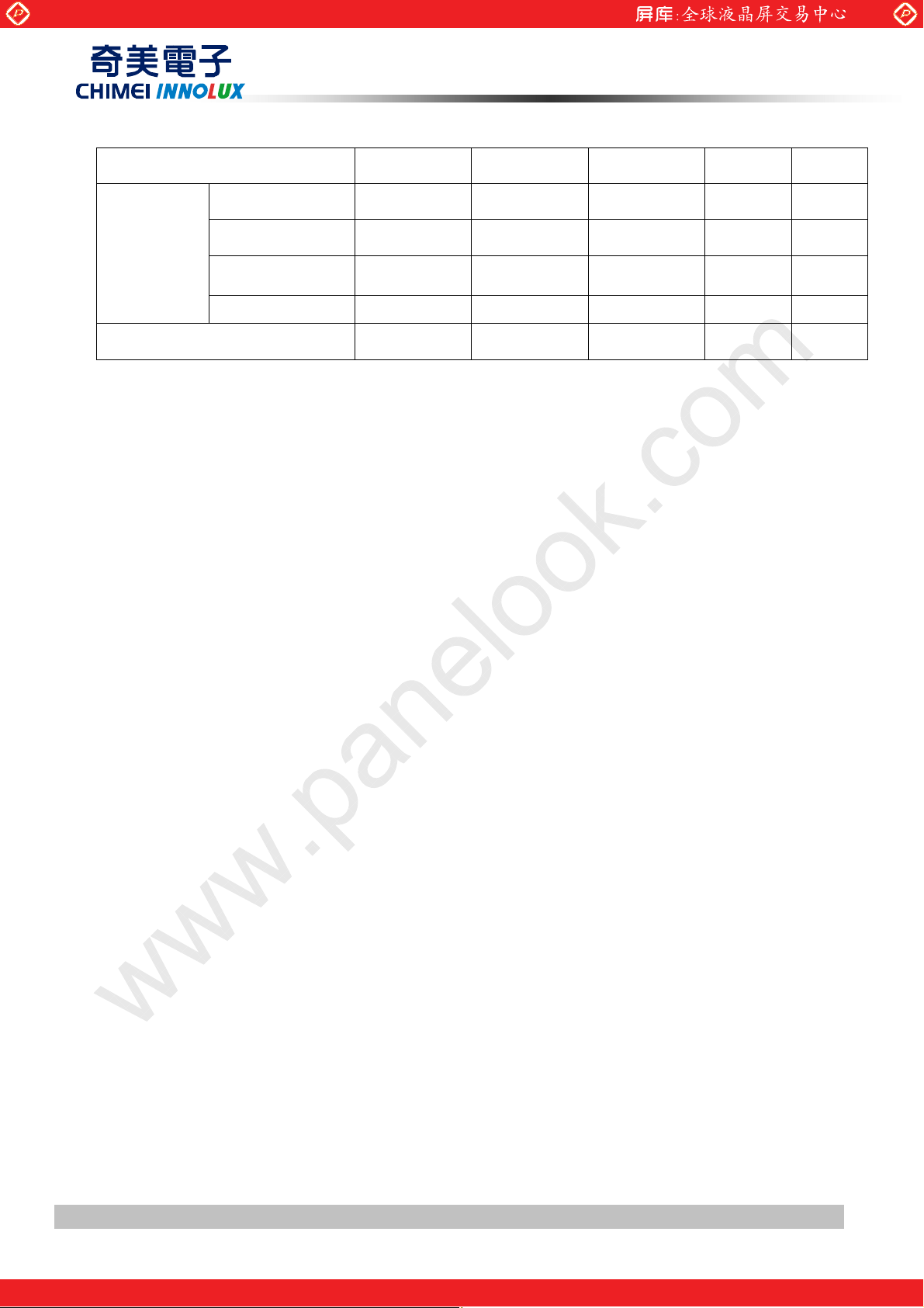
2. ABSOLUTE MAXIMUM RATINGS
2.1 ABSOLUTE RATINGS OF ENVIRONMENT
Item Symbol
Storage Temperature TST -20 +60 ºC (1)
Operating Ambient Temperature TOP 0 50 ºC (1), (2)
Shock (Non-Operating) SNOP - 50 G (3), (5)
Vibration (Non-Operating) VNOP - 1.0 G (4), (5)
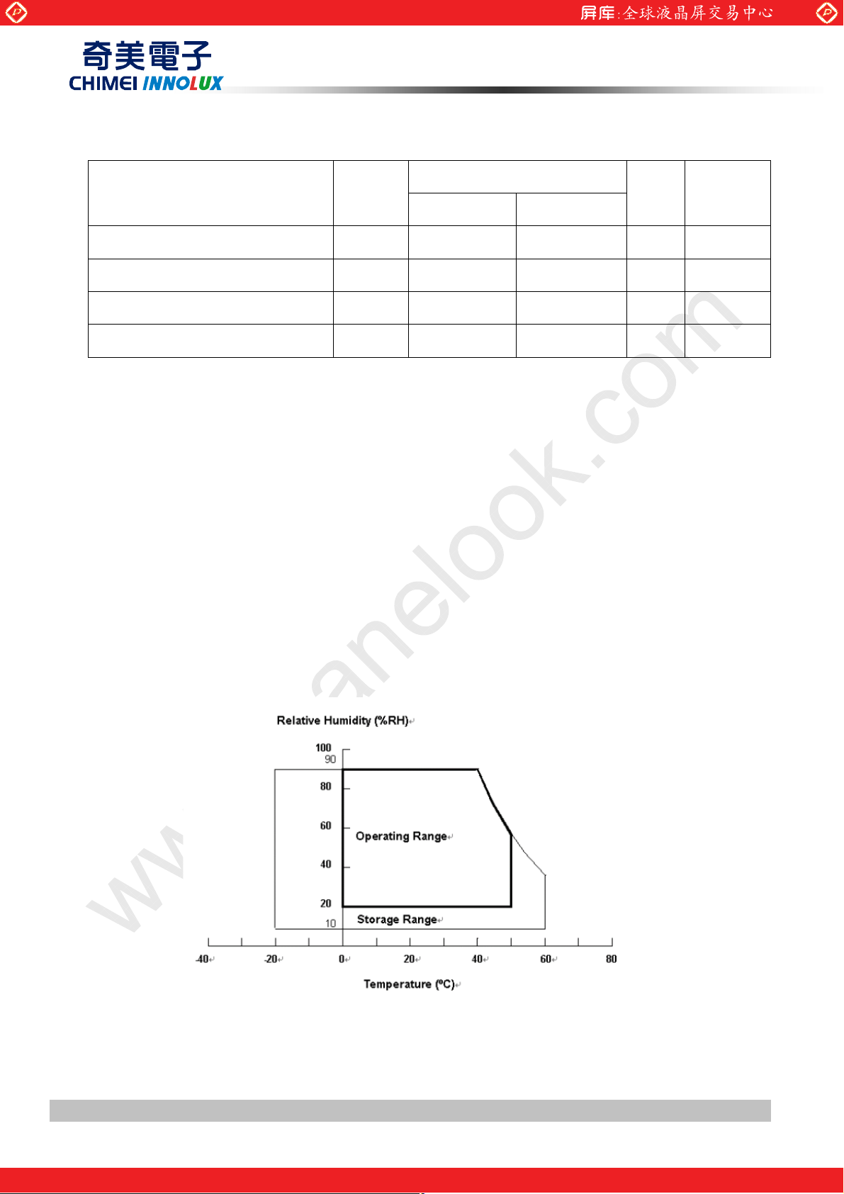
Note (1) Temperature and relative humidity range is shown in the figure below.
www.panelook.com
PRODUCT SPECIFICATION
Value
Unit Note
Min. Max.
(a) 90 %RH Max. (Ta
(b) Wet-bulb temperature should be 39 ºC Max. (Ta > 40 ºC).
(c) No condensation.
Note (2) The maximum operating temperature is based on the test condition that the surface temperature of
display area is less than or equal to 65 ºC with LCD module alone in a temperature controlled chamber.
Thermal management should be considered in final product design to prevent the surface temperature
of display area from being over 65 ºC. The range of operating temperature may degrade in case of
improper thermal management in final product design.
Note (3) 11 ms, half sine wave, 1 time for ± X, ± Y, ± Z.
Note (4) 10 ~ 200 Hz, 10 min, 1 time each X, Y, Z.
Note (5) At testing Vibration and Shock, the fixture in holding the module has to be hard and rigid enough so that
the module would not be twisted or bent by the fixture.
Љ
40 ºC).
Version 2.0 7 Date
The copyright belongs to CHIMEI InnoLux. Any unauthorized use is prohibited
One step solution for LCD / PDP / OLED panel application: Datasheet, inventory and accessory!
ΚΚΚΚ
03 Jun 2011
www.panelook.com
Page 8
Global LCD Panel Exchange Center
2.2 PACKAGE STORAGE
When storing modules as spares for a long time, the following precaution is necessary.
(a) Do not leave the module in high temperature, and high humidity for a long time, It is highly recommended to
www.panelook.com
PRODUCT SPECIFICATION
store the module with temperature from 0 to 35
(b) The module shall be stored in dark place. Do not store the TFT-LCD module in direct sunlight or fluorescent
light.
к
at normal humidity without condensation.
2.3 ELECTRICAL ABSOLUTE RATINGS
2.3.1 TFT LCD MODULE
Value
Item Symbol
Min. Max.
Power Supply Voltage VCC -0.3 +6 V
Logic Input Voltage VIN -0.3 3.6 V
2.3.2 BACKLIGHT UNIT
Value
Item Symbol
Min. Max.
Lamp Voltage VL 981 1188 V
Unit Note
(1)
Unit Note
RMS
Power Supply Voltage VBL 0 30 V (1)
Ё
Control Signal Level
Note (1) Permanent damage to the device may occur if maximum values are exceeded. Function operation
should be restricted to the conditions described under Normal Operating Conditions.
Note (2) No moisture condensation or freezing.
Note (3) The control signals include On/Off Control & E-PWM.
-0.3 7 V (1), (3)
Version 2.0 8 Date
The copyright belongs to CHIMEI InnoLux. Any unauthorized use is prohibited
One step solution for LCD / PDP / OLED panel application: Datasheet, inventory and accessory!
ΚΚΚΚ
03 Jun 2011
www.panelook.com
Page 9
Global LCD Panel Exchange Center
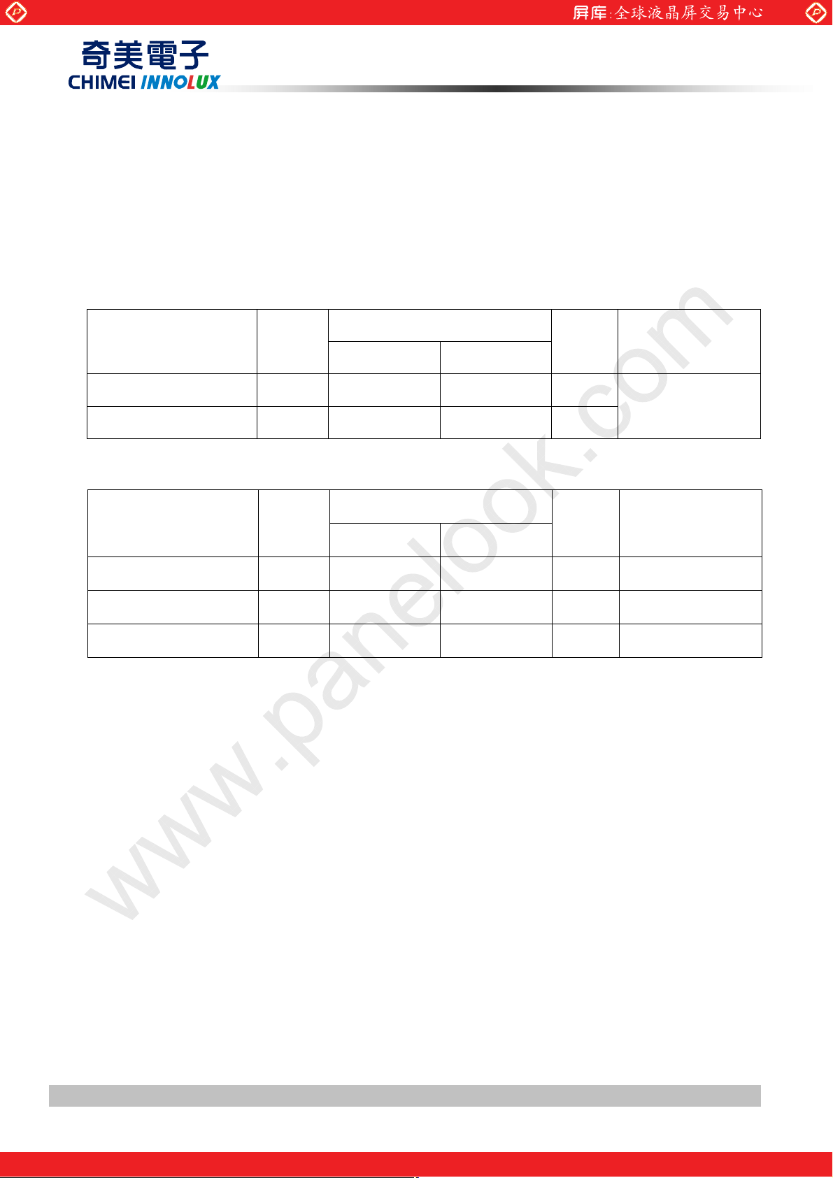
3. ELECTRICAL CHARACTERISTICS
3.1 TFT LCD MODULE
(Ta = 25 ± 2 ºC)
Parameter Symbol
Power Supply Voltage VCC 4.5 5.0 5.5 V (1)
Rush Current I
Power Consumption P
White Pattern
www.panelook.com
PRODUCT SPECIFICATION
Value
Unit Note
Min. Typ. Max.
Ё
RUSH
T
Ё
Ё
Ё
Ё
5.1 6.45 W (3)
0.4 0.55 A
3 A (2)
Power Supply Current
Differential Input High
Threshold Voltage
Differential Input Low
LVDS
interface
Note (1) The module should be always operated within the above ranges.
Threshold Voltage
Common Input Voltage VCM 1.0 1.2 1.4 V
Differential input voltage
(single-end)
Vertical Stripe
Black Pattern
Ё
Ё
V
V
|V
LVT H
LVTL
ID
+100
| 200
Ё
Ё
Ё
0.96 1.29 A
1.02 1.29 A
Ё
Ё
Ё
(4)
Ё
-100 mV
600 mV
mV
(5)
Version 2.0 9 Date
The copyright belongs to CHIMEI InnoLux. Any unauthorized use is prohibited
One step solution for LCD / PDP / OLED panel application: Datasheet, inventory and accessory!
ΚΚΚΚ
03 Jun 2011
www.panelook.com
Page 10
Global LCD Panel Exchange Center
www.panelook.com
PRODUCT SPECIFICATION
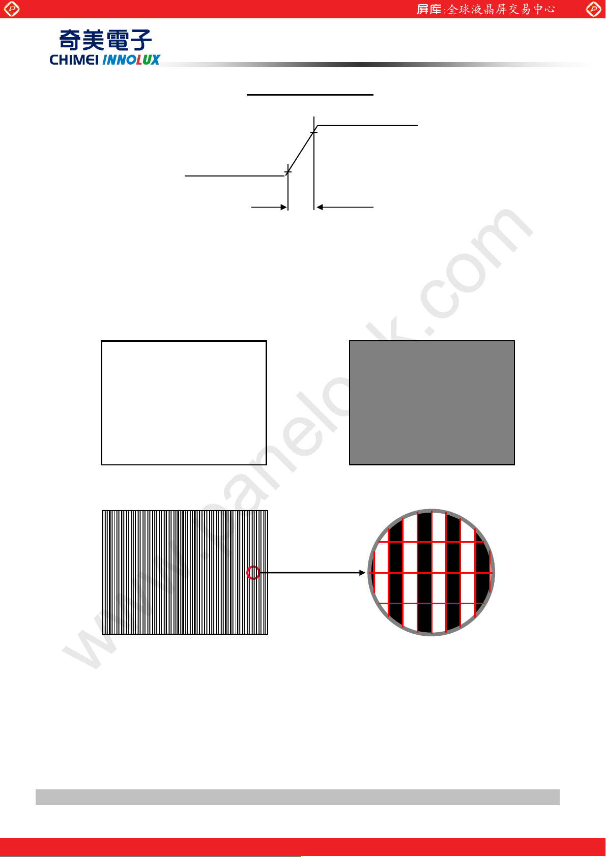
Vcc rising time is 470us
0.9Vcc
0.1Vcc
Vcc
Note (3) The Specified Power consumption is under Vertical Stripe pattern.
Note (4) The specified power supply current is under the conditions at Vcc = 12 V, Ta = 25 ± 2 ºC, f
whereas a power dissipation check pattern below is displayed.
a. White Pattern
Active Area
c. Vertical Stripe Pattern
GND
470us
b. Black Pattern
Active Area
= 60 Hz,
v
Active Area
R
G
R
B
G
R
B
G
R R
G
R
G
B
B
B
B
B
R
G
B
R
R
G
B
R
G
B
Version 2.0 10 Date
The copyright belongs to CHIMEI InnoLux. Any unauthorized use is prohibited
ΚΚΚΚ
03 Jun 2011
One step solution for LCD / PDP / OLED panel application: Datasheet, inventory and accessory!
www.panelook.com
Page 11
Global LCD Panel Exchange Center
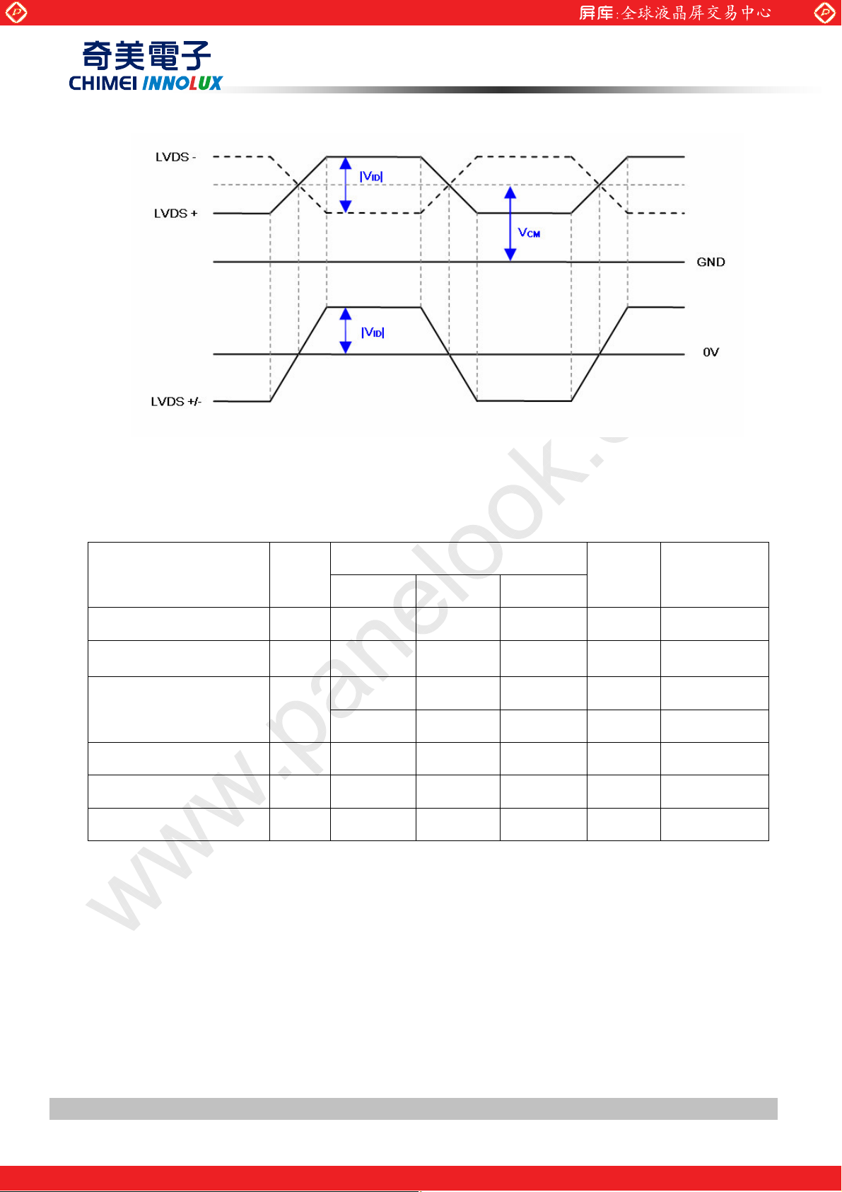
Note (5) The LVDS input characteristics are as follows :
www.panelook.com
PRODUCT SPECIFICATION
3.2 BACKLIGHT CONNECTOR PIN CONFIGURATION
3.2.1 LAMP SPECIFICATION
(Ta = 25 ± 2 ºC)
Value
Parameter Symbol
Min. Typ. Max.
Lamp Input Voltage VL 981 1080 1188 V
Lamp Current IL 12.0 12.5 13.0 mA
- - 1910 V
Lamp Turn On Voltage VS
- - 1730 V
Operating Frequency FO 30 - 80 KHz (2)
Lamp Life Time LBL 50,000 - - Hrs (3)
Power Consumption PBL - 27 - W
Unit Note
I
RMS
RMS
(1) , Ta = 0 ºC
RMS
(1) , Ta = 25 ºC
RMS
=12.5mA
L
Version 2.0 11 Date
The copyright belongs to CHIMEI InnoLux. Any unauthorized use is prohibited
One step solution for LCD / PDP / OLED panel application: Datasheet, inventory and accessory!
ΚΚΚΚ
03 Jun 2011
www.panelook.com
Page 12

Global LCD Panel Exchange Center
www.panelook.com
PRODUCT SPECIFICATION
Note (1) Lamp current is measured by AC current probe & oscilloscope as shown below:
HV (Pink)
HV (White)
1
2
LCD
Module
Note (2) The lamp starting voltage V
Otherwise the lamp may not be turned on.
Note (3) The lamp frequency may produce interference with horizontal synchronous frequency of the
display input signals, and it may result in line flow on the display. In order to avoid interference, the
lamp frequency should be detached from the horizontal synchronous frequency and its harmonics
HV (Pink)
HV (White)
Current
Probe
1
2
AC Current probe: Tektronix P6022
should be applied to the lamp for more than 1 second after startup.
S
A
A
Inverter
A
A
Measure equipment:
Oscilloscope: TDS3054B
Ta = 25 ± 2 ºC
Oscilloscope
as far as possible.
Note (4) The life time of a lamp is defined as when the brightness is larger than 50% of its original value and
the effective discharge length is longer than 80% of its original length (Effective discharge length is
defined as an area that has equal to or more than 70% brightness compared to the brightness at the
center point of lamp.) as the time in which it continues to operate under the condition at Ta = 25
к
±2 and I
= 12.0~ 13.0mArms.
L
Version 2.0 12 Date
The copyright belongs to CHIMEI InnoLux. Any unauthorized use is prohibited
One step solution for LCD / PDP / OLED panel application: Datasheet, inventory and accessory!
ΚΚΚΚ
03 Jun 2011
www.panelook.com
Page 13

Global LCD Panel Exchange Center
4. BLOCK DIAGRAM OF INTERFACE
4.1 TFT LCD MODULE
RXO0(+/-)
RXO1(+/-)
RXO2(+/-)
RXO3(+/-)
RXOC(+/-)
RXE0(+/-)
RXE1(+/-)
RXE2(+/-)
RXE3(+/-)
RXEC(+/-)
NC
Vcc
GND
INPUT CONNECTOR
VL
LAMP CONNECTOR
(Cvilux CP0404S0000)
www.panelook.com
PRODUCT SPECIFICATION
LVDS INPUT /
TIMING CONTROLLER
DC/DC CONVERTER &
REFERENCE VOLTAGE
SCAN DRIVER IC
TFT LCD PANEL
(1920x3x1080)
DATA DRIVER IC
BACKLIGHT UNIT
4.2 BACKLIGHT UNIT
Cvilux CP0404S0000 or equivalent
Note: On the same side, the same polarity lamp voltage design for lamps is recommended.
Version 2.0 13 Date
The copyright belongs to CHIMEI InnoLux. Any unauthorized use is prohibited
One step solution for LCD / PDP / OLED panel application: Datasheet, inventory and accessory!
ΚΚΚΚ
03 Jun 2011
www.panelook.com
Page 14

Global LCD Panel Exchange Center
5. INPUT TERMINAL PIN ASSIGNMENT
5.1 TFT LCD Module Input
Pin Name Description
1 RXO0- Negative LVDS differential data input. Channel O0 (odd)
2 RXO0+ Positive LVDS differential data input. Channel O0 (odd)
3 RXO1- Negative LVDS differential data input. Channel O1 (odd)
4 RXO1+ Positive LVDS differential data input. Channel O1 (odd)
5 RXO2- Negative LVDS differential data input. Channel O2 (odd)
6 RXO2+ Positive LVDS differential data input. Channel O2 (odd)
7 GND Ground
8 RXOC- Negative LVDS differential clock input. (odd)
9 RXOC+ Positive LVDS differential clock input. (odd)
10 RXO3- Negative LVDS differential data input. Channel O3(odd)
11 RXO3+ Positive LVDS differential data input. Channel O3 (odd)
12 RXE0- Negative LVDS differential data input. Channel E0 (even)
13 RXE0+ Positive LVDS differential data input. Channel E0 (even)
14 GND Ground
15 RXE1- Negative LVDS differential data input. Channel E1 (even)
16 RXE1+ Positive LVDS differential data input. Channel E1 (even)
17 GND Ground
18 RXE2- Negative LVDS differential data input. Channel E2 (even)
19 RXE2+ Positive LVDS differential data input. Channel E2 (even)
20 RXEC- Negative LVDS differential clock input. (even)
21 RXEC+ Positive LVDS differential clock input. (even)
22 RXE3- Negative LVDS differential data input. Channel E3 (even)
23 RXE3+ Positive LVDS differential data input. Channel E3 (even)
24 GND Ground
25 NC For LCD internal use only, Do not connect
26 NC For LCD internal use only, Do not connect
27 NC For LCD internal use only, Do not connect
28 VCC +5.0V power supply
29 VCC +5.0V power supply
30 VCC +5.0V power supply
www.panelook.com
PRODUCT SPECIFICATION
Note (1) Connector Part No.: GS23301-1321S-7H (FOXCONN) or 187053-30091 (P-TWO) or equivalent
Note (2) User’s connector Part No:
Mating Wire Cable Connector Part No.: FI-X30H(JAE) or FI-X30HL(JAE)
Note (3) The first pixel is odd.
Note (4) Input signal of even and odd clock should be the same timing.
Version 2.0 14 Date
The copyright belongs to CHIMEI InnoLux. Any unauthorized use is prohibited
ΚΚΚΚ
03 Jun 2011
One step solution for LCD / PDP / OLED panel application: Datasheet, inventory and accessory!
www.panelook.com
Page 15

Global LCD Panel Exchange Center
5.2 BACKLIGHT UNIT
The pin configuration for the housing and the leader wire is shown in the table below.
Pin Symbol Description Remark
1-1 HV High Voltage Pink
1-2 HV High Voltage White
2-3 HV High Voltage Pink
2-4 HV High Voltage White
Note (1) Connector Part No.:
Cvilux CP0404S0000
www.panelook.com
PRODUCT SPECIFICATION
or equivalent
Version 2.0 15 Date
The copyright belongs to CHIMEI InnoLux. Any unauthorized use is prohibited
One step solution for LCD / PDP / OLED panel application: Datasheet, inventory and accessory!
ΚΚΚΚ
03 Jun 2011
www.panelook.com
Page 16

Global LCD Panel Exchange Center
5.3 BLOCK DIAGRAM OF INTERFACE
www.panelook.com
PRODUCT SPECIFICATION
ARx0-
ARx0+
ARx1-
ARx1+
ARx2-
ARx2+
ACLK-
ACLK+
ARx3-
ARx3+
CN1
100Ө
ER0-ER7
Ө
100
-
EB0-EB7
100
Ө
100
Ө
DE
OR0-OR7
OG0-OG7
100
Ө
OB0-OB7
DCLK
BRx0-
BRx0+
BRx1-
BRx1+
BRx2-
BCLK-
BCLK+
BRx3-
BRx3+
100Ө
Ө
100
100
Ө
100
Ө
100
Ө
PLL
Timing
Controller
Version 2.0 16 Date
The copyright belongs to CHIMEI InnoLux. Any unauthorized use is prohibited
One step solution for LCD / PDP / OLED panel application: Datasheet, inventory and accessory!
ΚΚΚΚ
03 Jun 2011
www.panelook.com
Page 17

Global LCD Panel Exchange Center
www.panelook.com
PRODUCT SPECIFICATION
ER0~ER7 Even pixel R data OR0~OR7 Odd pixel R data
EG0~EG7 Even pixel G data OG0~OG7 Odd pixel G data
EB0~EB7 Even pixel B data OB0~OB7 Odd pixel B data
DE Data enable signal
DCLK Data clock signal
Note (1) The system must have the transmitter to drive the module.
Note (2) LVDS cable impedance shall be 50 ohms per signal line or about 100 ohms per twist-pair line when it is
used differentially.
Note (3) Two pixel data send into the module for every clock cycle. The first pixel of the frame is odd pixel and the
second pixel is even pixel.
Version 2.0 17 Date
The copyright belongs to CHIMEI InnoLux. Any unauthorized use is prohibited
One step solution for LCD / PDP / OLED panel application: Datasheet, inventory and accessory!
ΚΚΚΚ
03 Jun 2011
www.panelook.com
Page 18

Global LCD Panel Exchange Center
5.4 LVDS INTERFACE
VESA Format
RXCLK
RXCLK
www.panelook.com
PRODUCT SPECIFICATION
Current F\FOH
Current F\FOH
ORX0
ORX0
ORX1
ORX1
ORX2
ORX2
ORX3
ORX3
ERX0
ERX0
ERX1
ERX1
ERX2
ERX2
ERX3
ERX3
R0~R7: Pixel R Data (7; MSB, 0; LSB)
G0~G7: Pixel G Data (7; MSB, 0; LSB)
B0~B7: Pixel B Data (7; MSB, 0; LSB)
DE : Data enable signal
R5G0 R4 R3 R2 R1
R5G0 R4 R3 R2 R1
B0 G5B1
B0 G5B1
R5G0 R4 R3 R2 R1
R5G0 R4 R3 R2 R1
B0 G5B1
B0 G5B1
G3 G2G4
G3 G2G4
G3 G2G4
G3 G2G4
R0
R0
G1
G1
B2B4 B3B5VS HSDE
B2B4 B3B5VS HSDE
R6G6 R7G7B7 B6RSVD
R6G6 R7G7B7 B6RSVD
R0
R0
G1
G1
B2B4 B3B5VS HSDE
B2B4 B3B5VS HSDE
R6G6 R7G7B7 B6RSVD
R6G6 R7G7B7 B6RSVD
DCLK : Data clock signal
Notes (1) RSVD (reserved) pins on the transmitter shall be “H” or “L”.
Version 2.0 18 Date
The copyright belongs to CHIMEI InnoLux. Any unauthorized use is prohibited
ΚΚΚΚ
03 Jun 2011
One step solution for LCD / PDP / OLED panel application: Datasheet, inventory and accessory!
www.panelook.com
Page 19

Global LCD Panel Exchange Center
5.5 COLOR DATA INPUT ASSIGNMENT
The brightness of each primary color (red, green and blue) is based on the 8-bit gray scale data input for the color.
The higher the binary input, the brighter the color. The table below provides the assignment of the color versus
data input.
Color
R7 R6 R5 R4 R3 R2 R1 R0 G7 G6 G5 G4 G3 G2 G1 G0 B7 B6 B5 B4 B3 B2 B1 B0
0
Black
Red
Green
Basic
Colors
Gray
Scale
Of
Red
Gray
Scale
Of
Green
Gray
Scale
Of
Blue
Note (1) 0: Low Level Voltage, 1: High Level Voltage
Blue
Cyan
Magenta
Yellow
White
Red (0) / Dark
Red (1)
Red (2)
:
:
Red (253)
Red (254)
Red (255)
Green (0) / Dark
Green (1)
Green (2)
:
:
Green (253)
Green (254)
Green (255)
Blue (0) / Dark
Blue (1)
Blue (2)
:
:
Blue (253)
Blue (254)
Blue (255)
0
1
1
0
0
0
0
0
0
1
1
1
1
1
1
0
0
0
0
0
0
:
:
:
:
1
1
1
1
1
1
0
0
0
0
0
0
:
:
:
:
0
0
0
0
0
0
0
0
0
0
0
0
:
:
:
:
0
0
0
0
0
0
www.panelook.com
PRODUCT SPECIFICATION
Data Signal
Red Green Blue
0
0
0
0
0
0
0
0
0
0
0
0
0
0
0
0
0
0
0
0
0
0
0
0
0
0
0
0
0
0
0
0
0
0
0
0
0
0
1
1
1
1
1
1
0
0
0
0
0
0
0
0
1
1
1
1
1
1
1
1
0
0
0
0
0
0
1
1
1
1
1
1
1
1
0
0
0
0
0
0
0
0
0
0
0
0
0
0
1
1
1
1
1
1
1
1
1
1
1
1
1
1
1
1
0
0
0
0
0
0
1
1
1
1
1
1
1
1
0
0
0
0
0
0
0
0
1
1
1
1
1
1
0
0
0
0
0
0
0
0
1
1
1
1
1
1
1
1
1
1
1
1
1
1
1
1
1
1
1
1
1
1
1
1
1
1
1
1
1
1
1
1
1
1
1
1
0
0
0
0
0
0
0
0
0
0
0
0
0
0
0
0
0
0
0
0
0
0
0
0
0
0
0
0
1
0
0
0
0
0
0
0
0
0
0
0
0
0
0
0
0
0
1
0
0
0
0
:
:
:
:
:
:
:
:
:
:
:
:
:
:
:
:
:
:
:
:
:
:
:
:
:
:
:
:
:
:
:
:
:
:
0
0
0
0
0
0
0
0
0
0
1
0
1
1
1
1
0
0
0
0
0
0
0
0
0
0
1
1
1
1
1
0
0
0
0
0
0
0
0
0
1
1
1
1
1
1
0
0
0
0
0
0
0
0
0
0
0
0
0
0
0
0
1
0
0
0
0
0
0
0
0
0
0
0
0
0
0
0
1
0
0
0
0
0
0
0
0
0
0
0
0
:
:
:
:
:
:
:
:
:
:
:
:
:
:
:
:
:
:
:
:
:
:
:
:
:
:
:
:
0
1
0
1
1
1
1
1
1
0
0
0
0
0
0
0
0
1
1
1
1
1
1
1
0
0
0
0
0
0
0
1
1
1
1
1
1
1
1
0
0
0
0
0
0
0
0
0
0
0
0
0
0
0
0
0
0
0
0
0
0
0
0
0
0
0
0
0
0
0
0
0
0
0
0
0
0
0
0
0
0
0
0
0
0
0
0
0
0
0
:
:
:
:
:
:
:
:
:
:
:
:
:
:
:
:
:
:
:
:
:
:
:
:
:
:
:
:
1
0
0
0
0
0
0
0
0
0
0
0
0
0
0
1
0
0
0
0
0
0
0
0
0
0
0
0
0
0
1
0
0
0
0
0
0
0
0
0
0
0
0
0
0
0
0
0
0
0
0
0
0
0
0
0
:
:
:
:
:
:
0
0
0
0
0
0
0
0
0
0
0
0
:
:
:
:
:
:
1
1
1
1
1
1
0
0
0
0
0
0
:
:
:
:
0
0
0
0
0
0
0
0
0
0
0
0
:
:
:
:
0
0
0
0
0
0
0
0
0
0
0
0
:
:
:
:
1
1
1
1
1
1
0
0
0
0
0
0
0
0
0
:
:
:
:
:
:
0
0
0
0
0
0
0
0
0
0
0
0
0
0
0
0
0
0
:
:
:
:
:
:
0
0
0
0
0
0
0
0
0
0
0
0
1
0
0
0
1
0
:
:
:
:
:
:
1
0
1
1
1
0
1
1
1
Version 2.0 19 Date
The copyright belongs to CHIMEI InnoLux. Any unauthorized use is prohibited
One step solution for LCD / PDP / OLED panel application: Datasheet, inventory and accessory!
ΚΚΚΚ
03 Jun 2011
www.panelook.com
Page 20

Global LCD Panel Exchange Center
6. INTERFACE TIMING
6.1 INPUT SIGNAL TIMING SPECIFICATIONS
The input signal timing specifications are shown as the following table and timing diagram. (Ta = 25 ± 2 ºC)
Signal Item Symbol Min. Typ. Max. Unit Note
Frequency
(=1/TC)
www.panelook.com
PRODUCT SPECIFICATION
F
clkin
58.54 74.25 98
MHz
LVDS
Receiver
Clock
LVDS
Receiver
Data
Vertical
Active
Display
Ter m
Horizontal
Active
Display
Ter m
Period Tc
Input cycle to
Cycle jitter
Spread spectrum
modulation range
Spread spectrum
modulation frequency
Setup Time Tlvsu
Hold Time Tlvhd
Frame Rate Fr
Tota l Tv
Display Tvd
Blank Tvb
Tota l T h
Display Thd
Blank Thb
T
-0.02*Tc - 0.02*Tc ps (2)
rcl
clkin_mod
F
200 KHz
F
SSM
13.47 -
0.97* F
clkin
Ё
600 - -
600 - -
50 60 76
1115 1125 1136
1080 1080 1080
35 45 56
1050 1100 1150
960 960 960
90 140 190
ns
1.03*F
clkin
MHz
(3)
ps
ps
Hz
Th
Th
Th
Tc
Tc
Tc
Tv=Tvd+T vb
Th=Thd+Thb
Note: Because this module is operated by DE only mode, Hsync and Vsync input signals are ignored.
Version 2.0 20 Date
The copyright belongs to CHIMEI InnoLux. Any unauthorized use is prohibited
ΚΚΚΚ
03 Jun 2011
One step solution for LCD / PDP / OLED panel application: Datasheet, inventory and accessory!
www.panelook.com
Page 21

Global LCD Panel Exchange Center
www.panelook.com
PRODUCT SPECIFICATION
INPUT SIGNAL TIMING DIAGRAM
Note (2) The input clock cycle-to-cycle jitter is defined as below figures. Trcl = I T
Note (3) The SSCG (Spread spectrum clock generator) is defined as below figures.
– TI
1
Version 2.0 21 Date
The copyright belongs to CHIMEI InnoLux. Any unauthorized use is prohibited
One step solution for LCD / PDP / OLED panel application: Datasheet, inventory and accessory!
ΚΚΚΚ
03 Jun 2011
www.panelook.com
Page 22

Global LCD Panel Exchange Center
www.panelook.com
PRODUCT SPECIFICATION
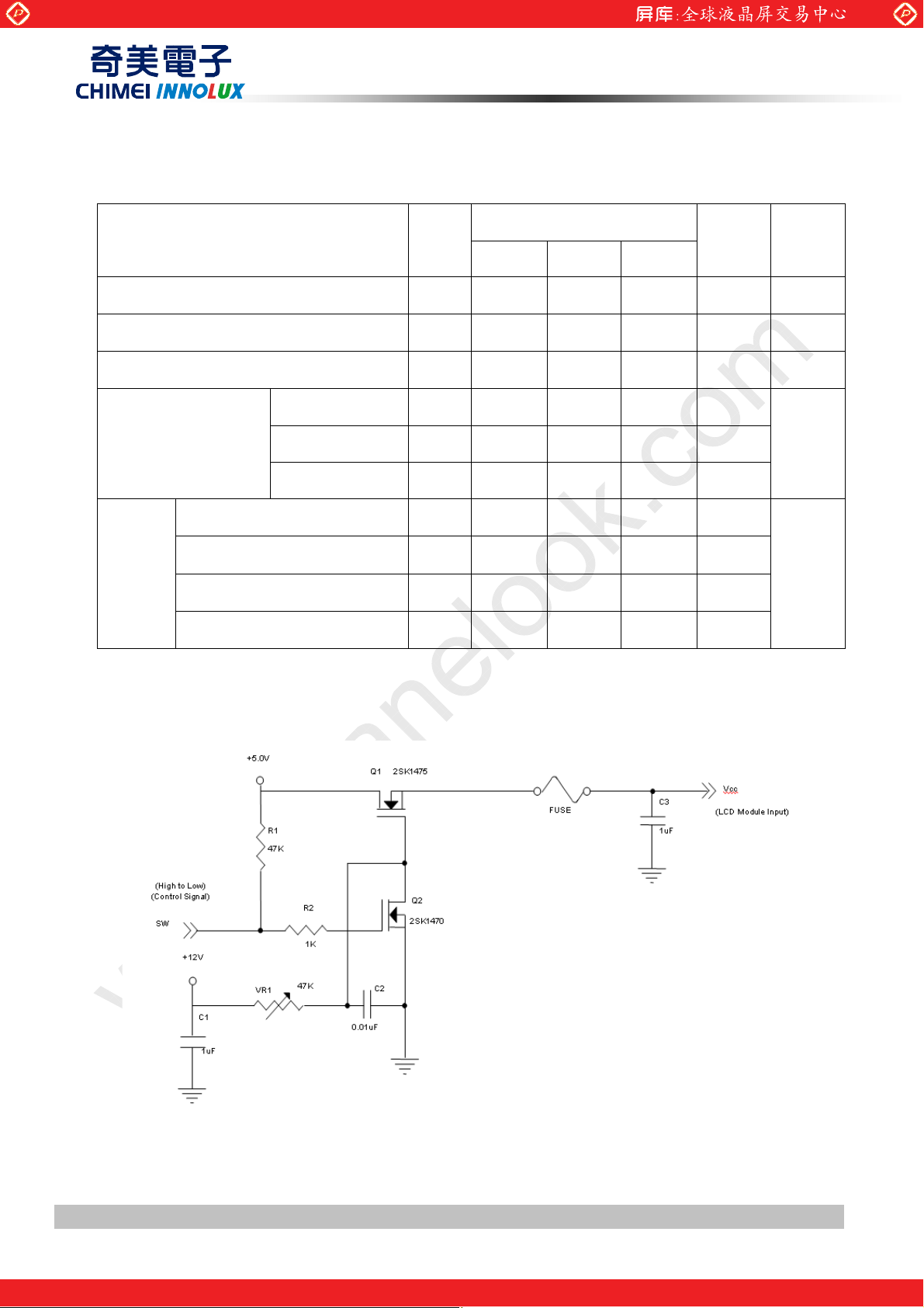
6.2 POWER ON/OFF SEQUENCE
(Ta = 25 ± 2 ºC)
To prevent a latch-up or DC operation of LCD module, the power on/off sequence should be as the
diagram below.
Timing Specifications:
Parameters
T1 0.5 -- 10 ms
T2 0 -- 50 ms
T3 450 -- -- ms
T4 90 -- -- ms
T5 0 -- 50 ms
T6 0.5 -- 100 ms
T7 500 -- -- ms
Note (1) The supply voltage of the external system for the module input should be the same as the definition
of Vcc.
Note (2) When the backlight turns on before the LCD operation of the LCD turns off, the display may
momentarily become abnormal screen.
Note (3) In case of VCC = off level, please keep the level of input signals on the low or keep a high
impedance.
Min Typ. Max
Values
Units
Note (4) T7 should be measured after the module has been fully discharged between power off and on
period.
Note (5) Interface signal shall not be kept at high impedance when the power is on.
Note (6) CMI won’t take any responsibility for the products which are damaged by the customers not
following the Power Sequence.
Note (7) There might be slight electronic noise when LCD is turned off (even backlight unit is also off). To
avoid this symptom, we suggest "Vcc falling timing" to follow "T6 spec".
Version 2.0 22 Date
The copyright belongs to CHIMEI InnoLux. Any unauthorized use is prohibited
One step solution for LCD / PDP / OLED panel application: Datasheet, inventory and accessory!
ΚΚΚΚ
03 Jun 2011
www.panelook.com
Page 23

Global LCD Panel Exchange Center
7. OPTICAL CHARACTERISTICS
7.1 TEST CONDITIONS
Item Symbol Value Unit
www.panelook.com
PRODUCT SPECIFICATION
Ambient Temperature Ta
Ambient Humidity Ha
V
Supply Voltage
Input Signal
Lamp Current
Oscillating Frequency (Inverter)
Inverter Logah F236H1-2UA-L001
The LCD module should be stabilized at given temperature for 1 hour to avoid abrupt temperature change during
measuring in a windless room.
According to typical value in "3. ELECTRICAL CHARACTERISTICS"
CC
12.5±0.5 mA
I
L
F
58±3 KHz
L
25
50
±
5
±
10
2
o
C
%RH
V
Version 2.0 23 Date
The copyright belongs to CHIMEI InnoLux. Any unauthorized use is prohibited
One step solution for LCD / PDP / OLED panel application: Datasheet, inventory and accessory!
ΚΚΚΚ
03 Jun 2011
www.panelook.com
Page 24

Global LCD Panel Exchange Center
www.panelook.com
PRODUCT SPECIFICATION
7.2 OPTICAL SPECIFICATIONS
The relative measurement methods of optical characteristics are shown in 7.2. The following items should be
measured under the test conditions described in 7.1 and stable environment shown in 7.1.
Item Symbol Condition Min. Typ. Max. Unit Note
Contrast Ratio CR 600 800 - - (2)
TR - 1.5 2.5 ms
Response Time
T
- 3.5 7 ms
F
Center Luminance of White LC 240 300 - cd/m
2
(3)
(4)
White Variation
δ
W
- - 1.33 - (6)
Cross Talk CT - - 4 % (5)
Rx 0.642 -
Red
Ry 0.331 -
θ
x=0°, θy =0°
Viewing angle
at normal direction
Gx 0.265 -
Green
Color
Chromaticity
Gy 0.602 -
Bx 0.150 -
Blue
Typ.
-0.03
Typ.
+0.03
-
By 0.063 -
Wx 0.280 -
White
Viewing Angle
Wy
Color Gamut C.G
Horizontal
Vertical
Horizontal
Vertical
θ
θ
θ
θ
+ +
x
++
Y
+ +
x
++
Y
θ
-
x
θ
-
Y
θ
-
x
θ
-
Y
CR 10
Њ
USB2000
CR
Њ
5
USB2000
150 170
140 160 -
160 178 -
150 170 -
0.290
-
- 72 - % NTSC
Deg. (1)
Version 2.0 24 Date
The copyright belongs to CHIMEI InnoLux. Any unauthorized use is prohibited
One step solution for LCD / PDP / OLED panel application: Datasheet, inventory and accessory!
ΚΚΚΚ
03 Jun 2011
www.panelook.com
Page 25

Global LCD Panel Exchange Center
Note (1) Definition of Viewing Angle (θx, θy) :
Viewing angles are measured by Autronic Conoscope Cono-80
www.panelook.com
PRODUCT SPECIFICATION
Normal
θ
x =θy = 0º
θ
x- = 90º
6 o’clock
θ
y- = 90º
y-
Note (2) Definition of Contrast Ratio (CR) :
The contrast ratio can be calculated by the following expression.
Contrast Ratio (CR) =
L255: Luminance of gray level 255
L 0: Luminance of gray level 0
x-
θy-
θx−
θ
y
θx+
+
12 o’clock direction
θ
y + = 90º
x
+
θ
x+ = 90º
L255 of Luminance Surface
L0 of Luminance Surface
CR =CR (5), where CR (X) is corresponding to the Contrast Ratio of the point X at the figure in Note (6).
Note (3) Definition of Response Time (T
100%
90%
Gray Level 255
Optical
Respons e
10%
0%
T
R
66.67ms
, TF):
R
Gray Level 0
Gray Level 255
Time
T
F
66.67ms
Version 2.0 25 Date
The copyright belongs to CHIMEI InnoLux. Any unauthorized use is prohibited
One step solution for LCD / PDP / OLED panel application: Datasheet, inventory and accessory!
ΚΚΚΚ
03 Jun 2011
www.panelook.com
Page 26

Global LCD Panel Exchange Center
(
)
(
)
Note (4) Measurement Setup:
The LCD module should be stabilized at given temperature for 1 hour to avoid abrupt
temperature change during measuring. In order to stabilize the luminance, the measurement
should be executed after lighting backlight for 1 hour in a windless room.
www.panelook.com
PRODUCT SPECIFICATION
Note (5) Definition of Luminance of White (L
Measure the luminance of gray level 255 at center point and 5 points
= L (5), where L (X) is corresponding to the luminance of the point X at the figure in Note (6).
L
C
Note (6) Definition of Cross Talk (CT):
CT = | YB – YA | / YA
×
Where:
YA = Luminance of measured location without gray level 0 pattern (cd/m2)
YB = Luminance of measured location with gray level 0 pattern (cd/m2)
(0, 0)
Active Area
Y
A, U
100 (%)
(D/2,W /8)
, L
):
C
AVE
0, 0
Active Area
Y
(D/2,W /8)
B, U
Y
(D/8,W/2)
A, L
Gray 128
Y
(7D/8,W/2)
A, R
Y
(D/8,W/2)
B, L
Gray 0
Y
(D/2,7W/8)
A, D
(D, W)
Y
(D/2,7W/8)
B, D
Version 2.0 26 Date
The copyright belongs to CHIMEI InnoLux. Any unauthorized use is prohibited
One step solution for LCD / PDP / OLED panel application: Datasheet, inventory and accessory!
(7D/8,W/2)
Y
B, R
D, W
ΚΚΚΚ
03 Jun 2011
www.panelook.com
Page 27

Global LCD Panel Exchange Center
Note (7) Definition of White Variation (δW):
Measure the luminance of gray level 255 at 5 points
δ
W = Maximum [L (1), L (2), L (3), L (4), L (5)] / Minimum [L (1), L (2), L (3), L (4), L (5)]
www.panelook.com
PRODUCT SPECIFICATION
Horizontal Line
W
W/4
W/2
Vertical Line
D/4 D/2 3D/4
1 2
3 4
D
5
Active Area
: Test Point
X=1 to 5
Version 2.0 27 Date
The copyright belongs to CHIMEI InnoLux. Any unauthorized use is prohibited
One step solution for LCD / PDP / OLED panel application: Datasheet, inventory and accessory!
ΚΚΚΚ
03 Jun 2011
www.panelook.com
Page 28

Global LCD Panel Exchange Center
www.panelook.com
PRODUCT SPECIFICATION
8. PRECAUTIONS
8.1 ASSEMBLY AND HANDLING PRECAUTIONS
[ 1 ] Do not apply rough force such as bending or twisting to the module during assembly.
[ 2 ] It is recommended to assemble or to install a module into the user’s system in clean working areas. The
dust and oil may cause electrical short or worsen the polarizer.
[ 3 ] Do not apply pressure or impulse to the module to prevent the damage of LCD panel and Backlight.
[ 4 ] Always follow the correct power-on sequence when the LCD module is turned on. This can prevent the
damage and latch-up of the CMIS LSI chips.
[ 5 ] Bezel of Set can not press or touch the panel surface. It will make light leakage or scrape.
[ 6 ] Do not plug in or pull out the I/F connector while the module is in operation.
[ 7 ] Do not disassemble the module.
[ 8 ] Use a soft dry cloth without chemicals for cleaning, because the surface of polarizer is very soft and easily
scratched.
[ 9 ] Moisture can easily penetrate into LCD module and may cause the damage during operation.
[ 10 ] When storing modules as spares for a long time, the following precaution is necessary.
[ 10.1 ] Do not leave the module in high temperature, and high humidity for a long time. It is highly
к
recommended to store the module with temperature from 0 to 35
condensation.
[ 10.2 ] The module shall be stored in dark place. Do not store the TFT-LCD module in direct sunlight or
fluorescent light.
[ 11 ] When ambient temperature is lower than 10ºC, the display quality might be reduced. For example, the
response time will become slow, and the starting voltage of CCFL will be higher than that of room
temperature.
at normal humidity without
8.2 SAFETY PRECAUTIONS
[ 1 ] The startup voltage of a Backlight is approximately 1000 Volts. It may cause an electrical shock while
assembling with the inverter. Do not disassemble the module or insert anything into the Backlight unit.
[ 2 ] If the liquid crystal material leaks from the panel, it should be kept away from the eyes or mouth. In case of
contact with hands, skin or clothes, it has to be washed away thoroughly with soap.
[ 3 ] After the module’s end of life, it is not harmful in case of normal operation and storage.
8.3 SAFETY STANDARDS
Requirement Standard remark
UL
cUL/CSA
CB
UL60950-1:2006 or Ed.2:2007
UL60065 Ed.7:2007
CAN/CSA C22.2 No.60950-1-03 or 60950-1-07
CAN/CSA C22.2 No.60065-03:2006 + A1:2006
IEC60950-1:2005 / EN60950-1:2006+ A11:2009
IEC60065:2001+ A1:2005 / EN60065:2002 + A1:2006 + A11:2008
Version 2.0 28 Date
The copyright belongs to CHIMEI InnoLux. Any unauthorized use is prohibited
One step solution for LCD / PDP / OLED panel application: Datasheet, inventory and accessory!
ΚΚΚΚ
03 Jun 2011
www.panelook.com
Page 29

Global LCD Panel Exchange Center
9. DEFINITION OF LABELS
9.1 CMI MODULE LABEL
The barcode nameplate is pasted on each module as illustration, and its definitions are as following explanation.
www.panelook.com
PRODUCT SPECIFICATION
V236H1-L03 Rev. XX
E207943
MADE IN TA IWAN
GEMN
RoHS
Model Name: V236H1-L03
Revision: Rev. XX, for example: A0, A1… B1, B2… or C1, C2…etc.
Serial ID: X X X X X X X Y M D L N N N N
V236H1-L03 Rev. XX
Serial No.
Product Line
Year, Month, Date
CMI Internal Use
CMI Internal Use
Revision
MADE IN CHINA
LEOO(or CAPG or CANO)
RoHS
Serial ID includes the information as below:
Manufactured Date:
Year : 2001=1, 2002=2, 2003=3, 2004=4…2010=0, 2011=1, 2012=2…
Month: 1~9, A~C, for Jan. ~ Dec.
Day: 1~9, A~Y, for 1st to 31st, exclude I ,O, and U.
Revision Code : Cover all the change
Serial No. : Manufacturing sequence of product
→
Product Line : 1
Line1, 2 → Line 2, …etc.
CMI Internal Use
Version 2.0 29 Date
The copyright belongs to CHIMEI InnoLux. Any unauthorized use is prohibited
One step solution for LCD / PDP / OLED panel application: Datasheet, inventory and accessory!
ΚΚΚΚ
03 Jun 2011
www.panelook.com
Page 30

Global LCD Panel Exchange Center
10. PACKAGING
10.1 PACKAGING SPECIFICATIONS
(1) 4 LCD TV modules / 1 Box
(2) Box dimensions : 620(L) X 342 (W) X 390 (H) mm
(3) Weight : Approx. 12.1 Kg (4 modules per box)
10.2 PACKAGING METHOD
(1) Carton Packing should have no failure in the following reliability test items.
Test Item Test Conditions Note
ISTA STANDARD
Random, Frequency Range: 1 – 200 Hz
Vibration
Dropping Test 1 Corner, 3 Edge, 6 Face, 61cm Non Operation
Top & Bottom: 30 minutes (+Z), 10 min (-Z),
Right & Left: 10 minutes (X)
Back & Forth 10 minutes (Y)
www.panelook.com
PRODUCT SPECIFICATION
Non Operation
Figures 10-1 and 10-2 are the packing method
Figure 10-1 packing method
Version 2.0 30 Date
The copyright belongs to CHIMEI InnoLux. Any unauthorized use is prohibited
One step solution for LCD / PDP / OLED panel application: Datasheet, inventory and accessory!
ΚΚΚΚ
03 Jun 2011
www.panelook.com
Page 31

Global LCD Panel Exchange Center
www.panelook.com
PRODUCT SPECIFICATION
Figure 10-2 packing method
Version 2.0 31 Date
The copyright belongs to CHIMEI InnoLux. Any unauthorized use is prohibited
One step solution for LCD / PDP / OLED panel application: Datasheet, inventory and accessory!
ΚΚΚΚ
03 Jun 2011
www.panelook.com
Page 32

Global LCD Panel Exchange Center
11. MECHANICAL CHARACTERISTIC
www.panelook.com
PRODUCT SPECIFICATION
Version 2.0 32 Date
The copyright belongs to CHIMEI InnoLux. Any unauthorized use is prohibited
One step solution for LCD / PDP / OLED panel application: Datasheet, inventory and accessory!
ΚΚΚΚ
03 Jun 2011
www.panelook.com
Page 33

Global LCD Panel Exchange Center
www.panelook.com
PRODUCT SPECIFICATION
Version 2.0 33 Date
The copyright belongs to CHIMEI InnoLux. Any unauthorized use is prohibited
One step solution for LCD / PDP / OLED panel application: Datasheet, inventory and accessory!
ΚΚΚΚ
03 Jun 2011
www.panelook.com
Page 34

Global LCD Panel Exchange Center
www.panelook.com
PRODUCT SPECIFICATION
Version 2.0 34 Date
The copyright belongs to CHIMEI InnoLux. Any unauthorized use is prohibited
One step solution for LCD / PDP / OLED panel application: Datasheet, inventory and accessory!
ΚΚΚΚ
03 Jun 2011
www.panelook.com
 Loading...