

Page 1
Customer:
PRODUCT SPECIFICATION
□ Tentative Specification
□ Preliminary Specification
■ Approval Specification
MODEL NO.: V236BJ1
SUFFIX: P01
APPROVED BY SIGNATURE
Name / Title
Note
Please return 1 copy for your confirmation with your signature and
comments.
Approved By Checked By Prepared By
Chao-Chun Chung
YP Lee
Chris Chen
Version 2.1
1
The copyright belongs to CHIMEI InnoLux. Any unauthorized use is prohibited
Date
12 Sep. 2012
Page 2

PRODUCT SPECIFICATION
CONTENTS
1. GENERAL DESCRIPTION......................................................................................................................................4
1.1 OVERVIEW .....................................................................................................................................................4
1.2 FEATURES ..................................................................................................................................................... 4
1.3 MECHANICAL SPECIFICATIONS ...................................................................................................................4
2. ABSOLUTE MAXIMUM RATINGS...........................................................................................................................5
2.1 ABSOLUTE RATINGS OF ENVIRONMENT.....................................................................................................5
2.2 PACKAGE STORAGE .....................................................................................................................................6
2.3 ELECTRICAL ABSOLUTE RATINGS (OPEN CELL)........................................................................................ 6
3. ELECTRICAL CHARACTERISTICS........................................................................................................................ 7
3.1 TFT LCD MODULE.......................................................................................................................................... 7
4. BLOCK DIAGRAM OF INTERFACE........................................................................................................................9
4.1 TFT LCD MODULE.......................................................................................................................................... 9
5. INPUT TERMINAL PIN ASSIGNMENT..................................................................................................................10
5.1 TFT LCD MODULE INPUT ............................................................................................................................ 10
5.2 COLOR DATA INPUT ASSIGNMENT.............................................................................................................12
5.3 FLICKER (Vcom) ADJUSTMENT................................................................................................................... 13
6. INTERFACE TIMING ............................................................................................................................................14
6.1 INPUT SIGNAL TIMING SPECIFICATIONS................................................................................................... 14
6.2 POWER ON/OFF SEQUENCE......................................................................................................................16
7. OPTICAL CHARACTERISTICS ............................................................................................................................ 17
7.1 TEST CONDITIONS ...................................................................................................................................... 17
7.2 OPTICAL SPECIFICATIONS ......................................................................................................................... 18
8. DEFINITION OF LABELS ..................................................................................................................................... 21
8.1 OPEN CELL LABEL....................................................................................................................................... 21
8.2 CARTON LABEL ...........................................................................................................................................21
9. PACKAGING......................................................................................................................................................... 22
9.1 PACKING SPECIFICATIONS.........................................................................................................................22
9.2 PACKING METHOD......................................................................................................................................22
10. PRECAUTIONS.................................................................................................................................................. 24
10.1 ASSEMBLY AND HANDLING PRECAUTIONS............................................................................................. 24
10.2 SAFETY PRECAUTIONS ............................................................................................................................ 24
11. MECHANICAL CHARACTERISTIC..................................................................................................................... 25
Version 2.1
2
The copyright belongs to CHIMEI InnoLux. Any unauthorized use is prohibited
Date
12 Sep. 2012
Page 3
Version
Ver. 2.1 Sep.12, 2012
Date
Page
(New)
All
PRODUCT SPECIFICATION
REVISION HISTORY
Section Description
All The Approval Specification for 0.5mm Cell was first issued.
Version 2.1
3
The copyright belongs to CHIMEI InnoLux. Any unauthorized use is prohibited
Date
12 Sep. 2012
Page 4
The mounting inclination of the connector makes the
PRODUCT SPECIFICATION
1. GENERAL DESCRIPTION
1.1 OVERVIEW
V236BJ1-P01 is a 23.6” TFT Liquid Crystal Display product with driver ICs and 1ch-LVDS interface. This product
supports 1366*768 HDTV format and can display 16.7M colors (8-bit / color).
1.2 FEATURES
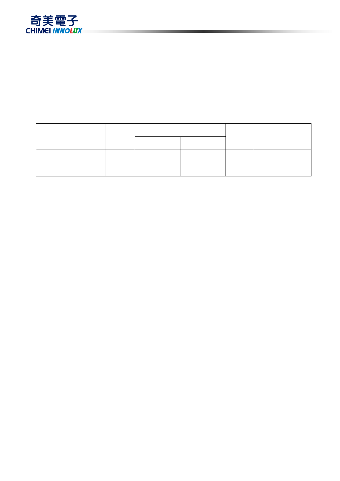
CHARACTERISTICS ITEMS SPECIFICATIONS
Screen Diagonal [in] 23.6
Pixels [lines] 1366 x 768
Active Area [mm] 521.4705 (H) x 293.184 (V)
Sub-Pixel Pitch [mm] 0.12725 (H) x 0.38175 (V)
Pixel Arrangement RGB vertical stripe
Weight [g] TYP. 500 g
Physical Size [mm] 535.06(W) × 307.34(H) × 1.53(D) Typ.
Display Mode Transmissive mode / Normallly black
Contrast Ratio
Glass thickness (Array / CF) [mm] 0.5 / 0.5
Viewing Angle (CR>20)
Color Chromaticity * Please refer to “color chromaticity” on p.22
Cell Transparency [%] 5.5%
Polarizer Surface Treatment Anti-Glare coating (Haze 1%),Hard coating (3H)
3000:1 Typ.
(Typical value measure at CMI’s module)
+88/-88(H), +88/-88(V) Typ. (CR 20)
(Typical value measure at CMI’s module)
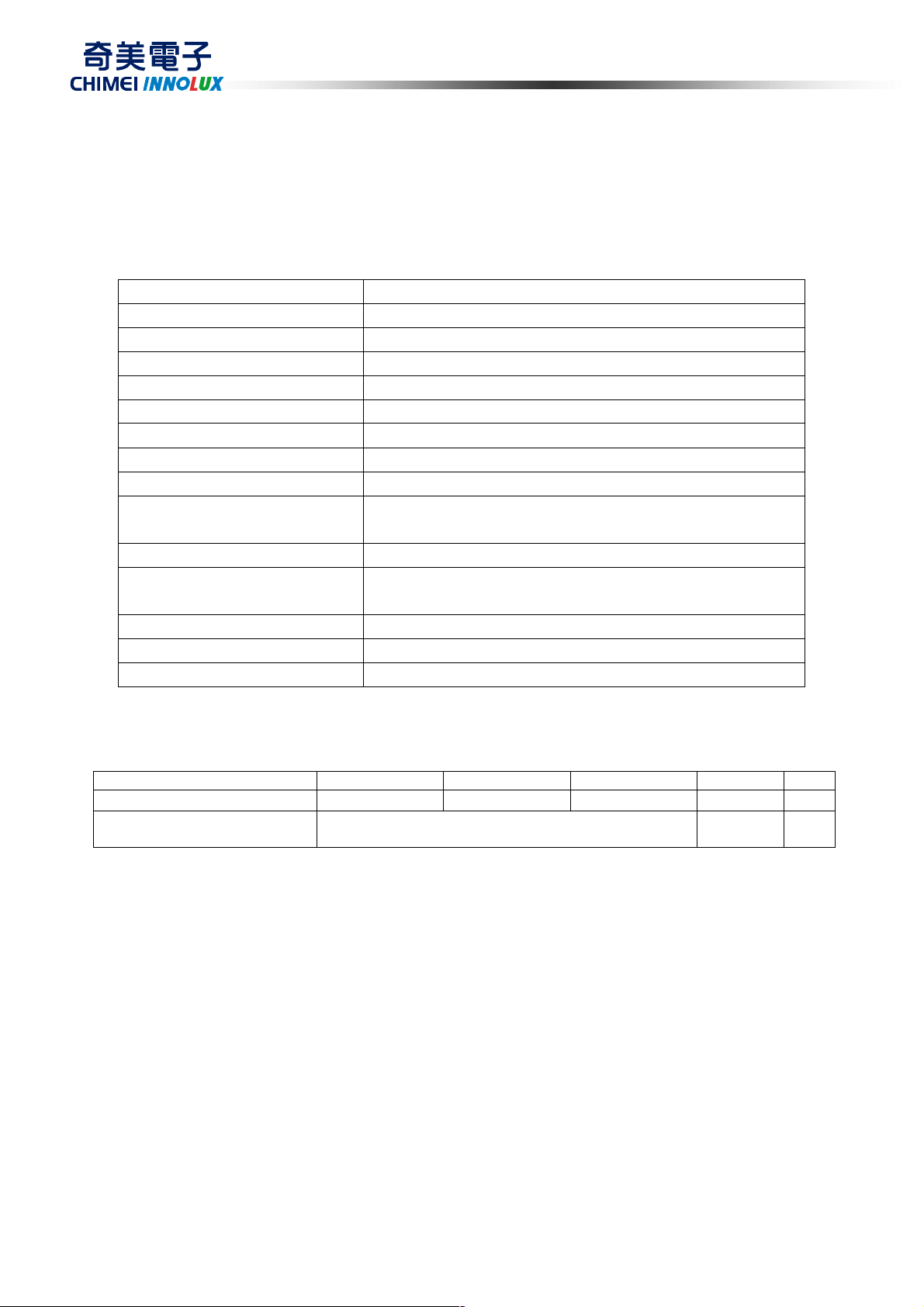
1.3 MECHANICAL SPECIFICATIONS
Item Min. Typ. Max. Unit Note
Weight 485 500 515 g -
I/F connector mounting position
Note (1) Please refer to the attached drawings for more information of front and back outline dimensions.
Note (2) Connector mounting position
screen center within ± 0.5mm as the horizontal.
(2)
Version 2.1
4
The copyright belongs to CHIMEI InnoLux. Any unauthorized use is prohibited
Date
12 Sep. 2012
Page 5
40 60 20
PRODUCT SPECIFICATION
2. ABSOLUTE MAXIMUM RATINGS
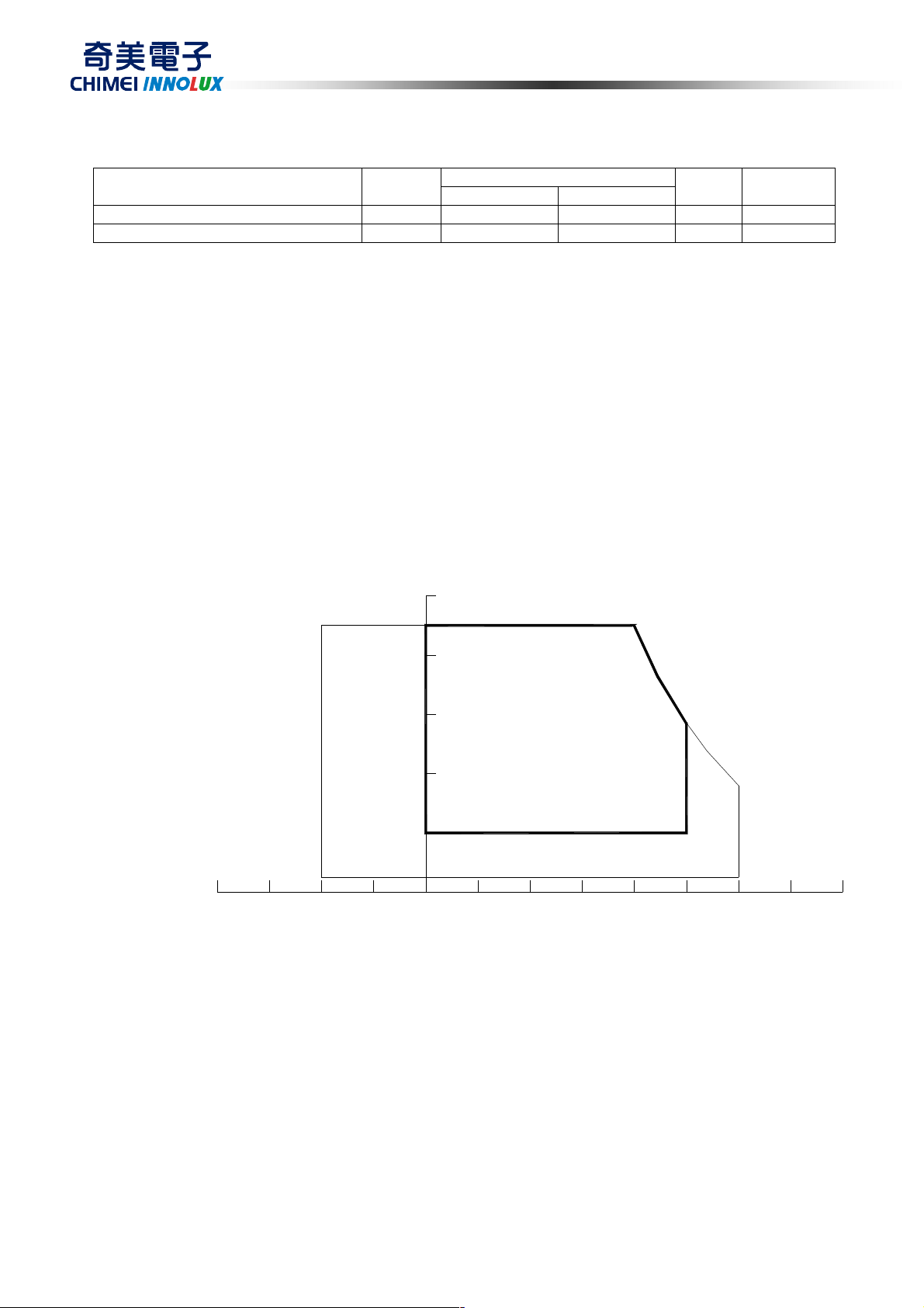
2.1 ABSOLUTE RATINGS OF ENVIRONMENT
Item Symbol
Storage Temperature TST -20 +60 ºC (1)
Operating Ambient Temperature TOP 0 50 ºC (1), (2)
Note (1) Temperature and relative humidity range is shown in the figure below.
(a) 90 %RH Max. (Ta 40 ºC).
(b) Wet-bulb temperature should be 39 ºC Max. (Ta > 40 ºC).
(c) No condensation.
Note (2) The maximum operating temperature is based on the test condition that the surface temperature of
display area is less than or equal to 65 ºC with LCD module alone in a temperature controlled chamber.
Thermal management should be considered in final product design to prevent the surface temperature
of display area from being over 65 ºC. The range of operating temperature may degrade in case of
improper thermal management in final product design.
Min. Max.
Value
Unit Note
Relative Humidity (%RH)
100
90
80
Operating Range
10
Storage Range
Temperature (ºC)
80 60 -20 40 0 20 -40
Version 2.1
5
The copyright belongs to CHIMEI InnoLux. Any unauthorized use is prohibited
Date
12 Sep. 2012
Page 6
PRODUCT SPECIFICATION
2.2 PACKAGE STORAGE
When storing modules as spares for a long time, the following precaution is necessary.
(a) Do not leave the module in high temperature, and high humidity for a long time, It is highly recommended to
store the module with temperature from 0 to 35 at normal humidity without condensation.
(b) The module shall be stored in dark place. Do not store the TFT-LCD module in direct sunlight or fluorescent
light.
2.3 ELECTRICAL ABSOLUTE RATINGS
Item Symbol
Power Supply Voltage VCC -0.3 13.5 V
Logic Input Voltage VIN -0.3 3.6 V
Note (1) Permanent damage to the device may occur if maximum values are exceeded. Function operation
should be restricted to the conditions described under Normal Operating Conditions.
(OPEN CELL)
Value
Min. Max.
Unit Note
(1)
Version 2.1
6
The copyright belongs to CHIMEI InnoLux. Any unauthorized use is prohibited
Date
12 Sep. 2012
Page 7
PRODUCT SPECIFICATION
3. ELECTRICAL CHARACTERISTICS
3.1 TFT LCD MODULE
(Ta = 25 ± 2 ºC)
Value
Parameter Symbol
Unit Note
Min. Typ. Max.
Power Supply Voltage VCC 10.8 12 13.2 V (1)
Rush Current I
White Pattern PT
Power
consumption
Black Pattern PT
Heavy Loading pattern
Ex: Horizontal Stripe
(by cell and platform)
White Pattern PT
Power Supply
Current
Black Pattern PT
Heavy Loading pattern
Ex: Horizontal Stripe
(by cell and platform)
Differential Input High
Threshold Voltage
Differential Input Low
Threshold Voltage
LVDS interface
Common Input Voltage VCM 1.0 1.2 1.4 V
Differential input voltage
(single-end)
Terminating Resistor RT
RUSH
PT
PT
V
LVTH
V
LVTL
| 200
|V
ID
5.0976 6.053
+100
-300
3.172 A (2)
5.256 6.24
3.269 3.822
0.44 0.52
0.272 0.3185
0.425 0.5044
100
+300 mV
-100 mV
600 mV
W
(3)
A
(4)
ohm
CMOS
interface
Input High Threshold
Voltage
Input Low Threshold
Voltage
2.7
V
IH
V
0
IL
Note (1) The module should be always operated within the above ranges.
The ripple voltage should be controlled under 10% of Vcc (Typ.).
Note (2) Measurement condition :
GND
Version 2.1
7
The copyright belongs to CHIMEI InnoLux. Any unauthorized use is prohibited
3.3 V
0.7 V
Vcc rising time is 470us
0.9Vcc
0.1Vcc
470us
Date
12 Sep. 2012
Vcc
Page 8
PRODUCT SPECIFICATION
Note (3) The specified power supply current is under the conditions at Vcc = 12 V, Ta = 25 ± 2 ºC, fv = 60 Hz,
whereas a power dissipation check pattern below is displayed.
a. White Pattern
Active Area
b. Black Pattern
Active Area
c. Heavy Loading pattern Ex: Horizontal Stripe
Note (4) The LVDS input characteristics is shown as below :
Version 2.1
8
The copyright belongs to CHIMEI InnoLux. Any unauthorized use is prohibited
Date
12 Sep. 2012
Page 9

X+C Board
P-TWO=187053
-
30091 or
F
OXCONN=GS23302
-
1321S
-7H
GND
SDA SCL
4. BLOCK DIAGRAM OF INTERFACE
4.1 TFT LCD MODULE
PRODUCT SPECIFICATION
Vcc
TFT LCD PANEL
(1366x3x768)
INPUT CONNECTOR,
SELLVDS
RX0(+/-)
RX1(+/-)
RX2(+/-)
RX3(+/-)
CLK(+/-)
Version 2.1
9
The copyright belongs to CHIMEI InnoLux. Any unauthorized use is prohibited
Date
12 Sep. 2012
Page 10

PRODUCT SPECIFICATION
5. INPUT TERMINAL PIN ASSIGNMENT
5.1 TFT LCD MODULE INPUT
CNF1 Connector Pin Assignment P-TWO=187053-30091 or FOXCONN=GS23302-1321S-7H
Pin Name Description Remark
1 VCC +12.0V power supply
2 VCC +12.0V power supply
3 VCC +12.0V power supply
4 VCC +12.0V power supply
5 GND Ground
6 GND Ground
7 GND Ground
8 NC
9 SELLVDS Select LVDS Format (3)(4)
10 NC NC (2)
11 GND Ground
12 RX0- Negative LVDS differential data input. Channel 0
13 RX0+ Positive LVDS differential data input. Channel 0
14 GND Ground
15 RX1- Negative LVDS differential data input. Channel 1
16 RX1+ Positive LVDS differential data input. Channel 1
17 GND Ground
18 RX2- Negative LVDS differential data input. Channel 2
19 RX2+ Positive LVDS differential data input. Channel 2
20 GND Ground
21 RXLCK- Negative LVDS differential clock input.
22 RXCLK+ Positive LVDS differential clock input.
23 GND Ground
24 RX3- Negative LVDS differential data input. Channel 3
25 RX3+ Positive LVDS differential data input. Channel 3
26 GND Ground
27 NC No connection (2)
28 SCL I2C clock (For Vcom tunning)
29
SDA I2C data (For Vcom tunning)
No connection
(2)
30 GND Ground
Note (1) Connector type: (P-TWO=187053-30091 or FOXCONN=GS23302-1321S-7H )
LVDS connector pin orderdefined as follows
Version 2.1
10
The copyright belongs to CHIMEI InnoLux. Any unauthorized use is prohibited
Date
12 Sep. 2012
Page 11

PRODUCT SPECIFICATION
Note (2) Reserved for internal use. Please leave it open.
Note (3) LVDS data format Selection (0V~0.7V→VESA , 2.7V~3.3V/Open→JEDIA)
SELLVDS Mode
0V~0.7V VESA
2.7V~3.3V/Open
L : Connect to GND, H : Connect to +3.3V
Note (4) Interface optional pin has internal scheme as following diagram. Customer should keep the interface
voltage levelrequirement which including Panel board loading as below.
JEIDA
3.3V
System Board
Panel Board
Interface Voltage Level
VH > V
VL < V
Note (5) LVDS connector mating dimension range request is 0.93mm~1.0mm as below.
Note (6) The screw hole which is distant from the connector is merged with Ground.
IH
IL
Version 2.1
11
The copyright belongs to CHIMEI InnoLux. Any unauthorized use is prohibited
Date
12 Sep. 2012
Page 12

1 0 0 0 1 1 1 0 1 0 0 0 1 1 1 0 1 0 0 0 1 1 1 0 1 0 0 0 1 1 1 0 1 0 0 0 1 1 1 0 1 0 0 0 1 1 1 0 1 0 0 0 1 1 1 0 1 0 0 0 1 1 1 0 0 1 0 1 0 1 1 0 0 1 0 1 0 1 1 0 0 1 0 1 0 1 1 0 0 1 0 1 0 1 1 0 0 1 0 1 0 1 1 0 0 1 0 1 0 1 1 0 0 1 0 1 0 1 1 0 0 1 0 1 0 1 1 0 0 0 1 1 1 0 1 0 0 0 1 1 1 0 1 0 0 0 1 1 1 0 1 0 0 0 1 1 1 0 1 0 0 0 1 1 1 0 1 0 0 0 1 1 1 0 1 0 0 0 1 1 1 0 1 0 0 0 1 1 1 0 1
0 0 : : 1 1 1 0 0 0 : : 1 1 1 0 0 0 : : 1 1 1 0 0 0 : : 1 1 1 0 0 0 : : 1 1 1 0 0 0 : : 1 1 1 0 0 1 : : 0 1 1 0 1 0 : : 1 0 1 0 0 0 : : 0 0 0 0 0 0 : : 0 0 0 0 0 0 : : 0 0 0 0 0 0 : : 0 0 0 0 0 0 : : 0 0 0 0 0 0 : : 0 0 0 0 0 0 : : 0 0 0 0 0 0 : : 0 0 0 0 0 0 : : 0 0 0 0 0 0 : : 0 0 0 0 0 0 : : 0 0 0 0 0 0 : : 0 0 0 0 0 0 : : 0 0 0 0 0 0 : : 0 0 0 0 0 0 : : 0 0 0 0 0 0 : : 0 0 0
0 0 : : 0 0 0 0 0 0 : : 0 0 0 0 0 0 : : 0 0 0 0 0 0 : : 0 0 0 0 0 0 : : 0 0 0 0 0 0 : : 0 0 0 0 0 0 : : 0 0 0 0 0 0 : : 0 0 0 0 0 0 : : 1 1 1 0 0 0 : : 1 1 1 0 0 0 : : 1 1 1 0 0 0 : : 1 1 1 0 0 0 : : 1 1 1 0 0 0 : : 1 1 1 0 0 1 : : 0 1 1 0 1 0 : : 1 0 1 0 0 0 : : 0 0 0 0 0 0 : : 0 0 0 0 0 0 : : 0 0 0 0 0 0 : : 0 0 0 0 0 0 : : 0 0 0 0 0 0 : : 0 0 0 0 0 0 : : 0 0 0 0 0 0 : : 0 0 0
0 0 : : 0 0 0 0 0 0 : : 0 0 0 0 0 0 : : 0 0 0 0 0 0 : : 0 0 0 0 0 0 : : 0 0 0 0 0 0 : : 0 0 0 0 0 0 : : 0 0 0 0 0 0 : : 0 0 0 0 0 0 : : 0 0 0 0 0 0 : : 0 0 0 0 0 0 : : 0 0 0 0 0 0 : : 0 0 0 0 0 0 : : 0 0 0 0 0 0 : : 0 0 0 0 0 0 : : 0 0 0 0 0 0 : : 0 0 0 0 0 0 : : 1 1 1 0 0 0 : : 1 1 1 0 0 0 : : 1 1 1 0 0 0 : : 1 1 1 0 0 0 : : 1 1 1 0 0 0 : : 1 1 1 0 0 1 : : 0 1 1 0 1 0 : : 1 0 1
PRODUCT SPECIFICATION
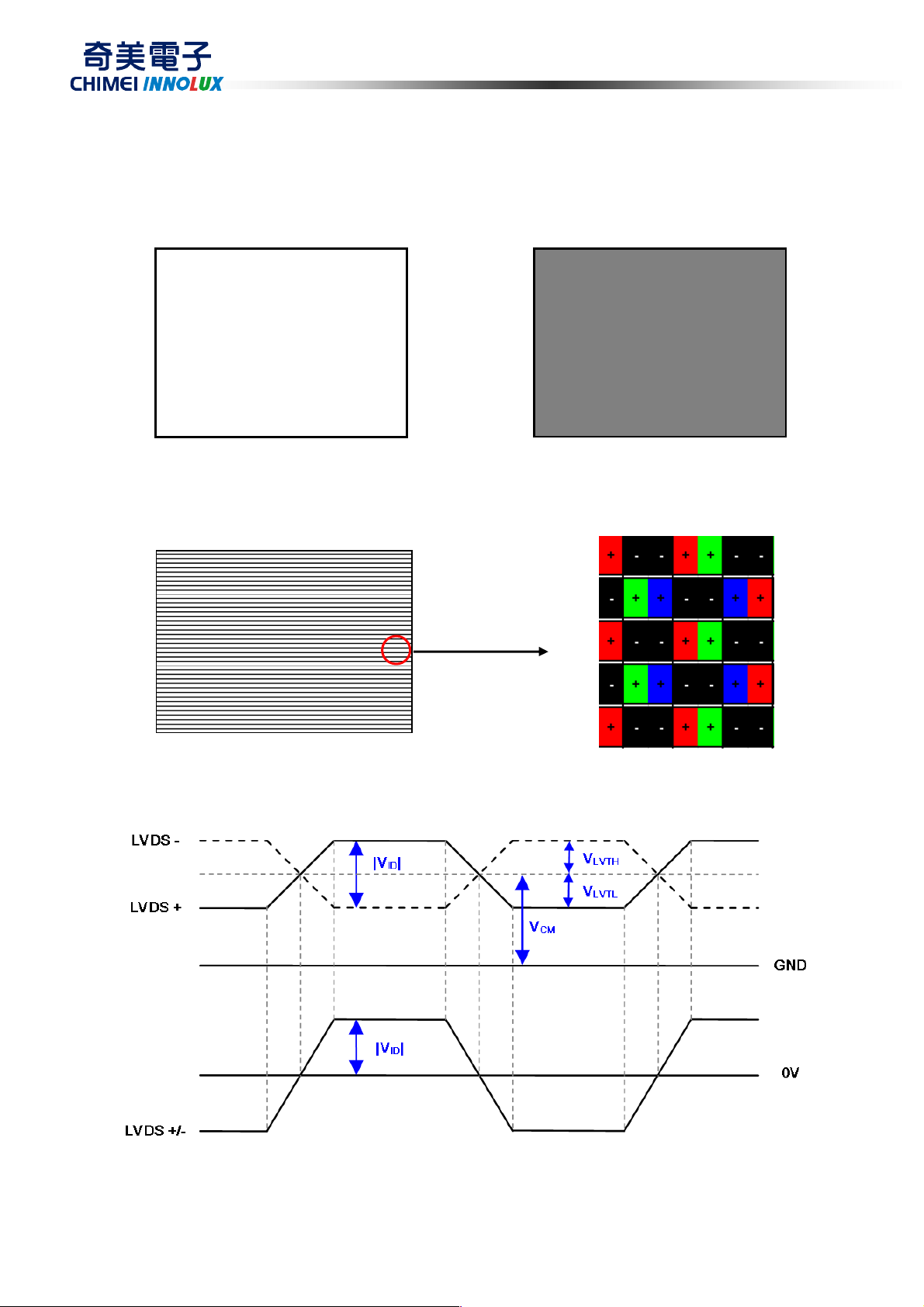
5.2 COLOR DATA INPUT ASSIGNMENT
The brightness of each primary color (red, green and blue) is based on the 8-bit gray scale data input for the
color. The higher the binary input, the brighter the color. The table below provides the assignment of the color
versus data input.
Data Signal
Color
R7 R6 R5 R4 R3 R2 R1 R0 G7 G6 G5 G4 G3 G2 G1 G0 B7 B6 B5 B4 B3 B2 B1 B0
Black
Red
Green
Basic
Colors
Gray
Scale
Of
Red
Gray
Scale
Of
Green
Gray
Scale
Of
Blue
Note (1) 0: Low Level Voltage, 1: High Level Voltage
Blue
Cyan
Magenta
Yellow
White
Red (0) / Dark
Red (1)
Red (2)
:
:
Red (253)
Red (254)
Red (255)
Green (0) / Dark
Green (1)
Green (2)
:
:
Green (253)
Green (254)
Green (255)
Blue (0) / Dark
Blue (1)
Blue (2)
:
:
Blue (253)
Blue (254)
Blue (255)
0
0
0
0
Red Green Blue
Version 2.1
12
The copyright belongs to CHIMEI InnoLux. Any unauthorized use is prohibited
Date
12 Sep. 2012
Page 13

PRODUCT SPECIFICATION
5.3 FLICKER (Vcom) ADJUSTMENT
(1) Adjustment Pattern :
The adjustment pattern is shown as below. If customer needs below pattern, please directly contact with
CMI account FAE.
(2) Adjustment method: (Digital V-com)
Programmable memory IC is used for Digital V-com adjustment in this model. CMI provide Auto Vcom tools to
adjust Digital V-com.The detail connection and setting instruction, please directly contact with Account FAE or
refer CMI Auto V-com adjustment OI. Below items is suggested to be ready before Digital V-com adjustment in
customer LCM line.
a. USB Sensor Board.
b. Programmable software.
c. Document: Auto V-com adjustment suggestion OI.
Version 2.1
13
The copyright belongs to CHIMEI InnoLux. Any unauthorized use is prohibited
Date
12 Sep. 2012
Page 14

DE T
hb
Valid Display Data (
1366 clocks)
T
c
PRODUCT SPECIFICATION
6. INTERFACE TIMING
6.1 INPUT SIGNAL TIMING SPECIFICATIONS
(Ta = 25 ± 2 ºC)
The input signal timing specifications are shown as the following table and timing diagram.
Signal Item Symbol
F
clkin
(=1/TC)
T
clkin_mod
F
F
SSM
LVDS
Receiver
Clock
LVDS
Frequency
Input cycle to
cycle jitter
Spread spectrum
modulation range
Spread spectrum
modulation frequency
Setup Time Tlvsu
rcl
Min. Typ. Max. Unit Note
67.67 76 82 MHz
F
-2%
clkin
600
200 ps (2)
+2%
F
clkin
200 KHz
Receiver
Data
Hold Time Tlvhd
600
Fr5 47 50 53 Hz
Frame Rate
57 60 63 Hz
Vertical
Active
Display
Term
Total Tv 778 806 986 Th
Display Tvd 768 768 768 Th
F
r6
MHz
(3)
ps
ps
Tv=Tvd+Tvb
Blank Tvb 10 38 218 Th
Horizontal
Active
Display
Term
Total Th 1446 1560 1936 Tc
Display Thd 1366 1366 1366 Tc
Blank Thb 80 194 570 Tc
Th=Thd+Thb
Note (1) Please make sure the range of pixel clock has follow the below equation :
Fclkin(max) Fr6 Tv Th
Fr5 Tv Th Fclkin (min)
Note (2) This module is operated in DE only mode and please follow the input signal timing diagram below :
T
v
T
vd
T
vb
DCLK
Th
T
hd
Version 2.1
DE
DATA
14
The copyright belongs to CHIMEI InnoLux. Any unauthorized use is prohibited
Date
12 Sep. 2012
Page 15

PRODUCT SPECIFICATION
Note (3) The input clock cycle-to-cycle jitter is defined as below figures. Trcl = | T1 – T|
Note (4) The SSCG (Spread spectrum clock generator) is defined as below figures.
Note (5) The LVDS timing diagram and the receiver skew margin is defined and shown in following figure.
RXCLK+/-
RXn+/-
Version 2.1
T
RSKM
15
The copyright belongs to CHIMEI InnoLux. Any unauthorized use is prohibited
Date
12 Sep. 2012
Page 16

500ms
T4
0T8T3
T910ms
PRODUCT SPECIFICATION
6.2 POWER ON/OFF SEQUENCE
To prevent a latch-up or DC operation of LCD module, the power on/off sequence should be as the diagram
below.
0V
0.5 T110ms
0T2200ms
0T3
LVDS Signals
0T7T2
0V
Option Signals (SELLVDS)
Backlight (Recommended)
500msT5
100msT6
0.9Vcc
0.1VCC
Power On
T7
0.9Vcc
0.1Vcc
T3 T1
2
T
T4
Power Off
8
T
50%
50%
T5
T6
Vcc Dip
Vcc
Vcc(typ.) x 0.85
T9
0V
Note (1) The supply voltage of the external system for the module input should follow the definition of Vcc.
Note (2) Apply the lamp voltage within the LCD operation range. When the backlight turns on before the LCD
operation or the LCD turns off before the backlight turns off, the display may momentarily become
abnormal screen.
Note (3) In case of VCC is in off level, please keep the level of input signals on the low or high impedance. If
T2<0,that maybe cause electrical overstress failure.
Note (4) T4 should be measured after the module has been fully discharged between power off and on period.
Note (5) Interface signal shall not be kept at high impedance when the power is on.
Note (6) Vcc must decay smoothly when power-off.
Version 2.1
16
The copyright belongs to CHIMEI InnoLux. Any unauthorized use is prohibited
Date
12 Sep. 2012
Page 17

7. OPTICAL CHARACTERISTICS
7.1 TEST CONDITIONS
Item Symbol Value Unit
PRODUCT SPECIFICATION
Ambient Temperature Ta
Ambient Humidity Ha
Supply Voltage VCC 12V V
Input Signal According to typical value in "3. ELECTRICAL CHARACTERISTICS"
Lamp Current IL 12.5±0.5 mA
Oscillating Frequency (Inverter)
Vertical Frame Rate Fr 60 Hz
The LCD module should be stabilized at given temperature for 1 hour to avoid abrupt temperature change during
measuring in a windless room.
FW 58±3 KHz
25±2
50±10
o
C
%RH
Version 2.1
17
The copyright belongs to CHIMEI InnoLux. Any unauthorized use is prohibited
Date
12 Sep. 2012
Page 18

PRODUCT SPECIFICATION
7.2 OPTICAL SPECIFICATIONS
The relative measurement methods of optical characteristics are shown as below. The following items
should be measured under the test conditions described in 7.1 and stable environment shown in 7.1.
Item Symbol
Rcx 0.654
Red
Rcy 0.329
Gcx 0.274
Green
Color
Chromaticity
Blue
White
Center Transmittance T% - 5.5 - % (1),(6)
Transmittance Variation
Contrast Ratio CR
Response Time
Horizontal
Viewing
Angle
Vertical
Gcy 0.602
Bcx 0.133
Bcy 0.115
Wcx 0.310
Wcy
δT
Gray to
gray
θx+
θx-
θY+
θY-
Viewing Angle at Normal
Standard light source “C”
with CMI Module @60Hz
Condition Min. Typ. Max. Unit Note
θx=0°, θY =0°
Direction
θx=0°, θY =0°
=0°, θY =0°
θ
x
with CMI Module.
CR≥20 (VA Model)
with CMI Module
-0.03
+0.03
0.356
- - 1.42 - (1),(5)
2000 3000
- 8.5 20 ms
80
80
80
80
88
88
88
88
- - (1),(3)
-
-
-
-
-
-
-
-
-
-
-
-
Deg. (1),(2)
(1)
(1),(4)
Note (0) Light source is the standard light source ”C” which is defined by CIE and driving voltage are based on
suitable gamma voltages. The calculating method is as following :
1.Measure Module’s and BLU’s spectrum at center point. W, R, G, B are with signal input. BLU
(V236BJ1-L01) is supplied by CMI.
2. Calculate cell’s spectrum.
3.Calculate cell’s chromaticity by using the spectrum of standard light source “C”.
Note (1) Light source is the BLU which supplied by CMI and driving voltage are based on suitable gamma
voltages.
Version 2.1
The copyright belongs to CHIMEI InnoLux. Any unauthorized use is prohibited
18
Date
12 Sep. 2012
Page 19

Note (2) Definition of Viewing Angle (θx, θy):
0%
Time
Viewing angles are measured by Autronic Conoscope Cono-80
PRODUCT SPECIFICATION
θX- = 90º
x-
6 o’clock
θy- = 90º
y-
Note (3) Definition of Contrast Ratio (CR):
The contrast ratio can be calculated by the following expression.
Contrast Ratio (CR) =
Normal
θx = θy = 0º
θy- θy+
θx−
θx+
12 o’clock direction
y+
θy+ = 90º
x+
θX+ = 90º
L255 of Luminance Surface
L0 of Luminance Surface
L255: Luminance of gray level 255
L 0: Luminance of gray level 0
CR = CR (5), where CR (X) is corresponding to the Contrast Ratio of the point X at the figure in Note (5).
Note (4) Definition of Response Time (TR, TF):
Response
100%
90%
Optical
10%
Gray Level 255
TR
Gray Level 0
Gray Level 255
TF
Version 2.1
The copyright belongs to CHIMEI InnoLux. Any unauthorized use is prohibited
19
Date
12 Sep. 2012
Page 20

Note (5) Definition of White Variation (δW):
Measure the luminance of gray level 255 at 5 points
δW = Maximum [L (1), L (2), L (3), L (4), L (5)] / Minimum [L (1), L (2), L (3), L (4), L (5)]
PRODUCT SPECIFICATION
Horizontal Line
D/4 D/2 3D/4
W/4
1 2
W/2
W
Vertical Line
3W/4
3 4
Note (6) Definition of Transmittance (T%) :
Measure the luminance of gray level 255 at center point of LCD module.
Transmittance (T%) =
D
5
Active Area
: Test Point
X
X=1 to 5
module LCD of Luminance
unit backligh of Luminance
×
100%
Version 2.1
The copyright belongs to CHIMEI InnoLux. Any unauthorized use is prohibited
20
Date
12 Sep. 2012
Page 21

PRODUCT SPECIFICATION
V
236BJ1
-P0
1 Rev.
V
236BJ1
-P01 R
ev.
8. DEFINITION OF LABELS
8.1 OPEN CELL LABEL
The barcode nameplate is pasted on each open cell as illustration for CMI internal control.
XXXXXXXXXXXXXX
8.2 CARTON LABEL
The barcode nameplate is pasted on each box as illustration, and its definitions are as following explanation
P.O. NO.
XXXXXXXXXXXXXX
Made in Taiwan
Parts ID. Quantities 15
Model Name V236BJ1-P01 Rev.
Carton ID.
XXXXXXXXXXXXXX
P.O. NO.
Parts ID. Quantities 15
Model Name V236BJ1-P01 Rev.
Carton ID.
RoHS
Made in China
RoHS
(a) Model Name: V236BJ1– P01
(b) Carton ID: CMI internal control
(c) Quantities: 15
Version 2.1
The copyright belongs to CHIMEI InnoLux. Any unauthorized use is prohibited
XXXXXXXXXXXXXX
21
Date
12 Sep. 2012
Page 22

9. PACKAGING
9.1 PACKING SPECIFICATIONS
(1) 15 PCS LCD TV Panels / 1 Box
(2) Box dimensions : 630 (L) X 480 (W) X93 (H)mm
(3) Weight : approximately 10.3Kg
(4) 540 PCS LCD TV Panels / 1 Group
9.2 PACKING METHOD
Packing method (Hard Box) is shown in following figures.
PRODUCT SPECIFICATION
Figure.9-1 packing method
Version 2.1
The copyright belongs to CHIMEI InnoLux. Any unauthorized use is prohibited
22
Date
12 Sep. 2012
Page 23

PRODUCT SPECIFICATION
Figure.9-2 packing method
Version 2.1
The copyright belongs to CHIMEI InnoLux. Any unauthorized use is prohibited
23
Date
12 Sep. 2012
Page 24

PRODUCT SPECIFICATION
10. PRECAUTIONS
10.1 ASSEMBLY AND HANDLING PRECAUTIONS
(1) Do not apply rough force such as bending or twisting to the product during assembly.
(2) To assemble backlight or install module into user’s system can be only in clean working areas. The dust
and oil may cause electrical short or worsen the polarizer.
(3) It’s not permitted to have pressure or impulse on the module because the LCD panel will be damaged.
(4) Always follow the correct power sequence when the product is connecting and operating. This can
prevent damage to the CMOS LSI chips during latch-up.
(5) Do not pull the I/F connector in or out while the module is operating.
(6) Use a soft dry cloth without chemicals for cleaning, because the surface of polarizer is very soft and
easily scratched.
(7) It is dangerous that moisture come into or contacted the product, because moisture may damage the
product when it is operating.
(8) High temperature or humidity may reduce the performance of module. Please store this product within
the specified storage conditions.
(9) When ambient temperature is lower than 10ºC may reduce the display quality. For example, the
response time will become slowly.
10.2 SAFETY PRECAUTIONS
(1) If the liquid crystal material leaks from the panel, it should be kept away from the eyes or mouth. In case of
contact with hands, skin or clothes, it has to be washed away thoroughly with soap.
(2) After the product’s end of life, it is not harmful in case of normal operation and storage.
Version 2.1
The copyright belongs to CHIMEI InnoLux. Any unauthorized use is prohibited
24
Date
12 Sep. 2012
Page 25

11. MECHANICAL CHARACTERISTIC
PRODUCT SPECIFICATION
Version 2.1
The copyright belongs to CHIMEI InnoLux. Any unauthorized use is prohibited
25
Date
12 Sep. 2012
 Loading...