

Page 1
PRODUCT SPECIFICATION
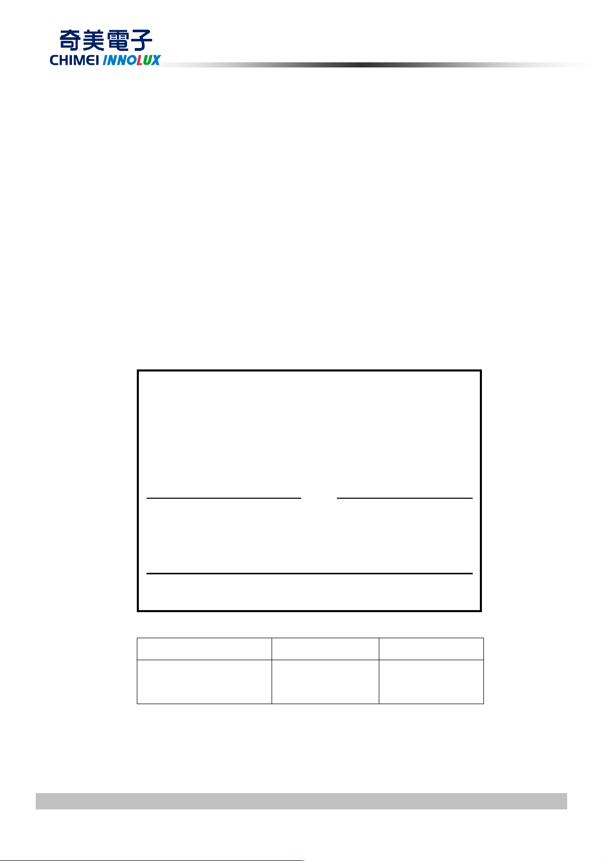
Customer:
□ Tentative Specification
□ Preliminary Specification
■ Approval Specification
MODEL NO.: V236BJ1
SUFFIX: LE1
APPROVED BY SIGNATURE
Name / Title
Note
Please return 1 copy for your confirmation with your
signature and comments.
Approved By Checked By Prepared By
Chao-Chun Chung Roger Huang Bowei Huang
Version 2.1 1 D a t e
The copyright belongs to CHIMEI InnoLux. Any unauthorized use is prohibited
14 J u ne 20 12
Page 2

PRODUCT SPECIFICATION
CONTENTS
1. GENERAL DESCRIPTION ......................................................................................................................................5
1.1 OVERVIEW ....................................................................................................................................................5
1.2 FEATURES ....................................................................................................................................................5
1.3 APPLICATION................................................................................................................................................5
1.4 GENERAL SPECIFICATIONS ........................................................................................................................5
1.5 MECHANICAL SPECIFICATIONS ..................................................................................................................6
2. ABSOLUTE MAXIMUM RATINGS ...........................................................................................................................7
2.1 ABSOLUTE RATINGS OF ENVIRONMENT....................................................................................................7
2.2 PACKAGE STORAGE....................................................................................................................................8
2.3 ELECTRICAL ABSOLUTE RATINGS..............................................................................................................8
2.3.1 TFT LCD MODULE...............................................................................................................................8
2.3.2 BACKLIGHT CONVERTER UNIT .........................................................................................................8
3. ELECTRICAL CHARACTERISTICS ........................................................................................................................9
3.1 TFT LCD MODULE.........................................................................................................................................9
3.2 BACKLIGHT CONNECTOR PIN CONFIGURATION..................................................................................... 11
3.2.1 LED LIGHT BAR CHARACTERISTICS............................................................................................... 11
3.2.2 LIGHTBAR CONNECTOR PIN ASSIGNMENT....................................................................................12
3.3 LVDS INPUT SIGNAL SPECIFICATIONS .....................................................................................................12
4. BLOCK DIAGRAM OF INTERFACE......................................................................................................................13
4.1 TFT LCD MODULE.......................................................................................................................................13
5. INPUT TERMINAL PIN ASSIGNMENT ..................................................................................................................14
5.1 TFT LCD MODULE INPUT ...........................................................................................................................14
5.3 BLOCK DIAGRAM OF INTERFACE .............................................................................................................16
5.4 LVDS INTERFACE.......................................................................................................................................17
5.5 COLOR DATA INPUT ASSIGNMENT............................................................................................................18
6. INTERFACE TIMING.............................................................................................................................................19
6.1 INPUT SIGNAL TIMING SPECIFICATIONS..................................................................................................19
6.2 POWER ON/OFF SEQUENCE.....................................................................................................................22
7. OPTICAL CHARACTERISTICS.............................................................................................................................23
7.1 TEST CONDITIONS.....................................................................................................................................23
7.2 OPTICAL SPECIFICATIONS ........................................................................................................................24
Version 2.1 2 D a t e
The copyright belongs to CHIMEI InnoLux. Any unauthorized use is prohibited
14 J u ne 20 12
Page 3

PRODUCT SPECIFICATION
8. PRECAUTIONS ....................................................................................................................................................28
8.1 ASSEMBLY AND HANDLING PRECAUTIONS .............................................................................................28
8.2 SAFETY PRECAUTIONS .............................................................................................................................28
9. DEFINITION OF LABELS......................................................................................................................................29
9.1 CMI MODULE LABEL...................................................................................................................................29
10. PACKAGING.......................................................................................................................................................30
10.1 PACKING SPECIFICATIONS......................................................................................................................30
10.2 PACKAGING METHOD..............................................................................................................................30
11. MECHANICAL CHARACTERISTIC......................................................................................................................32
Version 2.1 3 D a t e
The copyright belongs to CHIMEI InnoLux. Any unauthorized use is prohibited
14 J u ne 20 12
Page 4
PRODUCT SPECIFICATION
REVISION HISTORY
Version Date Page(New) Section Description
Ver. 2.0
Ver. 2.1
May. 29, 2012
June.14, 2012
All
17
All
5.4
The Approval Specification was first issued.
Add JEDIA LVDS format(SELLVDS pin= H or Open)
Version 2.1 4 D a t e
The copyright belongs to CHIMEI InnoLux. Any unauthorized use is prohibited
14 J u ne 20 12
Page 5
PRODUCT SPECIFICATION
1. GENERAL DESCRIPTION
1.1 OVERVIEW
V236BJ1-LE1 is a 23.6” TFT Liquid Crystal Display module with WLED Backlight unit and 30 pins 1ch-LVDS
interface. This module supports 1366 x 768 HDTV format and can display up to 16.7M (8 bit) colors. The
converter module for Backlight is not built in.
1.2 FEATURES
High brightness (250 nits)
High contrast ratio (3000:1)
Fast response time (Gray to gray average (8.5) ms)
High color saturation (NTSC 72%)
HDTV (1366 x 768 pixels) resolution, true HDTV format
DE (Data Enable) only mode
LVDS (Low Voltage Differential Signaling) interface
Optimized response time for 60 Hz frame rate
Viewing Angle: 176(H)/176(V) (CR>20) MVA Technology
RoHS compliance.
1.3 APPLICATION
Personal TV /Public Display Application
Home Theater Application
MFM Application
1.4 GENERAL SPECIFICATIONS
Item Specification Unit Note
Active Area 521.4705 (H) x 293.184 (V) mm
Bezel Opening Area 525.22 (H) x 297.22 (V) mm
Driver Element a-si TFT active matrix - -
Pixel Number 1366 x R.G.B. x 768 pixel
Pixel Pitch(Sub Pixel) 0.12725 (H) x 0.38175 (V) mm -
Pixel Arrangement RGB vertical stripe - -
Power consumption 22.679W (Max.) [Cell PW 6.349W (Max.) + BLU PW 16.33W (Max.)] Watt (2)
(1)
-
Display Colors 16.7M color
Display Operation Mode Transmissive Mode / Normally Black - -
Surface Treatment Anti-Glare coating (Haze 1.0%),Hard coating (3H) -
Note (1) Please refer to the attached drawings in chapter 11 for more information about the front and back outlines.
Note (2) Please refer sec 3.1 and 3.2 for more information of Power consumption
Version 2.1 5 D a t e
The copyright belongs to CHIMEI InnoLux. Any unauthorized use is prohibited
-
14 J u ne 20 12
Page 6

1.5 MECHANICAL SPECIFICATIONS
Item Min. Typ. Max. Unit Note
Horizontal (H) 544.3 544.8 545.3 mm (1)
PRODUCT SPECIFICATION
Module Size
Weight - 2414 - g -
Note (1) Please refer to the attached drawings for more information of front and back outline dimensions.
Vertical (V) 320.0 320.5 321.0 mm (1)
Depth (D) 10.9 11.4 11.9 mm (1)
Version 2.1 6 D a t e
The copyright belongs to CHIMEI InnoLux. Any unauthorized use is prohibited
14 J u ne 20 12
Page 7
PRODUCT SPECIFICATION
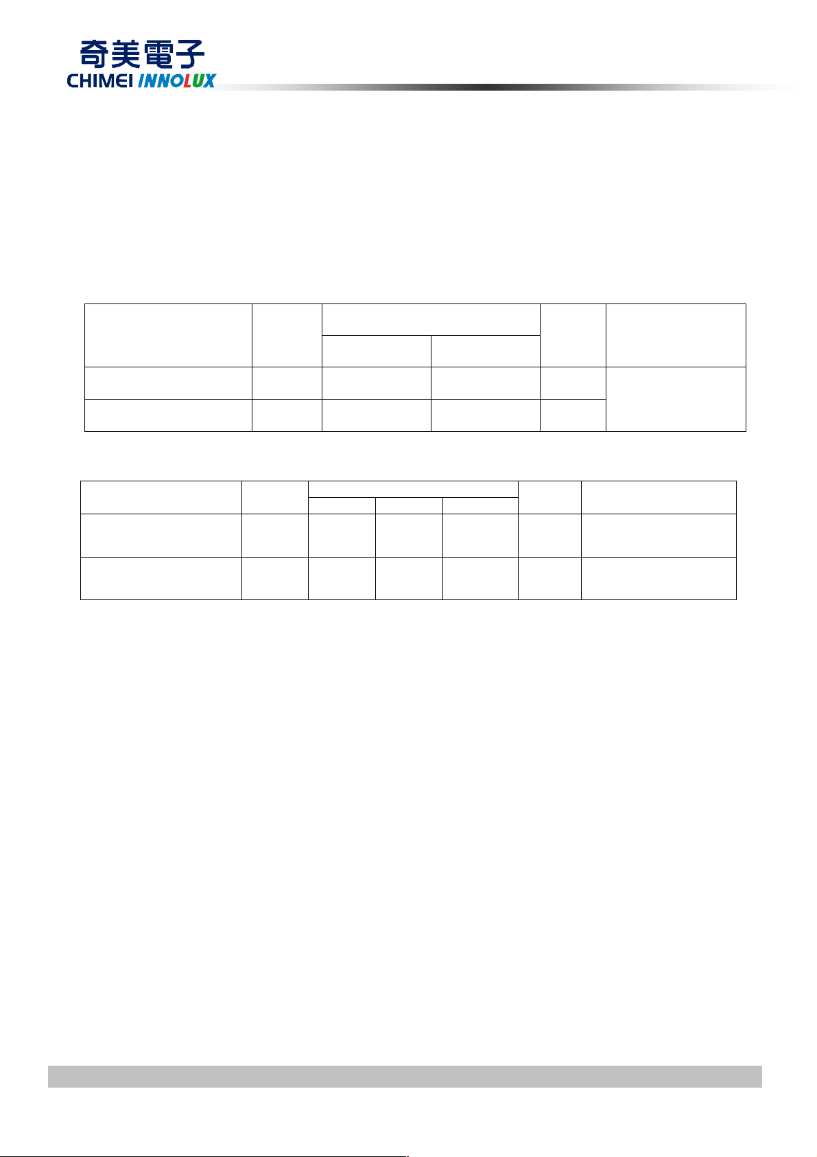
2. ABSOLUTE MAXIMUM RATINGS
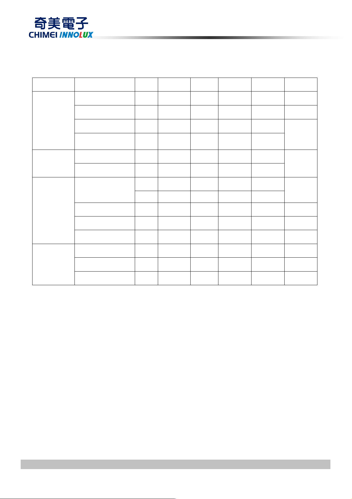
2.1 ABSOLUTE RATINGS OF ENVIRONMENT
Value
Item Symbol
Min. Max.
Storage Temperature TST -20 +60 ºC (1)
Operating Ambient Temperature TOP 0 50 ºC (1), (2)
Shock (Non-Operating) SNOP - 50 G (3), (5)
Vibration (Non-Operating) VNOP - 1.0 G (4), (5)
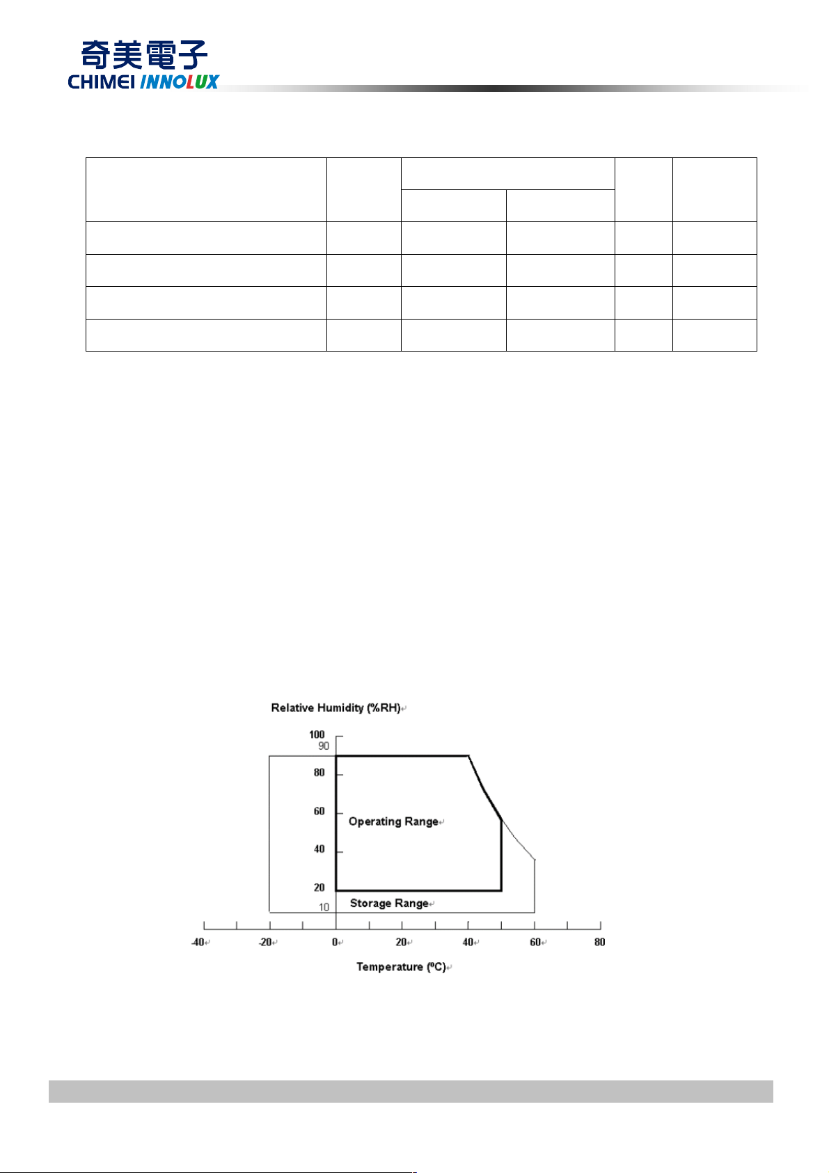
Note (1) Temperature and relative humidity range is shown in the figure below.
(a) 90 %RH Max. (Ta 40 ºC).
(b) Wet-bulb temperature should be 39 ºC Max. (Ta > 40 ºC).
(c) No condensation.
Note (2) The maximum operating temperature is based on the test condition that the surface temperature of
Unit Note
display area is less than or equal to 65 ºC with LCD module alone in a temperature controlled chamber.
Thermal management should be considered in final product design to prevent the surface temperature
of display area from being over 65 ºC. The range of operating temperature may degrade in case of
improper thermal management in final product design.
Note (3) 11 ms, half sine wave, 1 time for ± X, ± Y, ± Z.
Note (4) 10 ~ 200 Hz, 10 min, 1 time each X, Y, Z.
Note (5) At testing Vibration and Shock, the fixture in holding the module has to be hard and rigid enough so that
the module would not be twisted or bent by the fixture.
Version 2.1 7 D a t e
The copyright belongs to CHIMEI InnoLux. Any unauthorized use is prohibited
14 J u ne 20 12
Page 8
PRODUCT SPECIFICATION
LED Forward Current Per
2.2 PACKAGE STORAGE
When storing modules as spares for a long time, the following precaution is necessary.
(a) Do not leave the module in high temperature, and high humidity for a long time, It is highly recommended to
store the module with temperature from 0 to 35 at normal humidity without condensation.
(b) The module shall be stored in dark place. Do not store the TFT-LCD module in direct sunlight or fluorescent
light.
2.3 ELECTRICAL ABSOLUTE RATINGS
2.3.1 TFT LCD MODULE
Value
Item Symbol
Min. Max.
Power Supply Voltage VCC -0.3 13.5 V
Logic Input Voltage VIN -0.3 3.6 V
Unit Note
(1)
2.3.2 BACKLIGHT CONVERTER UNIT
Item Symbol
I
0 65 70 mA
Input Pin
LED Pulse Forward
Current Per Input Pin
Note (1) Permanent damage to the device may occur if maximum values are exceeded. Function operation
should be restricted to the conditions described under Normal Operating Conditions.
Note (2) Specified values are for input pin of LED light bar at Ta=25±2 (Refer to 3.2 for further
information).
F
I
FP
Min. Typ. Max.
Value
Unit Note
200 mA
(1) (2)
Duty=100%
Pulse Width 10msec.
and Duty30%
Version 2.1 8 D a t e
The copyright belongs to CHIMEI InnoLux. Any unauthorized use is prohibited
14 J u ne 20 12
Page 9
PRODUCT SPECIFICATION
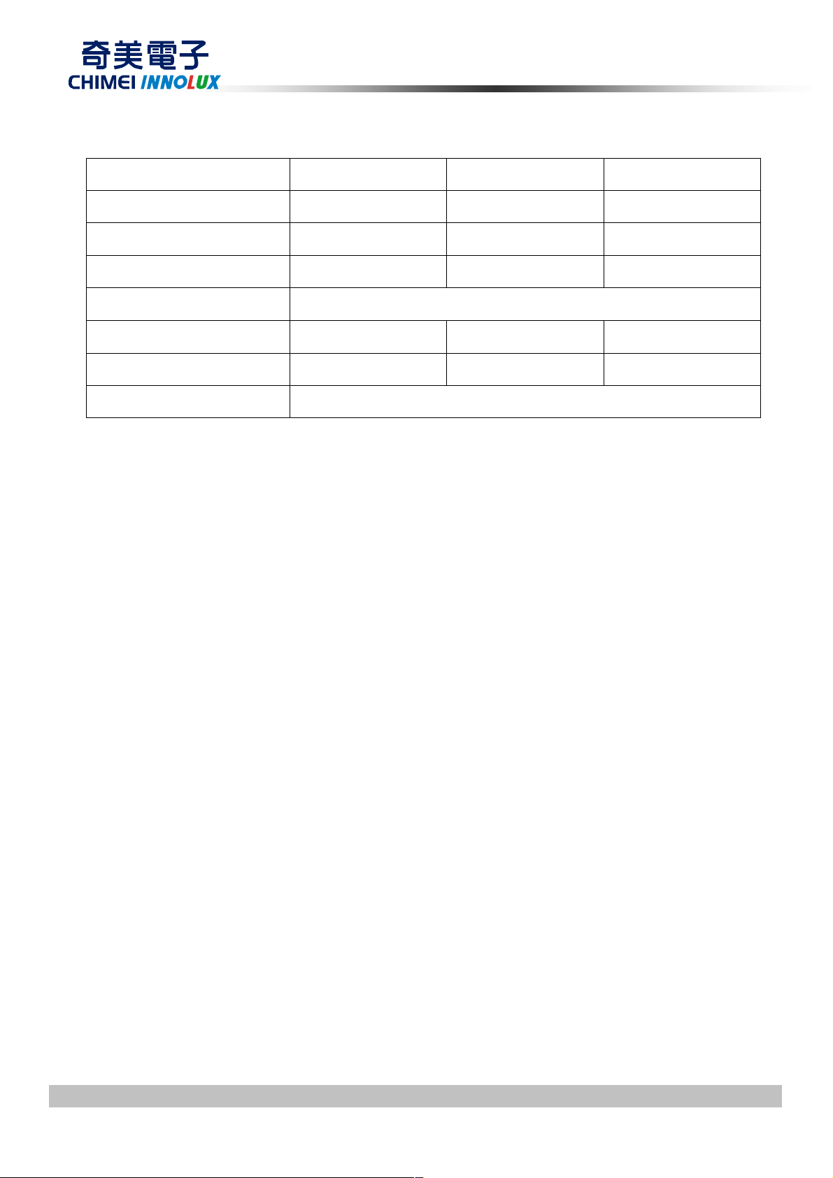
3. ELECTRICAL CHARACTERISTICS
3.1 TFT LCD MODULE
Value
Parameter Symbol
Min. Typ. Max.
Power Supply Voltage VCC 10.8 12 13.2 V (1)
Unit Note
(Ta = 25 ± 2 ºC)
Rush Current I
RUSH
Power consumption PT
V
LVTH
V
LVTL
|V
ID
Power Supply Current
Differential Input High
Threshold Voltage
Differential Input Low
Threshold Voltage
LVDS
interface
Common Input Voltage VCM 1.0 1.2 1.4 V
Differential input voltage
(single-end)
White Pattern
Horizontal Stripe
Black Pattern
Terminating Resistor RT
CMIS
interface
Input High Threshold Voltage VIH 2.7
Input Low Threshold Voltage V
IL
| 200
0
+100
4.88 6.349 Watt (3)
0.35 0.455 A
0.37 0.481 A
0.21 0.273 A
100
Note (1) The module should be always operated within the above ranges.
(3.9) A (2)
(4)
mV
-100 mV
(5)
600 mV
ohm
3.3 V
0.7 V
Note (2) Measurement condition:
Version 2.1 9 D a t e
14 J u ne 20 12
The copyright belongs to CHIMEI InnoLux. Any unauthorized use is prohibited
Page 10

PRODUCT SPECIFICATION
Vcc rising time is 470us
Note (3) The Specified Power consumption is under White pattern.
Note (4) The specified power supply current is under the conditions at Vcc = 12 V, Ta = 25 ± 2 ºC, fv = 60 Hz,
whereas a power dissipation check pattern below is displayed.
c. Horizontal Pattern
a. White Pattern
Active Area
b. Black Pattern
Active Area
Version 2.1 10 D a t e
The copyright belongs to CHIMEI InnoLux. Any unauthorized use is prohibited
14 J u ne 20 12
Page 11

PRODUCT SPECIFICATION
Note (5) The LVDS input characteristics are as follows :
3.2 BACKLIGHT CONNECTOR PIN CONFIGURATION
3.2.1 LED LIGHT BAR CHARACTERISTICS
(Ta = 25 ± 2 ºC)
Parameter Symbol
LED Light Bar Input
Voltage Per Input Pin
LED Light Bar Current
Per Input Pin
Min. Typ. Max.
V
PIN
I
PIN
25.2
--- 65 70
Value
27.9 31.4
Unit Note
(1),
V
Duty=100%,
I
=65mA
L
(1), (2)
mA
Duty=100%
(1)
Power consumption PBL
LED Life time L
LED
--- 14.5 16.33
30,000 - -
W
Hrs (3)
Duty=100%,
IL =65mA
Note (1)LED light bar input voltage and current are measured by utilizing a true RMS multimeter as shown
below:
Note (2)PBL(Typ.)= I
(Typ.) × V
PIN
(Typ.) × ( 8 ), PBL(Max.)= I
PIN
(Typ) × V
PIN
(Max.) × ( 8 ) input pins ,
PIN
Note (3)The lifetime of LED is defined as the time when LED packages continue to operate under the
conditions at Ta = 25 ±2 and I= ( 65)mA (per chip) until the brightness becomes 50% of its
original value.
Power supply
CMI Converter
Function
generator
Version 2.1 11 D a t e
The copyright belongs to CHIMEI InnoLux. Any unauthorized use is prohibited
With PWM
Function
V
PIN1, IPIN1
V
PIN(8) , IPIN(8)
LED Backlight Module
14 J u ne 20 12
Page 12
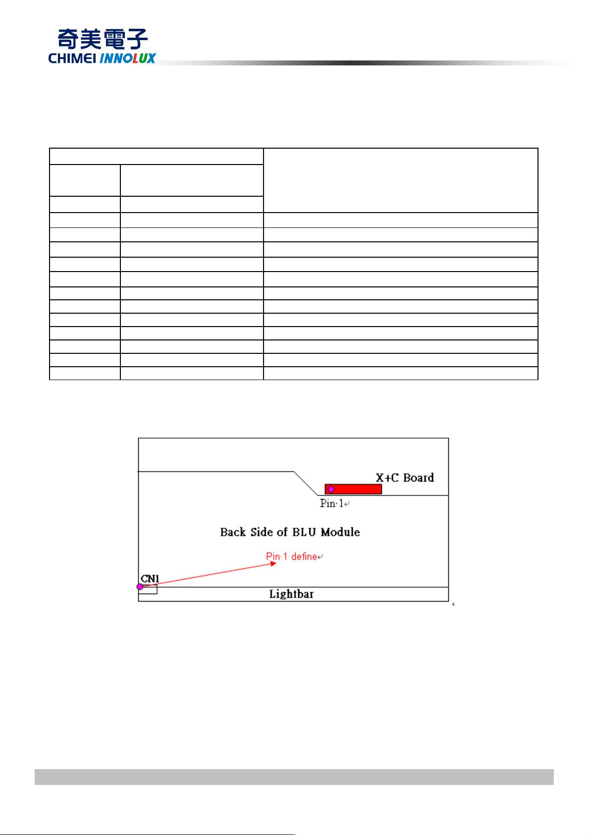
3.2.2 LIGHTBAR CONNECTOR PIN ASSIGNMENT
Connector: B-F,7083K-F12N-00L ,ENTERY( ),
161035-12041-3 P-TWO ( ),
Input connector pin assignment: CN1
Input connector CN1
(vendor)
ENTERY
Pin Function
1 LED1 Cathode of LED string
2 LED2 Cathode of LED string
3 LED3 Cathode of LED string
4 LED4 Cathode of LED string
5 NC Not connection, this pin should be open
6 VLED (27.9V) VLED
7 VLED (27.9V) VLED
8 NC Not connection, this pin should be open
9 LED5 Cathode of LED string
10 LED6 Cathode of LED string
11 LED7 Cathode of LED string
12 LED8 Cathode of LED string
(type) B-F,7083K-F12N-00L
PRODUCT SPECIFICATION
Comments
3.3 LVDS INPUT SIGNAL SPECIFICATIONS
Version 2.1 12 D a t e
The copyright belongs to CHIMEI InnoLux. Any unauthorized use is prohibited
14 J u ne 20 12
Page 13
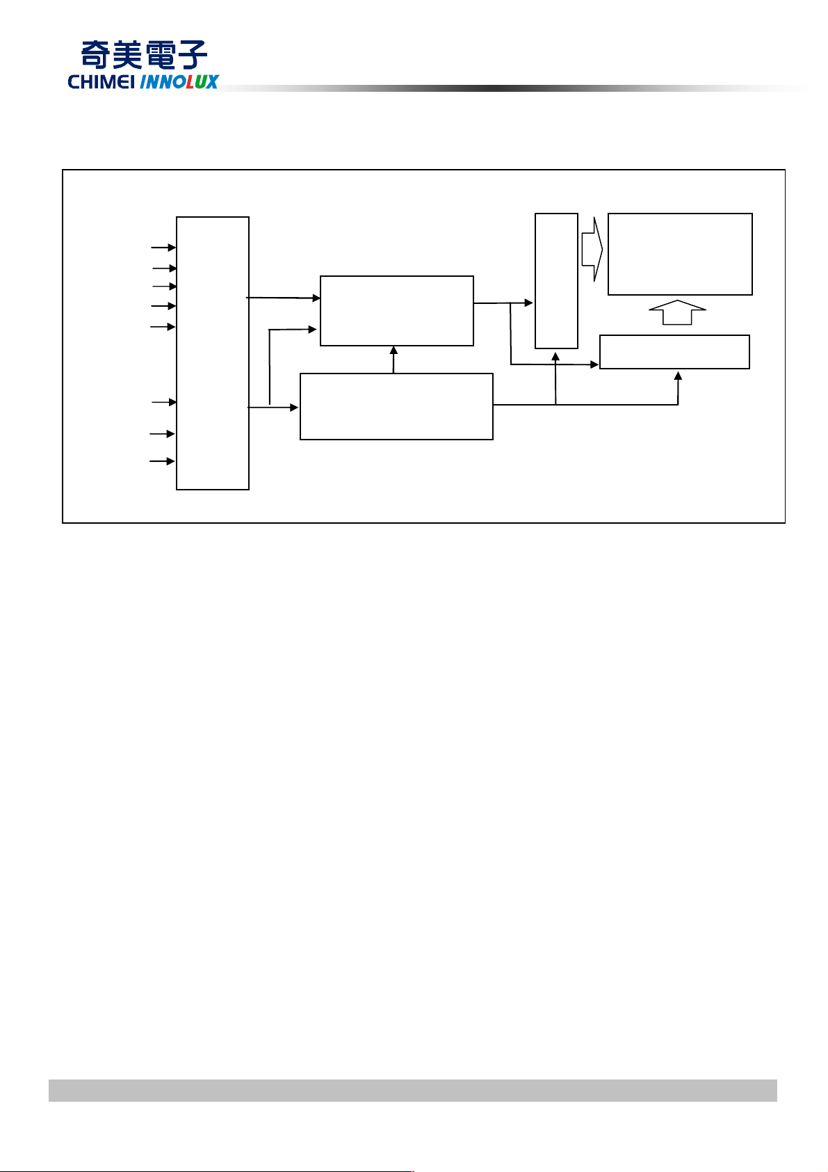
4. BLOCK DIAGRAM OF INTERFACE
SCAN DRIVER IC
4.1 TFT LCD MODULE
RX0(+/-)
RX1(+/-)
RX2(+/-)
RX3(+/-)
RXCLK(+/-)
Foxconn GS23301-0321R-7H
P-TWO=187098-30091
INPUT CONNECTOR
SELLVDS
Vcc
GND
PRODUCT SPECIFICATION
TIMING
CONTROLLER
DC/DC CONVERTER &
REFERENCE VOLTAGE
TFT LCD PANEL
(1366x3x768)
DATA DRIVER IC
Version 2.1 13 D a t e
The copyright belongs to CHIMEI InnoLux. Any unauthorized use is prohibited
14 J u ne 20 12
Page 14

PRODUCT SPECIFICATION
5. INPUT TERMINAL PIN ASSIGNMENT
5.1 TFT LCD MODULE INPUT
Connector Pin Assignment
Pin Name Description Remark
1 VCC +12.0V power supply
2 VCC +12.0V power supply
3 VCC +12.0V power supply
4 VCC +12.0V power supply
5 GND Ground
6 GND Ground
7 GND Ground
8 NC
9 SELLVDS Select LVDS Format (3)(4)
10 NC NC
11 GND Ground
12 RX0- Negative LVDS differential data input. Channel 0
13 RX0+ Positive LVDS differential data input. Channel 0
14 GND Ground
15 RX1- Negative LVDS differential data input. Channel 1
16 RX1+ Positive LVDS differential data input. Channel 1
17 GND Ground
18 RX2- Negative LVDS differential data input. Channel 2
19 RX2+ Positive LVDS differential data input. Channel 2
20 GND Ground
21 RXLCK- Negative LVDS differential clock input.
22 RXCLK+ Positive LVDS differential clock input.
23 GND Ground
24 RX3- Negative LVDS differential data input. Channel 3
25 RX3+ Positive LVDS differential data input. Channel 3
26 GND Ground
27 NC No connection (2)
28 NC No connection (2)
29 NC No connection (2)
No connection
(2)
(2)
30 GND Ground
Note (1) Connector type: (P-TWO=187098-30091 or FOXCONN= GS23301-0321R-7H )
LVDS connector pin orderdefined as follows
Version 2.1 14 D a t e
The copyright belongs to CHIMEI InnoLux. Any unauthorized use is prohibited
14 J u ne 20 12
Page 15

PRODUCT SPECIFICATION
Note (2) Reserved for internal use. Please leave it open.
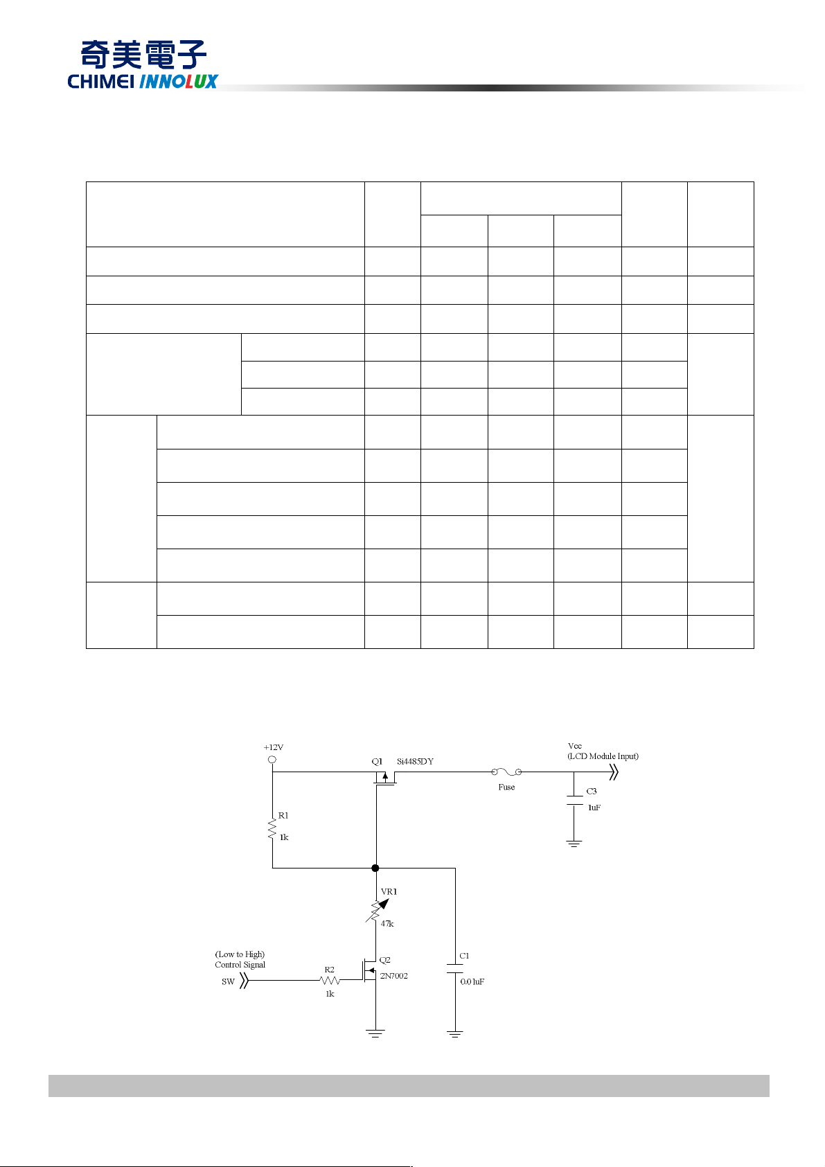
Note (3) LVDS data format Selection(0V~0.7V:VESA 2.7V~3.3V:OPENJEDIA )
Note (4) LVDS signal pin connected to the LCM side has the following diagram. R1 in the system side should
be less than 1K Ohm. (R1 < 1K Ohm)
Note (5) Suggested connector connected in seriesJAE FI-X30HL (Japan Aviation Electronics Ind., LTD.)
Version 2.1 15 D a t e
The copyright belongs to CHIMEI InnoLux. Any unauthorized use is prohibited
14 J u ne 20 12
Page 16

5.3 BLOCK DIAGRAM OF INTERFACE
PLL
51
51
100pF
R0-R7
B0-B7 DE
R0-R7
G0-G7
Rx0+
Rx1+
Rx2+
CLK+
51
51
51
51
51
51
51
RxOUT
PRODUCT SPECIFICATION
TxIN
100pF
Rx1-
Rx3+
51
100pF
100pF
Host
Graphics
Controller
LVDS Transmitter
THC63LVDM83A
(LVDF83A)
100pF
LVDS Receiver
THC63LVDF84A
DCLK
Timing
Controller
R0~R7 : Pixel R Data ,
G0~G7 : Pixel G Data ,
B0~B7 : Pixel B Data ,
DE : Data enable signal
DCLK : Data clock signal
Note (1) The system must have the transmitter to drive the module.
Note (2) LVDS cable impedance shall be 50 ohms per signal line or about 100 ohms per twist-pair line when it is
used differentially.
Version 2.1 16 D a t e
The copyright belongs to CHIMEI InnoLux. Any unauthorized use is prohibited
14 J u ne 20 12
Page 17

5.4 LVDS INTERFACE
VESA LVDS format(SELLVDS pin= L)
JEDIA LVDS format(SELLVDS pin= H or Open)
PRODUCT SPECIFICATION
R0~R7: Pixel R Data (7; MSB, 0; LSB)
G0~G7: Pixel G Data (7; MSB, 0; LSB)
B0~B7: Pixel B Data (7; MSB, 0; LSB)
DE : Data enable signal
DCLK : Data clock signal
Notes: (1) RSVD (reserved) pins on the transmitter shall be “H” or “L”.
Version 2.1 17 D a t e
The copyright belongs to CHIMEI InnoLux. Any unauthorized use is prohibited
14 J u ne 20 12
Page 18

PRODUCT SPECIFICATION
1 0 0 0 1 1 1 0 1 0 0 0 1 1 1 0 1 0 0 0 1 1 1 0 1 0 0 0 1 1 1 0 1 0 0 0 1 1 1 0 1 0 0 0 1 1 1 0 1 0 0 0 1 1 1 0 1 0 0 0 1 1 1 0 0 1 0 1 0 1 1 0 0 1 0 1 0 1 1 0 0 1 0 1 0 1 1 0 0 1 0 1 0 1 1 0 0 1 0 1 0 1 1 0 0 1 0 1 0 1 1 0 0 1 0 1 0 1 1 0 0 1 0 1 0 1 1 0 0 0 1 1 1 0 1 0 0 0 1 1 1 0 1 0 0 0 1 1 1 0 1 0 0 0 1 1 1 0 1 0 0 0 1 1 1 0 1 0 0 0 1 1 1 0 1 0 0 0 1 1 1 0 1 0 0 0 1 1 1 0 1
0 0 : : 1 1 1 0 0 0 : : 1 1 1 0 0 0 : : 1 1 1 0 0 0 : : 1 1 1 0 0 0 : : 1 1 1 0 0 0 : : 1 1 1 0 0 1 : : 0 1 1 0 1 0 : : 1 0 1 0 0 0 : : 0 0 0 0 0 0 : : 0 0 0 0 0 0 : : 0 0 0 0 0 0 : : 0 0 0 0 0 0 : : 0 0 0 0 0 0 : : 0 0 0 0 0 0 : : 0 0 0 0 0 0 : : 0 0 0 0 0 0 : : 0 0 0 0 0 0 : : 0 0 0 0 0 0 : : 0 0 0 0 0 0 : : 0 0 0 0 0 0 : : 0 0 0 0 0 0 : : 0 0 0 0 0 0 : : 0 0 0 0 0 0 : : 0 0 0
0 0 : : 0 0 0 0 0 0 : : 0 0 0 0 0 0 : : 0 0 0 0 0 0 : : 0 0 0 0 0 0 : : 0 0 0 0 0 0 : : 0 0 0 0 0 0 : : 0 0 0 0 0 0 : : 0 0 0 0 0 0 : : 1 1 1 0 0 0 : : 1 1 1 0 0 0 : : 1 1 1 0 0 0 : : 1 1 1 0 0 0 : : 1 1 1 0 0 0 : : 1 1 1 0 0 1 : : 0 1 1 0 1 0 : : 1 0 1 0 0 0 : : 0 0 0 0 0 0 : : 0 0 0 0 0 0 : : 0 0 0 0 0 0 : : 0 0 0 0 0 0 : : 0 0 0 0 0 0 : : 0 0 0 0 0 0 : : 0 0 0 0 0 0 : : 0 0 0
0 0 : : 0 0 0 0 0 0 : : 0 0 0 0 0 0 : : 0 0 0 0 0 0 : : 0 0 0 0 0 0 : : 0 0 0 0 0 0 : : 0 0 0 0 0 0 : : 0 0 0 0 0 0 : : 0 0 0 0 0 0 : : 0 0 0 0 0 0 : : 0 0 0 0 0 0 : : 0 0 0 0 0 0 : : 0 0 0 0 0 0 : : 0 0 0 0 0 0 : : 0 0 0 0 0 0 : : 0 0 0 0 0 0 : : 0 0 0 0 0 0 : : 1 1 1 0 0 0 : : 1 1 1 0 0 0 : : 1 1 1 0 0 0 : : 1 1 1 0 0 0 : : 1 1 1 0 0 0 : : 1 1 1 0 0 1 : : 0 1 1 0 1 0 : : 1 0 1
5.5 COLOR DATA INPUT ASSIGNMENT
The brightness of each primary color (red, green and blue) is based on the 8-bit gray scale data input for the
color. The higher the binary input, the brighter the color. The table below provides the assignment of the color
versus data input.
Data Signal
Color
R7 R6 R5 R4 R3 R2 R1 R0 G7 G6 G5 G4 G3 G2 G1 G0 B7 B6 B5 B4 B3 B2 B1 B0
Black
Red
Green
Basic
Colors
Gray
Scale
Of
Red
Gray
Scale
Of
Green
Gray
Scale
Of
Blue
Note (1) 0: Low Level Voltage, 1: High Level Voltage
Blue
Cyan
Magenta
Yellow
White
Red (0) / Dark
Red (1)
Red (2)
:
:
Red (253)
Red (254)
Red (255)
Green (0) / Dark
Green (1)
Green (2)
:
:
Green (253)
Green (254)
Green (255)
Blue (0) / Dark
Blue (1)
Blue (2)
:
:
Blue (253)
Blue (254)
Blue (255)
0
0
0
0
Red Green Blue
Version 2.1 18 D a t e
The copyright belongs to CHIMEI InnoLux. Any unauthorized use is prohibited
14 J u ne 20 12
Page 19
PRODUCT SPECIFICATION
6. INTERFACE TIMING
6.1 INPUT SIGNAL TIMING SPECIFICATIONS
The input signal timing specifications are shown as the following table and timing diagram. (Ta = 25 ± 2 ºC)
Signal Item Symbol
F
(=1/TC)
clkin_mod
F
F
LVDS
Receiver
Clock
LVDS
Frequency
Input cycle to cycle
jitter
Spread spectrum
modulation range
Spread spectrum
modulation frequency
Setup Time Tlvsu
Receiver
Data
Hold Time Tlvhd
Frame Rate
Vertical
Active
Display
Term
Total Tv 700 806 1050 Th
Display Tvd 768 768 768 Th
Blank Tvb 8 38 282 Th
Horizontal
Active
Display
Term
Total Th 1530 1560 2006 Tc
Display Thd 1366 1366 1366 Tc
Blank Thb 164 194 640 Tc
Min. Typ. Max. Unit Note
clkin
T
SSM
rcl
67.7 76 82 MHz
F
-2%
clkin
600
600
200 ps (2)
F
clkin
+2%
MHz
200 KHz
ps
ps
Fr5 47 50 53 Hz
Fr6 57 60 63 Hz
(3)
Tv=Tvd+Tvb
Th=Thd+Thb
Note (1) Please make sure the range of frame rate has follow the below equation
Fclkin(max) Fr6 Tv Th
Fr5 Tv Th Fclkin(min)
Version 2.1 19 D a t e
The copyright belongs to CHIMEI InnoLux. Any unauthorized use is prohibited
14 J u ne 20 12
Page 20

PRODUCT SPECIFICATION
Thb
Tc
Note (2) This module is operated in DE only mode and please follow the input signal timing diagram below
INPUT SIGNAL TIMING DIAGRAM
DE
Th
DCLK
DE
DATA
Tvd
Tv
Thd
Valid Display Data (1366 clocks)
Note (3) The input clock cycle-to-cycle jitter is defined as below figures. Trcl = I T1 – TI
Tvb
Note (4) The SSCG (Spread spectrum clock generator) is defined as below figures.
Version 2.1 20 D a t e
The copyright belongs to CHIMEI InnoLux. Any unauthorized use is prohibited
14 J u ne 20 12
Page 21

PRODUCT SPECIFICATION
14
14
14
14
14
14
Note (5) The LVDS timing diagram and setup/hold time is defined and showing as the following figures.
RXCLK+/-
RXn+/-
Tlvsu
Tlvhd
1T
LVDS RECEIVER INTERFACE TIMING DIAGRAM
Tc
5T
7T
9T
11T
13T
Version 2.1 21 D a t e
The copyright belongs to CHIMEI InnoLux. Any unauthorized use is prohibited
14 J u ne 20 12
Page 22

PRODUCT SPECIFICATION
P
100ms
T6
6.2 POWER ON/OFF SEQUENCE
(Ta = 25 ± 2 ºC)
To prevent a latch-up or DC operation of LCD module, the power on/off sequence should be as the
diagram below.
0.5T110ms
0T250ms
0T350ms
500ms T4
0V
0.1VCC
T3 T1
2
T
0.1Vcc
T4
LVDS Signals
0V
Power On
VALID
0T7T2
0T8T3
T7
T8
Option Signals
(SELLVDS)
Backlight (Recommended)
500msT5
50%
50%
5
T
T6
Note (1) The supply voltage of the external system for the module input should follow the definition of Vcc.
Note (2) Apply the lamp voltage within the LCD operation range. When the backlight turns on before the LCD
operation or the LCD turns off before the backlight turns off, the display may momentarily become
abnormal screen.
Note (3) In case of VCC is in off level, please keep the level of input signals on the low or high impedance.
Note (4) T4 should be measured after the module has been fully discharged between power off and on period.
Note (5) Interface signal shall not be kept at high impedance when the power is on.
Power ON/OFF Sequence
Version 2.1 22 D a t e
The copyright belongs to CHIMEI InnoLux. Any unauthorized use is prohibited
14 J u ne 20 12
Page 23
7. OPTICAL CHARACTERISTICS
LED Light Bar Input Current Per
7.1 TEST CONDITIONS
Item Symbol Value Unit
PRODUCT SPECIFICATION
Ambient Temperature Ta
Ambient Humidity Ha
Supply Voltage VCC 12 V
Input Signal According to typical value in "3. ELECTRICAL CHARACTERISTICS"
I
65± 1.95 mADC
Input Pin
PWM Duty Ratio D 100 %
LED Light Bar Test Converter TBD
The LCD module should be stabilized at given temperature for 1 hour to avoid abrupt temperature change during
measuring. In order to stabilize the luminance, the measurement should be executed after lighting backlight for 1
hour in a windless room.
PIN
25±2
50±10
oC
%RH
Version 2.1 23 D a t e
The copyright belongs to CHIMEI InnoLux. Any unauthorized use is prohibited
14 J u ne 20 12
Page 24
PRODUCT SPECIFICATION
7.2 OPTICAL SPECIFICATIONS
The relative measurement methods of optical characteristics are shown in 7.2. The following items should be
measured under the test conditions described in 7.1 and stable environment shown in 7.1.
Item Symbol
Contrast Ratio CR 2000 3000 - - (2)
Response Time
Center Luminance of White LC 200
White Variation
Cross Talk CT - - 4.0 % (6)
Red
Green
Color
Chromaticity
Blue
White
Gray to
gray
δW
Rx 0.638 -
Ry 0.337 -
Gx 0.309 -
Gy 0.620 -
Bx 0.149 -
By 0.059 -
Wx 0.280 -
Wy
Condition Min.
θx=0°, θy =0°
Viewing angle
at normal direction
Typ. Max. Unit Note
-
- - 1.42
Typ.
-0.03
8.5 20
250 - cd/m
0.290
Typ.
+0.03
ms
2
(7)
(1)(4)
-
(3)
(5)
Viewing Angle
Color Gamut C.G
θx+
Horizontal
θx-
θY+
Vertical
θY-
CR≥20
- 72 - % NTSC
80
80
80
80
88
88
88
88
-
Deg. (1)(4)
-
-
Version 2.1 24 D a t e
The copyright belongs to CHIMEI InnoLux. Any unauthorized use is prohibited
14 J u ne 20 12
Page 25

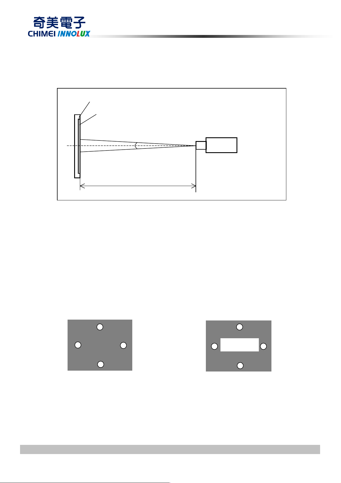
Note (1) Definition of Viewing Angle (θx, θy) :
0%
Time
Viewing angles are measured by Autronic Conoscope Cono-80
Normal
θ
x = θy = 0
θy- θy+
PRODUCT SPECIFICATION
θ
X-
= 90
x-
θx−
6 o’clock
θ
y-
= 90
y-
Note (2) Definition of Contrast Ratio (CR) :
The contrast ratio can be calculated by the following expression.
Contrast Ratio (CR) =
CR = CR (5), where CR (X) is corresponding to the Contrast Ratio of the point X at the figure in Note(7).
Note (3) Definition of Response Time (T
R
100%
90%
Gray Level 255
Optical
Response
10%
θx+
, TF):
Gray Level 0
12 o’clock direction
y+
θ
y+
= 90
pixels whiteall withLuminance Surface
pixels black all withLuminance Surface
θ
X+
x+
= 90
Gray Level 255
TR
66.67ms
Version 2.1 25 D a t e
The copyright belongs to CHIMEI InnoLux. Any unauthorized use is prohibited
TF
66.67ms
14 J u ne 20 12
Page 26
Note (4) Measurement Setup:
500
LCD
LCD
Light Shield Room
l u
Active Area
(D, W)
Active
Area
(0, 0)
The LCD module should be stabilized at given temperature for 1 hour to avoid abrupt
temperature change during measuring. In order to stabilize the luminance, the measurement
should be executed after lighting backlight for 1 hour in a windless room.
PRODUCT SPECIFICATION
odule
M
Panel
Note (5) Definition of Luminance of White (LC, L
Measure the luminance of gray level 255 at center point and 5 points
LC = L (5), where L (X) is corresponding to the luminance of the point X at the figure in Note (7).
Note (6) Definition of Cross Talk (CT):
mm
AVE
):
CS-2000T or equivalent
-
(Ambient
Luminance < 2
x)
CT = | YB – YA | / YA × 100 (%)
Where:
YA = Luminance of measured location without gray level 0 pattern (cd/m2)
YB = Luminance of measured location with gray level 0 pattern (cd/m2)
(0, 0)
Y
(D/8,W/2)
A, L
Y
Gray 128
(D/2,W/8)
A, U
Y
A, R
(7D/8,W/2)
Y
(D/8,W/2)
B, L
Y
Gray 255
(D/2,W/8)
B, U
Y
(7D/8,W/2)
B, R
Y
(D/2,7W/8)
A, D
Y
(D/2,7W/8)
B, D
(D, W)
Version 2.1 26 D a t e
The copyright belongs to CHIMEI InnoLux. Any unauthorized use is prohibited
14 J u ne 20 12
Page 27

Note (7) Definition of White Variation (δW):
Measure the luminance of gray level 255 at 5 points
δ
W = Maximum [L (1), L (2), L (3), L (4), L (5)] / Minimum [L (1), L (2), L (3), L (4), L (5)]
PRODUCT SPECIFICATION
Horizontal Line
D
D/4 D/2 3D/4
W/4
W/2
W
Vertical Line
1 2
5
3 4
: Test Point
X=1 to 5
Active Area
Version 2.1 27 D a t e
The copyright belongs to CHIMEI InnoLux. Any unauthorized use is prohibited
14 J u ne 20 12
Page 28

PRODUCT SPECIFICATION
8. PRECAUTIONS
8.1 ASSEMBLY AND HANDLING PRECAUTIONS
[ 1 ] Do not apply rough force such as bending or twisting to the module during assembly.
[ 2 ] It is recommended to assemble or to install a module into the user’s system in clean working areas. The
dust and oil may cause electrical short or worsen the polarizer.
[ 3 ] Do not apply pressure or impulse to the module to prevent the damage of LCD panel and Backlight.
[ 4 ] Always follow the correct power-on sequence when the LCD module is turned on. This can prevent the
damage and latch-up of the CMIS LSI chips.
[ 5 ] Bezel of Set can not press or touch the panel surface. It will make light leakage or scrape.
[ 6 ] Do not plug in or pull out the I/F connector while the module is in operation.
[ 7 ] Do not disassemble the module.
[ 8 ] Use a soft dry cloth without chemicals for cleaning, because the surface of polarizer is very soft and easily
scratched.
[ 9 ] Moisture can easily penetrate into LCD module and may cause the damage during operation.
[ 10 ] When storing modules as spares for a long time, the following precaution is necessary.
[ 10.1 ] Do not leave the module in high temperature, and high humidity for a long time. It is highly
recommended to store the module with temperature from 0 to 35at normal humidity without
condensation.
[ 10.2 ] The module shall be stored in dark place. Do not store the TFT-LCD module in direct sunlight or
fluorescent light.
8.2 SAFETY PRECAUTIONS
[ 1 ] If the liquid crystal material leaks from the panel, it should be kept away from the eyes or mouth. In case of
contact with hands, skin or clothes, it has to be washed away thoroughly with soap.
[ 2 ] After the module’s end of life, it is not harmful in case of normal operation and storage.
Version 2.1 28 D a t e
The copyright belongs to CHIMEI InnoLux. Any unauthorized use is prohibited
14 J u ne 20 12
Page 29
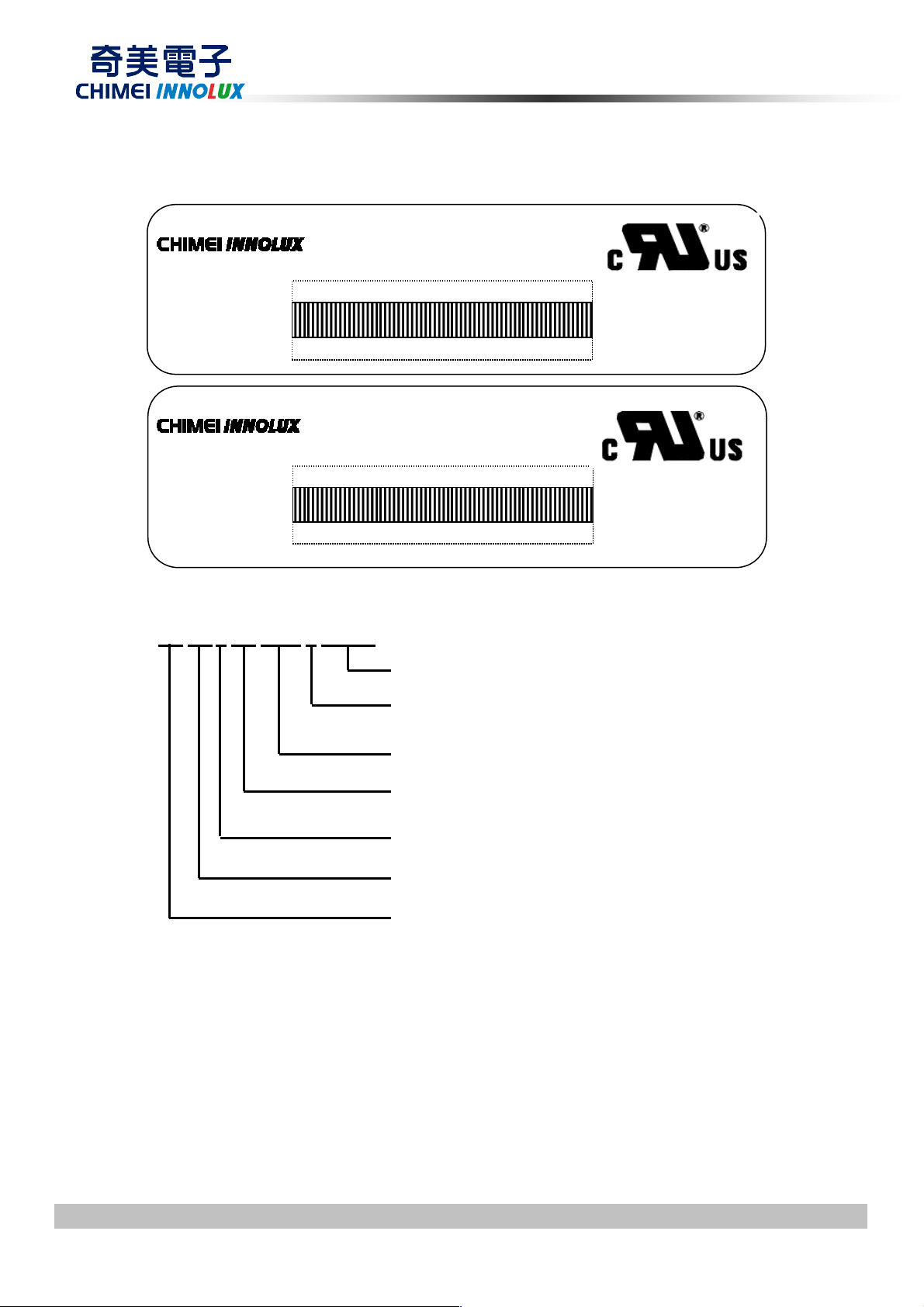
PRODUCT SPECIFICATION
X X X X X X X Y M D L N N N N
RoHS
X X X X X X X Y M D L N N N N
9. DEFINITION OF LABELS
9.1 CMI MODULE LABEL
The barcode nameplate is pasted on each module as illustration, and its definitions are as following explanation.
V236BJ1-LE1 Rev. XX
E207943
MA D E IN T A IW AN
GEMN
Model Name: V236BJ1 –LE1
Revision: Rev. XX, for example: A0, A1… B1, B2… or C1, C2…etc.
Serial ID: X X X X X X X Y M D L N N N N
Serial ID includes the information as below:
V236BJ1-LE1 Rev. XX
Serial No.
Product Line
Year, Month, Date
CMI Internal Use
CMI Internal Use
Revision
CMI Internal Use
MADE IN CHINA
LEOO(or CAPG or CANO)
RoHS
Manufactured Date:
Year : 2001=1, 2002=2, 2003=3, 2004=4…2010=0, 2011=1, 2012=2…
Month: 1~9, A~C, for Jan. ~ Dec.
Day: 1~9, A~Y, for 1st to 31st, exclude I ,O, and U.
Revision Code : Cover all the change
Serial No. : Manufacturing sequence of product
Product Line : 1 → Line1, 2 → Line 2, …etc.
Version 2.1 29 D a t e
The copyright belongs to CHIMEI InnoLux. Any unauthorized use is prohibited
14 J u ne 20 12
Page 30
10. PACKAGING
10.1 PACKING SPECIFICATIONS
(1) 11 LCD modules / 1 Box
(2) Box dimensions: 620(L) X 348(W) X 430(H) mm
(3) Weight: approximately: 29.1kg (11 modules per box)
PRODUCT SPECIFICATION
10.2 PACKAGING METHOD
(1) Carton Packing should have no failure in the following reliability test items.
Test Item Test Conditions Note
Vibration
Dropping Test 1 Corner, 3 Edge, 6 Face, 31cm Non Operation
ISTA STANDARD
Random, Frequency Range: 1 – 200 Hz
Top & Bottom: 30 minutes (+Z), 10 min (-Z),
Right & Left: 10 minutes (X)
Back & Forth 10 minutes (Y)
Non Operation
Version 2.1 30 D a t e
The copyright belongs to CHIMEI InnoLux. Any unauthorized use is prohibited
Figure 10-1 packing method Figure 10-1 packing method
14 J u ne 20 12
Page 31
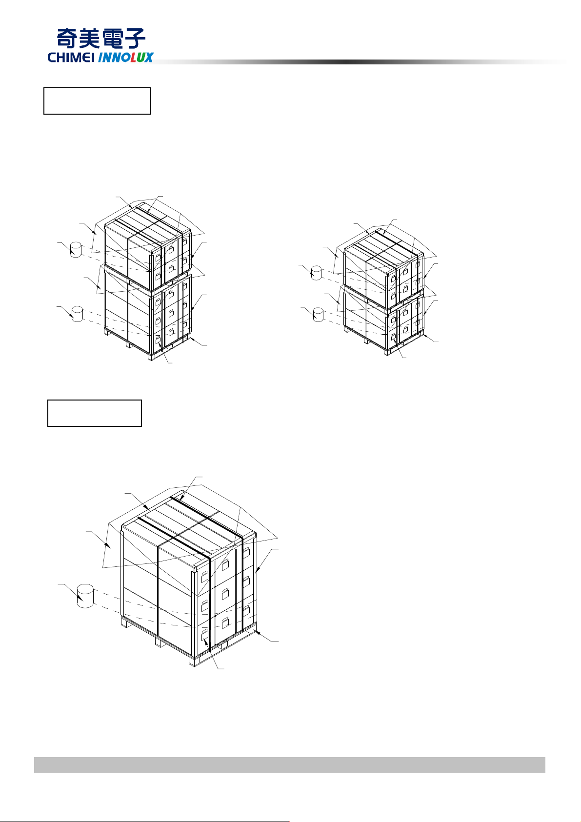
For ocean shipping
PRODUCT SPECIFICATION
Sea / Land Transportation (40ft HQ Container)
Film
Film
PE Sheet
PE Sheet
Corner Protector
(50*50*1000mm)
PP Belt
Carton label
Corner Protector
(50*50*800mm)
Corner Protector
(50*50*1250mm)
Pallet
(1250*1050*143mm)
For air transport
Sea / Land Transportation (40ft/20ft Container)
PP Belt
Carton label
Corner Protector
(50*50*800mm)
Corner Protector
(50*50*800mm)
Pallet
(1250*1050*143mm)
Film
Film
PE Sheet
PE Sheet
Corner Protector
(50*50*1000mm)
PE Sheet
Film
Corner Protector
(50*50*1000mm)
PP Belt
Corner Protector
(50*50*1250mm)
Pallet
(1250*1050*143mm)
Carton label
Figure 10-2 packing method
Version 2.1 31 D a t e
The copyright belongs to CHIMEI InnoLux. Any unauthorized use is prohibited
14 J u ne 20 12
Page 32

11. MECHANICAL CHARACTERISTIC
PRODUCT SPECIFICATION
Version 2.1 32 D a t e
The copyright belongs to CHIMEI InnoLux. Any unauthorized use is prohibited
14 J u ne 20 12
Page 33

PRODUCT SPECIFICATION
Version 2.1 33 D a t e
The copyright belongs to CHIMEI InnoLux. Any unauthorized use is prohibited
14 J u ne 20 12
 Loading...