

Page 1
Global LCD Panel Exchange Center
www.panelook.com
Issued Date: Nov. 30, 2009
Model No.: V216B1 - L03
Approval
ʳ˦
ʳ˦
TFT LCD Approval
pecification
ʳ˦ʳ˦
MODEL NO.: V216B1- L03
Customer: ________Vestel___________________
Approved by:_______________________________
Note:
1
One step solution for LCD / PDP / OLED panel application: Datasheet, inventory and accessory!
Version 3.0
www.panelook.com
Page 2
Global LCD Panel Exchange Center
www.panelook.com
Issued Date: Nov. 30, 2009
Model No.: V216B1 - L03
CONTENTS
REVISION HISTORY
1. GENERAL DESCRIPTION
1.1 OVERVIEW
1.2 FEATURES
1.3 GENERAL
1.4 MECHANICAL
2. ABSOLUTE MAXIMUM RATINGS
2.1 ABSOLUTE RATINGS OF ENVIRONMENT
2.2 TFT LCD MODULE
2.3 BACKLIGHT UNIT
3. ELECTRICAL CHARACTERISTICS
3.1 TFT LCD MODULE
3.2 CCFL (Cold Cathode Fluorescent Lamp) CHARACTERISTICS
4. BLOCK DIAGRAM
4.1 TFT LCD MODULE
5. INPUT TERMINAL PIN ASSIGNMENT
5.1 TFT LCD MODULE
5.2 LVDS DATA MAPPING TABLE
5.3 BACKLIGHT UNIT
5.4 COLOR DATA INPUT ASSIGNMENT
5.5 BLOCK DIAGRAM OF INTERFACE
6. INTERFACE TIMING
6.1 INPUT SIGNAL TIMING SPECIFICATIONS
6.2 POWER ON/OFF SEQUENCE
7. OPTICAL CHARACTERISTICS
7.1 TEST CONDITIONS
7.2 OPTICAL SPECIFICATIONS
8. DEFINITION OF LABELS
8.1 CMO MODULE LABEL
9. PACKAGING
9.1 PACKING SPECIFICATIONS
9.2 PACKING METHOD
10. PRECAUTIONS
10.1 ASSEMBLY AND HANDLING PRECAUTIONS
10.2 SAFETY PRECAUTIONS
10.3 SAFETY STANDARDS
11. MECHANICAL CHARACTERISTICS
Approval
-------------------------------------------------------
-------------------------------------------------------
-------------------------------------------------------
-------------------------------------------------------
-------------------------------------------------------
-------------------------------------------------------
-------------------------------------------------------
-------------------------------------------------------
-------------------------------------------------------
-------------------------------------------------------
-------------------------------------------------------
-------------------------------------------------------
3
4
5
7
11
12
17
21
25
26
28
29
2
One step solution for LCD / PDP / OLED panel application: Datasheet, inventory and accessory!
Version 3.0
www.panelook.com
Page 3
Global LCD Panel Exchange Center
www.panelook.com
Issued Date: Nov. 30, 2009
Model No.: V216B1 - L03
Version Date
Ver 3.0
Nov. 30,’09
Page
(New)
All
REVISION HISTORY
Section Description
All
Approval Specification was first issued.
Approval
3
One step solution for LCD / PDP / OLED panel application: Datasheet, inventory and accessory!
Version 3.0
www.panelook.com
Page 4
Global LCD Panel Exchange Center
www.panelook.com
Issued Date: Nov. 30, 2009
Model No.: V216B1 - L03
Approval
GENERAL DESCRIPTION
1.1 OVERVIEW
The V216B1-L03 model is a 21.6 inch wide TFT-LCD module with a 4-CCFL Backlight Unit and a 30-pin
1ch-LVDS interface. This module supports 1366 x 768 (16:9 wide screen) mode and displays up to 16.7
( 6-bit+Hi-FRC colors) millions colors. The inverter module for the Backlight Unit is not built in.
1.2 FEATURES
- Excellent Brightness: 400nits
- Contrast Ratio: 800:1
- Fast Response Time: 5ms
- Color Saturation: NTSC 72%
- WXGA (1366 x 768 pixels) Resolution
- DE (Data Enable) Only Mode
- LVDS (Low Voltage Differential Signaling) Interface
- Viewing Angle: 170(H)/160(V) (CR>10) TN Technology
- Color Reproduction (Nature Color)
1.3 GENERAL
Item Specification Unit Note
Active Area 477.417 (H) x 268.416 (V) (21.6” diagonal) mm
Bezel Opening Area 481.5 (H) x 272.5 (V) mm
Driver Element a-si TFT active matrix -
Pixel Number 1366 x R.G.B. x 768 pixel
Pixel Pitch (Sub Pixel) 0.1165 (H) x 0.3495 (V) mm
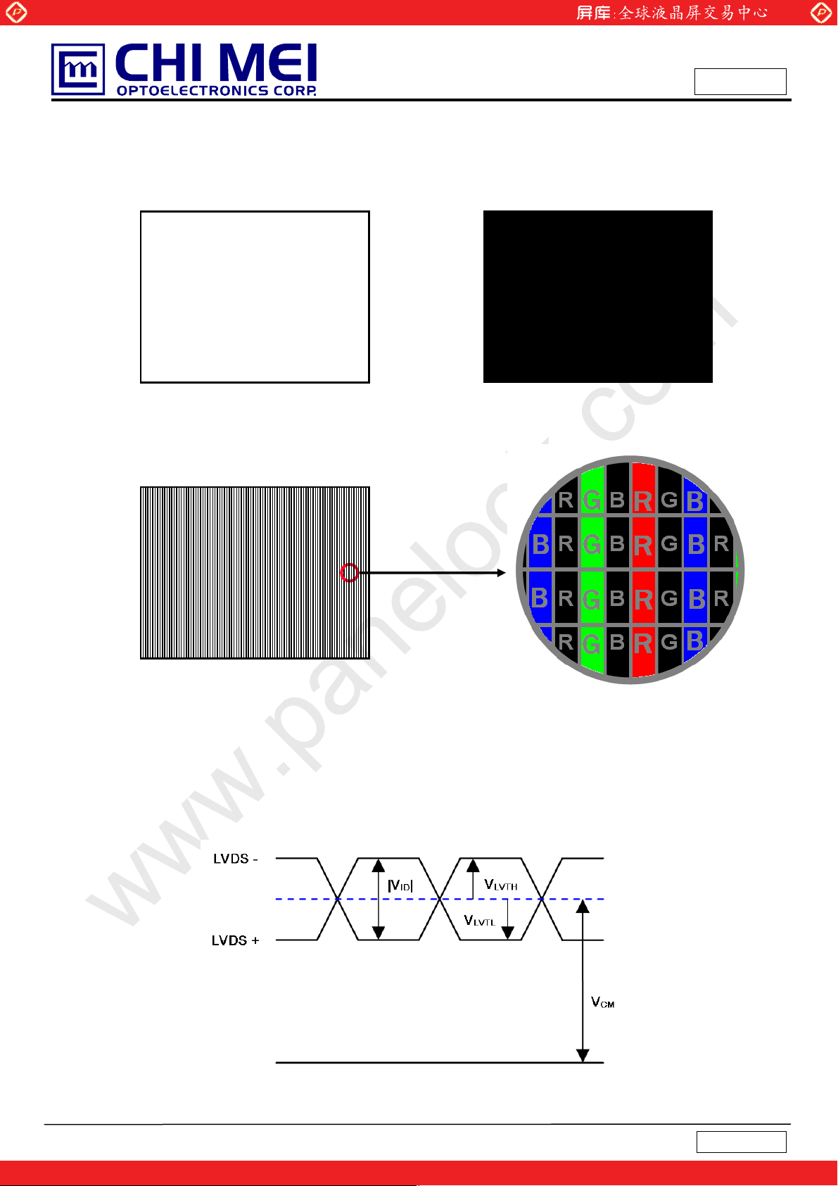
Pixel Arrangement RGB vertical stripe -
Display Colors 16.7 millions color
Display Operation Mode Transmissive mode / Normally White -
Surface Treatment Hard coating (3H), AG (Haze 25%) -
1.4 MECHANICAL
Item Min. Typ. Max. Unit Note
Horizontal(H) 500.3 501 501.7 mm
Module Size
Vertical(V) 296.4 297 297.6 mm
Depth(D) 16.8 17.3 17.8 mm To PCB cover
Weight Na 2300 Na g
4
One step solution for LCD / PDP / OLED panel application: Datasheet, inventory and accessory!
Version 3.0
www.panelook.com
Page 5
Global LCD Panel Exchange Center
www.panelook.com
Issued Date: Nov. 30, 2009
Model No.: V216B1 - L03
2. ABSOLUTE MAXIMUM RATINGS
2.1 ABSOLUTE RATINGS OF ENVIRONMENT
Item
Storage Temperature T
Operating Ambient Temperature T
Shock (Non-Operating)
Vibration (Non-Operating)
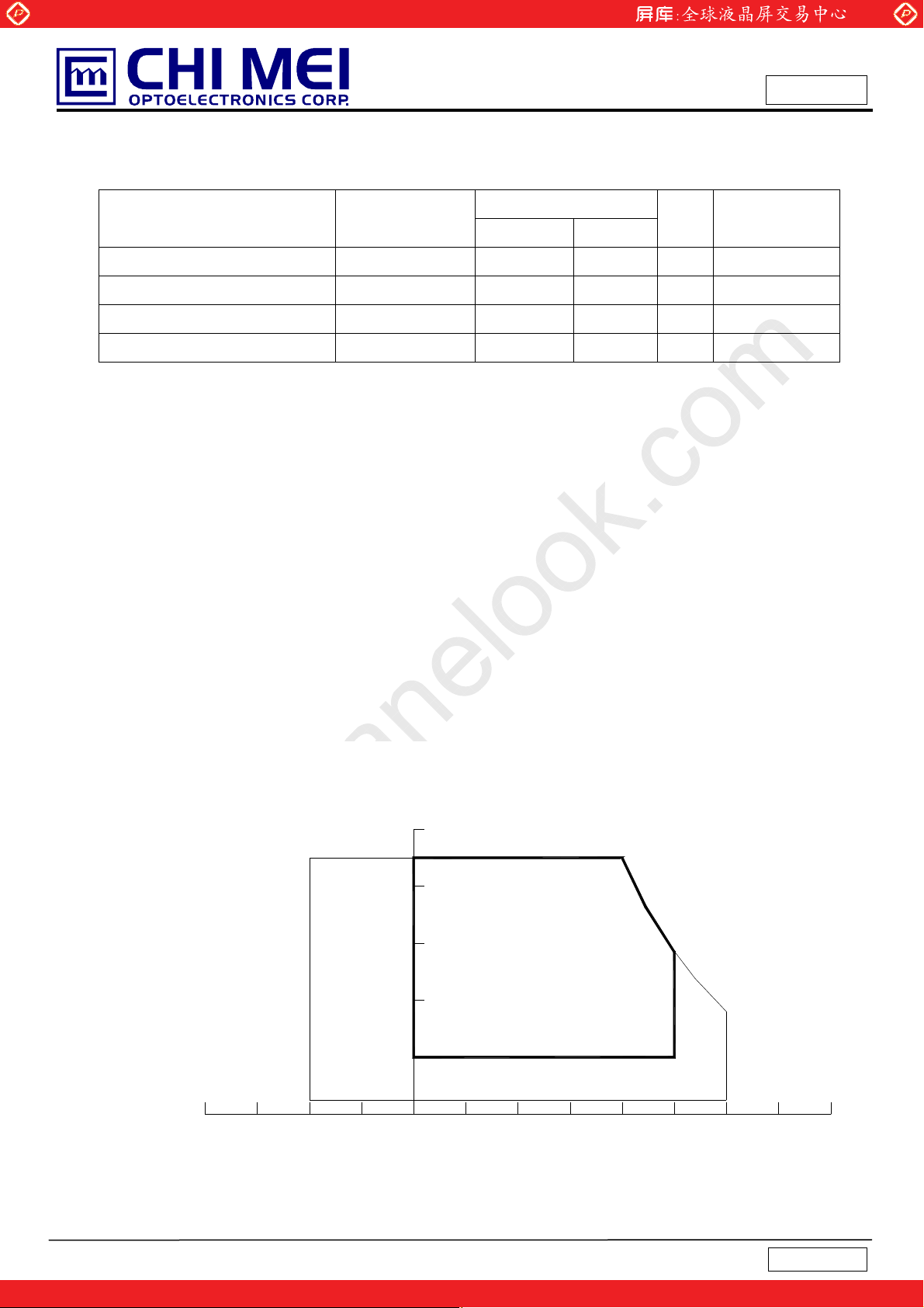
Note (1) Temperature and relative humidity range is shown in the figure below.
(a) 90% RH Max. (Ta
(b) Wet-bulb temperature should be 39
(c) No condensation.
Note (2) The maximum operating temperature is based on the test condition that the surface temperature of
display area is less than or equal to 65
Љʳ 40 к).
Symbol
ST
OP
S
NOP
V
NOP
Value
Min.
-20 +60
0 +50 к (1), (2)
к Max. (Ta > 40 к).
к with LCD module alone in a temperature controlled
- 50 G (3), (5)
- 1.0 G (4), (5)
Max.
Unit
Approval
Note
к
(1)
chamber. Thermal management should be considered in final product design to prevent the surface
temperature of display area from being over 65
in case of improper thermal management in final product design.
Note (3) 11 ms, half-sine wave, 1 time for ± X, ± Y, ± Z.
Note (4) 10 ~ 200 Hz, 10 min, 1 time each X, Y, Z.
Note (5) At testing Vibration and Shock, the fixture in holding the module has to be hard and rigid enough so
that the module would not be twisted or bent by the fixture.
Relative Humidity (%RH)
100
90
80
60
Operating Range
40
к. The range of operating temperature may degrade
20
10
Storage Range
Temperature (
5
кккк
)
One step solution for LCD / PDP / OLED panel application: Datasheet, inventory and accessory!
80 60 -20 40 0 20 -40
Version 3.0
www.panelook.com
Page 6
Global LCD Panel Exchange Center
www.panelook.com
Issued Date: Nov. 30, 2009
Model No.: V216B1 - L03
2.2 TFT LCD MODULE
Item Symbol
Power Supply Voltage Vcc -0.3 6.0 V
Input Signal Voltage VIN -0.3 3.6 V
2.3 BACKLIGHT UNIT
Item Symbol
Lamp Voltage VW
Note (1) Permanent damage to the device may occur if maximum values are exceeded. Functional
operation should be restricted to the conditions described under normal operating conditions.
Note (2) No moisture condensation or freezing.
Min. Max.
Condition
Ta = 25
Value
Te st
к Ё Ё
Unit Note
Min. Type Max. Unit Note
3000 V
RMS
Approval
6
One step solution for LCD / PDP / OLED panel application: Datasheet, inventory and accessory!
Version 3.0
www.panelook.com
Page 7
Global LCD Panel Exchange Center
www.panelook.com
Issued Date: Nov. 30, 2009
Model No.: V216B1 - L03
3. ELECTRICAL CHARACTERISTICS
3.1 TFT LCD MODULE
Parameter Symbol
Power Supply Voltage VCC
Rush Current I
White
Power Supply Current
Differential Input High
Threshold Voltage
Differential Input Low
LVDS
interface
Threshold Voltage
Common Input Voltage VCM 1.0 1.2 1.4 V
Black
Vertical Stripe
Approval
Ta = 25 ± 2 к
Value
Unit Note
Min. Typ. Max.
4.5 5.0 5.5
Ё Ё
RUSH
Ё Ё 0.4 -
Ё Ё 0.53 0.61
Ё Ё 0.50 -
V
V
LVT H
LVT L
+100
Ё Ё
Ё Ё
3.0 A (2)
-100 mV
V (1)
A
A
A
mV
(3)
(4)
|
Differential input voltage
Terminating Resistor R
CMOS
interface
Note (1) The module should be always operated within above ranges.
Note (2) Measurement Conditions:
Input High Threshold Voltage VIH 2.7
Input Low Threshold Voltage V
|V
ID
T
0
IL
200
Ё
Ё
100
Ё
Ё
600 mV
Ё
3.3 V
0.7 V
ohm
7
One step solution for LCD / PDP / OLED panel application: Datasheet, inventory and accessory!
Version 3.0
www.panelook.com
Page 8
Global LCD Panel Exchange Center
www.panelook.com
Issued Date: Nov. 30, 2009
Model No.: V216B1 - L03
Approval
470us
+5V
Vcc rising time is 470us
0.9Vcc
0.1Vcc
GND
8
One step solution for LCD / PDP / OLED panel application: Datasheet, inventory and accessory!
Version 3.0
www.panelook.com
Page 9
Global LCD Panel Exchange Center
www.panelook.com
Issued Date: Nov. 30, 2009
Model No.: V216B1 - L03
Note (3) The specified power supply current is under the conditions at Vcc = 5 V, Ta = 25 ± 2 к, fv = 60 Hz,
whereas a power dissipation check pattern below is displayed.
a. White Pattern
Active Area
c. Vertical Stripe Pattern
b. Black Pattern
Active Area
Approval
Active Area
Note (4) The LVDS input characteristics are as follows:
9
One step solution for LCD / PDP / OLED panel application: Datasheet, inventory and accessory!
Version 3.0
www.panelook.com
Page 10
Global LCD Panel Exchange Center
www.panelook.com
Issued Date: Nov. 30, 2009
Model No.: V216B1 - L03
Approval
3.2 CCFL (Cold Cathode Fluorescent Lamp) CHARACTERISTICS (
Parameter Symbol
Lamp Voltage VW
Lamp Current IL
Min. Typ. Max.
- 810 -
6.5 7.0 7.5
1250
Lamp Turn On Voltage Vs
1450
Operating Frequency FL
Lamp Life Time LBL
30 80
50000
Note (1) The waveform of the voltage output of inverter must be area-symmetric and the design of the
inverter must have specifications for the modularized lamp. The performance of the Backlight, such
as lifetime or brightness, is greatly influenced by the characteristics of the DC-AC inverter for the
lamp. All the parameters of an inverter should be carefully designed to avoid producing too much
current leakage from high voltage output of the inverter. When designing or ordering the inverter
please make sure that a poor lighting caused by the mismatch of the Backlight and the inverter
Value
Ta = 25 ± 2 к)
Unit Note
V
mA
V
V
RMS
RMS
RMS
RMS
I
= 7.0mA
L
(2), Ta = 25
(2), Ta = 0
KHz (3)
Hrs (4)
к
к
(miss-lighting, flicker, etc.) never occurs. If the above situation is confirmed, the module should be
operated in the same manners when it is installed in your instrument.
Note (2) The lamp starting voltage V
should be applied to the lamp for more than 1 second after startup.
S
Otherwise the lamp may not be turned on.
Note (3) The lamp frequency may produce interference with horizontal synchronous frequency of the
display input signals, and it may result in line flow on the display. In order to avoid interference, the
lamp frequency should be detached from the horizontal synchronous frequency and its harmonics
as far as possible.
Note (4) The life time of a lamp is defined as when the brightness is larger than 50% of its original value
and the effective discharge length is longer than 80% of its original length (Effective discharge
length is defined as an area that has equal to or more than 70% brightness compared to the
brightness at the center point of lamp.) as the time in which it continues to operate under the
condition at Ta = 25
2к and I
= 7.0 mArms.
L
10
One step solution for LCD / PDP / OLED panel application: Datasheet, inventory and accessory!
Version 3.0
www.panelook.com
Page 11

Global LCD Panel Exchange Center
(
)
4. BLOCK DIAGRAM
4.1 TFT LCD MODULE
www.panelook.com
Issued Date: Nov. 30, 2009
Model No.: V216B1 - L03
Approval
RX0(+/-)
RX1(+/-)
RX2(+/-)
RX3(+/-)
RXCLK(+/-)
SELLVDS
Vcc (5V)
GND
V/L
STARCONN 106H30-011100-A2-R
(P-TWO 196185-30041)
INPUT CONNECTOR
LAMP CONNECTOR
Inverter (W/O)
(JST, BDAMR-02VAS-3)
Lamp Connector
(YEONHO 35001HS-02L)
TIMING
CONTROLLER
DC/DC CONVERTER &
REFERENCE VOLTAGE
SCAN DRIVER IC
TFT LCD PANEL
(1366x3x768)
DATA DRIVER IC
BACKLIGHT UNIT
11
One step solution for LCD / PDP / OLED panel application: Datasheet, inventory and accessory!
Version 3.0
www.panelook.com
Page 12

Global LCD Panel Exchange Center
y
(2)
(2)
(2)
X
(2)
(2)
(2)
5. INPUT TERMINAL PIN ASSIGNMENT
5.1 TFT LCD MODULE
Pin No. S
1NC
2NC
3NC
4GND
5RX06R
7GND
8RX1-
9RX1+
10 GND
11 RX212 RX2+
13 GND
14 RXCLK15 RXCLK+
16 GND
17 RX318 RX3+
19 GND
20 NC
21
(Default:VESA)
22 NC
23 GND
24 GND
25 NC
26 VCC
27 VCC
28 VCC
29 VCC
30 VCC
mbol
Negative transmission data of pixel 0
0+
Negative transmission data of pixel 1
Negative transmission data of pixel 2
Negative transmission data of pixel 3
SELLVDS
www.panelook.com
Description
No connection
No connection
No connection
Ground
Positive transmission data of pixel 0
Ground
Positive transmission data of pixel 1
Ground
Positive transmission data of pixel 2
Ground
Negative of clock
Positive of clock
Ground
Positive transmission data of pixel 3
Ground
No connection
Select LVDS data format
No connection
Ground
Ground
No connection
Power supply: +5V
Power supply: +5V
Power supply: +5V
Power supply: +5V
Power supply: +5V
Issued Date: Nov. 30, 2009
Model No.: V216B1 - L03
Approval
Note
(3)
Note (1) Connector part no.: P-TWO 196185-30041 / STARCONN 106H30-011100-A2-R
FFC connector pin orderdefined as follows
Note (2) Reserved for CMO internal use, please leave it open
Note (3) Low = Connect to GND: JEIDA Format, High = connect to +3.3V or Open : VESA Format.
Please refer to 5.2 LVDS INTERFACE
One step solution for LCD / PDP / OLED panel application: Datasheet, inventory and accessory!
12
Version 3.0
www.panelook.com
Page 13

Global LCD Panel Exchange Center
5.2 LVDS DATA MAPPING TABLE
VESA LVDS formatΚ(SELLVDS pin=H or Open)
www.panelook.com
Issued Date: Nov. 30, 2009
Model No.: V216B1 - L03
Approval
JEDIA LVDS format
R0~R7: Pixel R Data (7; MSB, 0; LSB)
G0~G7: Pixel G Data (7; MSB, 0; LSB)
B0~B7: Pixel B Data (7; MSB, 0; LSB)
DE: Data enable signal
Κ(SELLVDS pin= L)
Notes(1) RSVD(reserved)pins on the transmitter shall be “H” or( “L” or OPEN)
13
One step solution for LCD / PDP / OLED panel application: Datasheet, inventory and accessory!
Version 3.0
www.panelook.com
Page 14

Global LCD Panel Exchange Center
5.3 BACKLIGHT UNIT
www.panelook.com
Issued Date: Nov. 30, 2009
Model No.: V216B1 - L03
Approval
14
One step solution for LCD / PDP / OLED panel application: Datasheet, inventory and accessory!
Version 3.0
www.panelook.com
Page 15

Global LCD Panel Exchange Center
www.panelook.com
Issued Date: Nov. 30, 2009
Model No.: V216B1 - L03
Approval
5.4 COLOR DATA INPUT ASSIGNMENT
The brightness of each primary color (red, green and blue) is based on the 8-bit gray scale data input for
the color. The higher the binary input, the brighter the color. The table below provides the assignment of
color versus data input.
Color
R7 R6 R5 R4 R3 R2 R1 R0 G7 G6 G5 G4 G3 G2 G1 G0 B7 B6 B5 B4 B3 B2 B1 B0
0
0
Black
Red
Green
Basic
Colors
Gray
Scale
Of
Red
Gray
Scale
Of
Green
Gray
Scale
Of
Blue
Note (1) 0: Low Level Voltage, 1: High Level Voltage
Blue
Cyan
Magenta
Yellow
White
Red(0) / Dark
Red(1)
Red(2)
:
:
Red(253)
Red(254)
Red(255)
Green(0) / Dark
Green(1)
Green(2)
:
:
Green(253)
Green(254)
Green(255)
Blue(0) / Dark
Blue(1)
Blue(2)
:
:
Blue(253)
Blue(254)
Blue(255)
0
1
1
1
0
0
0
0
0
0
0
0
0
1
1
1
1
1
1
1
1
1
0
0
0
0
0
0
0
0
0
:
:
:
:
:
:
1
1
1
1
1
1
1
1
1
0
0
0
0
0
0
0
0
0
:
:
:
:
:
:
0
0
0
0
0
0
0
0
0
0
0
0
0
0
0
0
0
0
:
:
:
:
:
:
0
0
0
0
0
0
0
0
0
Data Signal
Red Green Blue
0
0
0
0
0
0
0
0
0
0
0
0
0
0
0
0
0
0
0
0
0
1
1
1
1
1
1
1
1
1
1
1
1
1
0
0
0
0
0
0
0
0
0
0
0
0
0
0
0
0
0
1
1
1
1
1
1
0
0
0
0
0
0
0
0
0
0
0
1
1
1
1
1
1
1
1
1
1
1
1
1
1
1
1
1
1
1
1
1
1
1
1
1
1
1
0
0
0
0
0
0
0
0
0
0
0
0
0
0
1
0
0
0
0
0
0
0
0
0
1
0
0
0
:
:
:
:
:
:
:
:
:
:
:
:
:
:
:
:
:
:
0
0
0
0
1
0
1
1
1
0
0
0
0
0
1
1
1
1
0
0
0
0
1
1
1
1
1
0
0
0
0
0
0
0
0
0
0
0
0
0
0
0
0
0
0
0
0
0
0
0
0
0
0
0
:
:
:
:
:
:
:
:
:
:
:
:
:
:
:
:
:
:
1
1
1
1
0
0
0
0
0
1
1
1
1
0
0
0
0
0
1
1
1
1
0
0
0
0
0
0
0
0
0
0
0
0
0
0
0
0
0
0
0
0
0
0
0
0
0
0
0
0
0
0
0
0
:
:
:
:
:
:
:
:
:
:
:
:
:
:
:
:
:
:
0
0
0
0
0
0
0
0
0
0
0
0
0
0
0
0
0
0
0
0
0
0
0
0
0
0
0
0
0
0
0
0
:
:
:
:
0
0
0
0
0
0
0
0
0
0
0
0
:
:
:
:
1
1
1
1
1
1
0
0
0
0
0
0
:
:
:
:
0
0
0
0
0
0
0
1
1
0
0
1
1
1
1
0
0
0
0
0
0
:
:
0
0
0
0
0
0
0
0
0
1
1
0
:
:
0
1
1
0
1
1
0
0
0
0
0
0
:
:
0
0
0
0
0
0
0
0
0
0
0
0
1
1
1
1
1
1
0
0
1
1
0
0
0
0
0
0
:
:
:
:
:
:
0
0
0
0
0
0
0
0
0
0
0
0
:
:
:
:
:
:
0
0
0
0
0
0
0
0
0
0
0
0
:
:
:
:
:
:
1
1
1
1
1
1
0
0
0
0
0
0
1
1
1
1
1
1
0
0
1
1
0
0
0
0
0
0
:
:
0
0
0
0
0
0
0
0
0
0
0
0
:
:
0
0
0
0
0
0
0
0
0
0
0
0
:
:
1
1
1
1
1
1
0
0
0
0
0
0
0
0
0
0
0
0
1
1
1
1
1
1
1
1
1
1
1
1
0
0
0
0
1
1
1
1
0
0
0
0
0
0
0
0
0
0
0
0
:
:
:
:
:
:
:
:
:
:
0
0
0
0
0
0
0
0
0
0
0
0
0
0
0
0
0
0
0
0
0
0
0
0
:
:
:
:
:
:
:
:
:
:
0
0
0
0
0
0
0
0
0
0
0
0
0
0
0
0
1
0
0
0
0
1
0
0
:
:
:
:
:
:
:
:
:
:
1
0
1
1
0
1
1
1
1
1
1
1
15
One step solution for LCD / PDP / OLED panel application: Datasheet, inventory and accessory!
Version 3.0
www.panelook.com
Page 16

Global LCD Panel Exchange Center
5.5 BLOCK DIAGRAM OF INTERFACE
www.panelook.com
Issued Date: Nov. 30, 2009
Model No.: V216B1 - L03
Approval
CN1
Rx0+
-
R0-R7
-
-
Rx1+
Rx1-
Rx2+
-
Rx3+
-
Host
Graphics
Controller
CLK+
-
LVDS Transmitter
THC63LVDM83A
(LVDF83A)
51
Ө
100pF
51
Ө
51Ө
100pF
51
Ө
51
Ө
100pF
51
Ө
51
Ө
100pF
51
Ө
51
Ө
100pF
51
Ө
LVDS Receiver
THC63LVDF84A
R0-R7
-
-
DCLK
Timing
Controller
R0~R7 : Pixel R Data ,
G0~G7 : Pixel G Data ,
B0~B7 : Pixel B Data ,
DE : Data enable signal
DCLK : Data clock signal
Note (1) The system must have the transmitter to drive the module.
Note (2) LVDS cable impedance shall be 50 ohms per signal line or about 100 ohms per twist-pair line when it is
used differentially.
16
One step solution for LCD / PDP / OLED panel application: Datasheet, inventory and accessory!
Version 3.0
www.panelook.com
Page 17

Global LCD Panel Exchange Center
6. INTERFACE TIMING
www.panelook.com
Issued Date: Nov. 30, 2009
Model No.: V216B1 - L03
Approval
6.1 INPUT SIGNAL TIMING SPECIFICATIONS
The input signal timing specifications are shown as the following table and timing diagram.
Signal Item Symbol Min. Typ. Max. Unit Note
Frequency
clkin
60 76 82 MHz
F
(=1/TC)
Input cycle to
LVDS
cycle jitter
T
rcl
Ё Ё
200 ps (3)
Receiver
Clock
Spread spectrum
modulation range
clkin_mo
F
-2%
F
d
clkin
Ё
F
+2% MHz
clkin
Spread spectrum
F
LVDS
modulation frequency
SSM
Setup Time Tlvsu 600
200 KHz
Ё Ё
Receiver
Data
Hold Time Tlvhd 600
Ё Ё
Fr5 47 50 53 Hz
Vertical
Active
Frame Rate
57 60 63 Hz
F
r6
Total Tv 778 806 1000 Th Tv=Tvd+Tvb
Display
Term
Horizontal
Active
Display Tvd 768 768 768 Th
Blank Tvb 10 38
232
Total Th 1442 1560 1936 Tc Th=Thd+Thb
Display Thd 1366 1366 1366 Tc
Display
Term
Blank Thb 76 194 570 Tc
(4)
ps
(5)
ps
Ё
Th
Ё
Ё
Ё
“Enlarging Vtotal from Max 888Th to 1050Th is OK, provided that both pixel clock & Htotal are within the
specified range in the spec.”
Note (1) Please make sure the range of pixel clock has follow the below equation
Fclkin(max)
Fr5
Ѽ Tv Ѽ Th Њ Fclkin(min)
Њ Fr6 Ѽ Tv Ѽ Th
Κ
Note (2) This module is operated in DE only mode and please follow the input signal timing diagram below
17
One step solution for LCD / PDP / OLED panel application: Datasheet, inventory and accessory!
Κ
Version 3.0
www.panelook.com
Page 18

Global LCD Panel Exchange Center
www.panelook.com
Issued Date: Nov. 30, 2009
Model No.: V216B1 - L03
Approval
INPUT SIGNAL TIMING DIAGRAM
DE
Th
DCLK
DE
DATA
Tvd
Tv
Tvb
Thd
Valid display data (1366 clocks)
Note (3) The input clock cycle-to-cycle jitter is defined as below figures. Trcl = I T
– TI
1
18
One step solution for LCD / PDP / OLED panel application: Datasheet, inventory and accessory!
Version 3.0
www.panelook.com
Page 19

Global LCD Panel Exchange Center
Note (4) The SSCG (Spread spectrum clock generator) is defined as below figures.
www.panelook.com
Issued Date: Nov. 30, 2009
Model No.: V216B1 - L03
Approval
Note (5) The LVDS timing diagram and setup/hold time is defined and showing as the following figures.
RXCLK+/-
RXn+/-
Tlvsu
Tlvhd
1T
14
LVDS RECEIVER INTERFACE TIMING DIAGRAM
Tc
3T
14
5T
14
7T
14
9T
14
11T
14
13T
14
19
One step solution for LCD / PDP / OLED panel application: Datasheet, inventory and accessory!
Version 3.0
www.panelook.com
Page 20

Global LCD Panel Exchange Center
www.panelook.com
Issued Date: Nov. 30, 2009
Model No.: V216B1 - L03
Approval
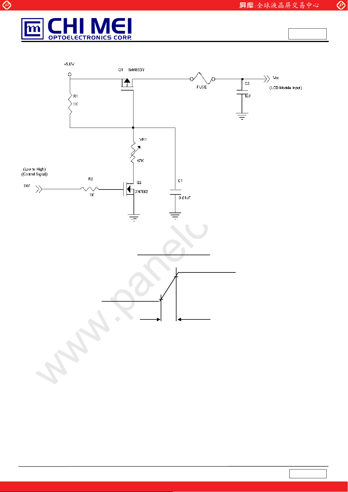
6.2 POWER ON/OFF SEQUENCE
(Ta = 25 ± 2 к)
To prevent a latch-up or DC operation of LCD module, the power on/off sequence should be as the
diagram below.
30ms
50ms
50ms
ЉЉЉЉ
T4
0V
0.5
ЉЉЉЉ
T
1
ЉЉЉЉ
ЉЉЉЉ
T
2
ЉЉЉЉ
ЉЉЉЉ
T
3
ЉЉЉЉ
0
0
500ms
0.1V
CC
3
T1
T
2
T
0.1V
T4
cc
LVDS Signals
0V
Power On
VALI D
Power Off
0
ЉЉЉЉ
T
7
ЉЉЉЉ
ЉЉЉЉ
T2
T
8
ЉЉЉЉ
T3
T7
8
T
0
Option Signals
(SELLVDS)
Backlight (Recommended)
ЉЉЉЉ
ЉЉЉЉ
T5
T
6
500ms
100ms
50%
5
T
50%
T
6
Power ON/OFF Sequence
Note (1) The supply voltage of the external system for the module input should follow the definition of Vcc.
Note (2) Apply the lamp voltage within the LCD operation range. When the backlight turns on before the LCD
operation or the LCD turns off before the backlight turns off, the display may momentarily become
abnormal screen.
Note (3) In case of Vcc is in off level, please keep the level of input signals on the low or high impedance. If
T2<0,that maybe cause electrical overstress failure.
Note (4) T4 should be measured after the module has been fully discharged between power off and on period.
Note (5) Interface signal shall not be kept at high impedance when the power is on.
20
One step solution for LCD / PDP / OLED panel application: Datasheet, inventory and accessory!
Version 3.0
www.panelook.com
Page 21

Global LCD Panel Exchange Center
7. OPTICAL CHARACTERISTICS
www.panelook.com
Issued Date: Nov. 30, 2009
Model No.: V216B1 - L03
Approval
7.1 TEST CONDITIONS
Item Symbol Value Unit
Ambient Temperature Ta
Ambient Humidity Ha
25s2
50s10
ʳ
к
%RH
Supply Voltage VCC 5.0 V
Input Signal According to typical value in "3. ELECTRICAL CHARACTERISTICS”
Inverter Current IL 7.0 mA
Inverter Driving Frequency FL 50 KHz
Dimming frequency
Minimum Duty Ratio
F
B
D
MIN
160 (type) Hz
20
%
Inverter Ampower (27-D024817)
7.2 OPTICAL SPECIFICATIONS
Item Symbol Condition Min. Typ. Max. Unit Note
Contrast Ratio CR 600 800 - (2)
Response Time
Center Luminance of White L
White Variation
Cross Talk CT 4 % (5)
Red
Green
Color
Chromaticity
Blue
TR
T
F
C
δW
=0°, θY =0°
θ
Rx 0.644 -
Ry 0.331 -
Gx 0.273 -
Gy 0.588 -
x
Viewing Angle at
Normal Direction
Bx 0.151 -
1.3 2.2
ms (3)
3.7 5.8
300 400 (4)
1.3 - (7)
Typ.
-0.03
Typ.
+0.03
(6)
By 0.061 -
White
Wx 0.285 -
Viewing
Angle
Wy
Color Gamut CG
Horizontal
Vertical
θx+
θ
x
θY+
θ
Y
68 72 %
75 85
-
75 85
CR≥10
70 80
-
70 80
0.293
Deg. (1)
Note (1) Definition of Viewing Angle (θx, θy):
Viewing angles are measured by Autronic Conoscope Cono-80
21
One step solution for LCD / PDP / OLED panel application: Datasheet, inventory and accessory!
-
NTSC
Ratio
Version 3.0
www.panelook.com
Page 22

Global LCD Panel Exchange Center
T
www.panelook.com
Issued Date: Nov. 30, 2009
Model No.: V216B1 - L03
Approval
θX- = 90
x-
6 o’clock
y-
= 90
θ
y-
Note (2) Definition of Contrast Ratio (CR):
The contrast ratio can be calculated by the following expression.
Contrast Ratio (CR) = L255 / L0
L255: Luminance of gray level 255
Normal
θx = θy = 0
θy- θy+
θx−
θx+
y+
12 o’clock direction
y+
= 90
θ
θX+ = 90
x+
L 0: Luminance of gray level 0
CR = CR (5),
CR (X) is corresponding to the Contrast Ratio of the point X at the figure in Note (7).
Note (3) Definition of Response Time (T
Gray Level 255
100%
90%
Optical
Response
10%
0%
R
TR
, TF):
Gray Level 0
T
Gray Level 255
F
ime
Note (4) Definition of Luminance of White (L
Measure the luminance of gray level 255 at center point and 5 points
):
C
LC = L (5)
L (X) is corresponding to the luminance of the point X at the figure in Note (7).
22
One step solution for LCD / PDP / OLED panel application: Datasheet, inventory and accessory!
Version 3.0
www.panelook.com
Page 23

Global LCD Panel Exchange Center
(
)
(
)
Note (5) Definition of Cross Talk (CT):
www.panelook.com
Issued Date: Nov. 30, 2009
Model No.: V216B1 - L03
Approval
CT = | Y
Where:
Y
= Luminance of measured location without gray level 0 pattern (cd/m2)
A
= Luminance of measured location with gray level 0 pattern (cd/m2)
Y
B
(0, 0)
Y
(D/8,W/2)
A, L
Y
(D/2,7W /8)
A, D
Note (6) Measurement Setup:
The LCD module should be stabilized at given temperature for 1 hour to avoid abrupt temperature
change during measuring. In order to stabilize the luminance, the measurement should be
executed after lighting Backlight for 1 hour in a windless room.
– YA | / YA × 100 (%)
B
Active Area
Gray 128
Y
Y
D,W
A, U
A, R
(D/2,W /8)
(7D/8,W/2)
(D/4,W/4)
(D/8,W/2)
Y
B, L
Y
(D/2,7W /8)
B, D
0, 0
Active Area
Gray 0
Gray 128
Y
(D/2,W /8)
B, U
Y
(7D/8,W/2)
B, R
(3D/4,3W/4)
(D,W)
Note (7) Definition of White Variation (δW):
Measure the luminance of gray level 255 at 5 points
δW = Maximum [L (1), L (2), L (3), L (4), L (5)] / Minimum [L (1), L (2), L (3), L (4), L (5)]
23
One step solution for LCD / PDP / OLED panel application: Datasheet, inventory and accessory!
Version 3.0
www.panelook.com
Page 24

Global LCD Panel Exchange Center
www.panelook.com
Issued Date: Nov. 30, 2009
Model No.: V216B1 - L03
Approval
W
W/4
W/2
3W /4
Vertical Line
Horizontal Line
D
D/4 D/2 3D/4
1 2
: Test Point
5
3 4
Active Area
X
X=1 to 5
24
One step solution for LCD / PDP / OLED panel application: Datasheet, inventory and accessory!
Version 3.0
www.panelook.com
Page 25

Global LCD Panel Exchange Center
8. DEFINITION OF LABELS
8.1 CMO MODULE LABEL
The barcode nameplate is pasted on each module as illustration, and its definitions are as following explanation.
V216B1-L03 Rev. XX
www.panelook.com
Issued Date: Nov. 30, 2009
Model No.: V216B1 - L03
Approval
CHI MEI
OPTOELECTRONICS
X X X X X X X Y M D L N N N N
E207943
MADE IN TAIWAN
GEMN
RoHS
V216B1-L03 Rev. XX
CHI MEI
OPTOELECTRONICS
X X X X X X X Y M D L N N N N
E207943
MADE IN TAIWAN
MADE IN CHINA
LEOO(or CAPG or CANO)
RoHS
(a) Model Name: V216B1-L03
(b) Revision: Rev. XX, for example: A0, A1… B1, B2… or C1, C2…etc.
(c) Serial ID: X X
X X X X X Y M D L N N N N
Serial No.
Product Line
Serial ID includes the information as below:
(a) Manufactured Date: Year: 2001=1, 2002=2, 2003=3, 2004=4….2010=0,2011=1,2012=2....
Month: 1~9, A~C, for Jan. ~ Dec.
Day: 1~9, A~Y, for 1
(b) Revision Code: Cover all the change
(c) Serial No.: Manufacturing sequence of product
(d) Product Line: 1 -> Line1, 2 -> Line 2, …etc.
Year, Month, Date
CMO Internal Use
CMO Internal Use
Revision
CMO Internal Use
st
to 31st, exclude I ,O, and U.
25
Version 3.0
One step solution for LCD / PDP / OLED panel application: Datasheet, inventory and accessory!
www.panelook.com
Page 26

Global LCD Panel Exchange Center
9. PACKAGING
9.1 PACKING SPECIFICATIONS
(1) 13 LCD TV modules / 1 Box
(2) Box dimensions: 563(L) X 417 (W) X 375 (H) mm
(3)
Weight: approximately 33Kg (13 modules per box)
9.2 PACKING METHOD
Figures 9-1 and 9-2 are the packing method
LCD TV Module
www.panelook.com
Issued Date: Nov. 30, 2009
Model No.: V216B1 - L03
Approval
Carton
Anti-Static Bag
Paper pulp mold(Bottom)
Carton Label
Carton Label
Figure.9-1 Packing Method
26
One step solution for LCD / PDP / OLED panel application: Datasheet, inventory and accessory!
Version 3.0
www.panelook.com
Page 27

Global LCD Panel Exchange Center
www.panelook.com
Issued Date: Nov. 30, 2009
Model No.: V216B1 - L03
Approval
Sea / Land Transportation
(40ft HQ Container)
Pallet Stack:L850*W1150*H2530mm
(L625mm,t=3mm)
Film
(L1120mm,t=5mm)
Carton Label
PE Sheet
PP Belt
(L1150*W850*H140mm)
Sea / Land Transportation
(40ft Container)
Pallet Stack:L850*W1150*H2155mm
(L625mm,t=3mm)
Film
(L1120mm,t=5mm)
Carton Label
PE Sheet
PP Belt
(L1150*W850*H140mm)
Figure.9-2 packing method
Air Transportation
Pallet Stack:L850*W1150*H1265mm
(L625mm,t=3mm)
Film
(L1120mm,t=5mm)
Carton Label
PE Sheet
PP Belt
(L1150*W850*H140mm)
27
One step solution for LCD / PDP / OLED panel application: Datasheet, inventory and accessory!
Version 3.0
www.panelook.com
Page 28

Global LCD Panel Exchange Center
www.panelook.com
Issued Date: Nov. 30, 2009
Model No.: V216B1 - L03
Approval
10. PRECAUTIONS
10.1 ASSEMBLY AND HANDLING PRECAUTIONS
(1) Do not apply rough force such as bending or twisting to the module during assembly.
(2) It is recommended to assemble or to install a module into the user’s system in clean working areas.
The dust and oil may cause electrical short or worsen the polarizer.
(3) Do not apply pressure or impulse to the module to prevent the damage of LCD panel and backlight.
(4) Always follow the correct power-on sequence when the LCD module is turned on. This can prevent the
damage and latch-up of the CMOS LSI chips.
(5) Do not plug in or pull out the I/F connector while the module is in operation.
(6) Do not disassemble the module.
(7) Use a soft dry cloth without chemicals for cleaning, because the surface of polarizer is very soft and
easily scratched.
(8) Moisture can easily penetrate into LCD module and may cause the damage during operation.
(9) High temperature or humidity may deteriorate the performance of LCD module. Please store LCD
modules in the specified storage conditions.
к
(10) When ambient temperature is lower than 10
response time will become slow, and the starting voltage of CCFL will be higher than that of room
temperature.
, the display quality might be reduced. For example, the
10.2 SAFETY PRECAUTIONS
(1) The startup voltage of a backlight is over 1000 Volts. It may cause an electrical shock while assembling
with the inverter. Do not disassemble the module or insert anything into the backlight unit.
(2) If the liquid crystal material leaks from the panel, it should be kept away from the eyes or mouth. In
case of contact with hands, skin or clothes, it has to be washed away thoroughly with soap.
(3) After the module’s end of life, it is not harmful in case of normal operation and storage.
10.3 SAFETY STANDARDS
The LCD module should be certified with safety regulations as follows:
(1) UL60950-1 or updated standard.
(2) IEC60950-1 or updated standard.
(3) UL60065 or updated standard.
(4) IEC60065 or updated standard.
28
One step solution for LCD / PDP / OLED panel application: Datasheet, inventory and accessory!
Version 3.0
www.panelook.com
Page 29

Global LCD Panel Exchange Center
11. MECHANICAL CHARACTERISTIC
www.panelook.com
Issued Date: Nov. 30, 2009
Model No.: V216B1 - L03
Approval
ڻႝηިҽԖϦљ
CHI MEI
29
One step solution for LCD / PDP / OLED panel application: Datasheet, inventory and accessory!
Version 3.0
www.panelook.com
Page 30

Global LCD Panel Exchange Center
www.panelook.com
Issued Date: Nov. 30, 2009
Model No.: V216B1 - L03
Approval
ڻႝηިҽԖϦљ
CHI MEI
30
One step solution for LCD / PDP / OLED panel application: Datasheet, inventory and accessory!
Version 3.0
www.panelook.com
Page 31

Global LCD Panel Exchange Center
www.panelook.com
Issued Date: Nov. 30, 2009
Model No.: V216B1 - L03
Approval
ڻႝηިҽԖϦљ
CHI MEI
31
One step solution for LCD / PDP / OLED panel application: Datasheet, inventory and accessory!
Version 3.0
www.panelook.com
 Loading...