

Page 1
Global LCD Panel Exchange Center
INNOLUX DISPLAY CORPORATION
TM315GW01 V.0 LCD OPEN CELL SPECIFICATION
●
) Preliminary Specification
(
●
) Final Specification
(
www.panelook.com
Approved by Checked by Prepared by
Innolux Display Corporation,
No.160 Kesyue Rd., Chu-Nan Site, Hsinchu Science Park,
Chu-Nan 350, Miao-Li County, Taiwan
Tel: 886-37-586000 Fax: 886-37-586060
Document Number: TM315GW01 V.0-DR5
One step solution for LCD / PDP / OLED panel application: Datasheet, inventory and accessory!
www.panelook.com
Page 2
Global LCD Panel Exchange Center
INNOLUX DISPLAY CORPORATION
TM315GW01 V.0 LCD OPEN CELL SPECIFICATION
Department Prepared by Checked by
www.panelook.com
PD
MKT
TD
EE
ME
RA
Innolux Display Corporation
Document Number: TM315GW01 V.0-DR5
One step solution for LCD / PDP / OLED panel application: Datasheet, inventory and accessory!
www.panelook.com
Page 3
Global LCD Panel Exchange Center
www.panelook.com
SPEC NO.
PAGE
Version: 1.2
Record of Revision
Version Revise Date P age Content
1.0 2011/5/5
1.1 2011/6/14 6 Update LVDS connector supplier part number
1.2 2011/6/14 19~21 Update label and packing
All First edition to all Spec.
TM315GW01 V.0
3/22
InnoLux copyright
All rights reserved,
Copying forbidden.
One step solution for LCD / PDP / OLED panel application: Datasheet, inventory and accessory!
www.panelook.com
Page 4
Global LCD Panel Exchange Center
www.panelook.com
SPEC NO.
PAGE
TM315GW01 V.0
4/22
Contents:
A. General Specification 5
B. Electrical Specifications 6
1. Pin assignment
2. Absolute maxi mum ratings
3. Electrical characteristics
a. Typical operating conditions
b. Display color vs. input data signals
6
8
9
9
12
c. Input signal timing
d. Display position
C. Optical specifications
13
14
15
E. Safety 18
F. Display quality 18
G. Handling precaution 18
H. Label 19
I. Packing specification 20
J. Mechanical drawings 22
One step solution for LCD / PDP / OLED panel application: Datasheet, inventory and accessory!
www.panelook.com
Page 5
Global LCD Panel Exchange Center
www.panelook.com
SPEC NO.
PAGE
TM315GW01 V.0
5/22
A. General specification
1. OVERVIEW
TM315GW01 V.0 is a 31.5” TFT Liquid Crystal Display open cell. This open cell supports 1366 x 768 WXGA
format and can display true 16.7M colors (8-bit).
2. CHARACTERISTICS
CHARACTERISTICS ITEMS
Screen size (in)
Pixel (lines)
Active area (mm)
Sub - Pixel pitch (mm)
SPECIFICATIONS
31.5
1366X 768
697.685 (H) X 392.256(V) (31.5’’)
0.17025 (H) X 0.51075 (V)
Color configuration
Weight (g)
Physical Size (mm)
Display Mode
Contrast Ratio
Glass thickness (Array/CF) (mm)
Viewing Angle (CR>10)
Color Chromaticity
Cell Transparency (%)
R, G, B vertical stripe
1180
716.0 (H) X 414.4 (W) X1.83 (D) Typ.
Transmissive mode/Normally black
(3000:1) Typ.
(Typical value measure at INL’s module)
0.7 / 0.7
+89/-89(H), +89/-89(V) Typ.
(Typical value measure at INL’s module)
R= 0.647, 0.337
G= 0.292, 0.600
B= 0.138, 0.091
W= 0.317, 0.338 (With C source)
4.62%Typ.
(Typical value measure at INL’s module)
Anti-glare coating, 707.8(H)407.7(W)
F9,
Polarizer (CF side)
Polarizer (TFT side)
Hardness:3H
Anti-glare coating, 706.5(H)407.2(W)
F9,
One step solution for LCD / PDP / OLED panel application: Datasheet, inventory and accessory!
www.panelook.com
Page 6
Global LCD Panel Exchange Center
www.panelook.com
SPEC NO.
PAGE
B. Electrical specifications
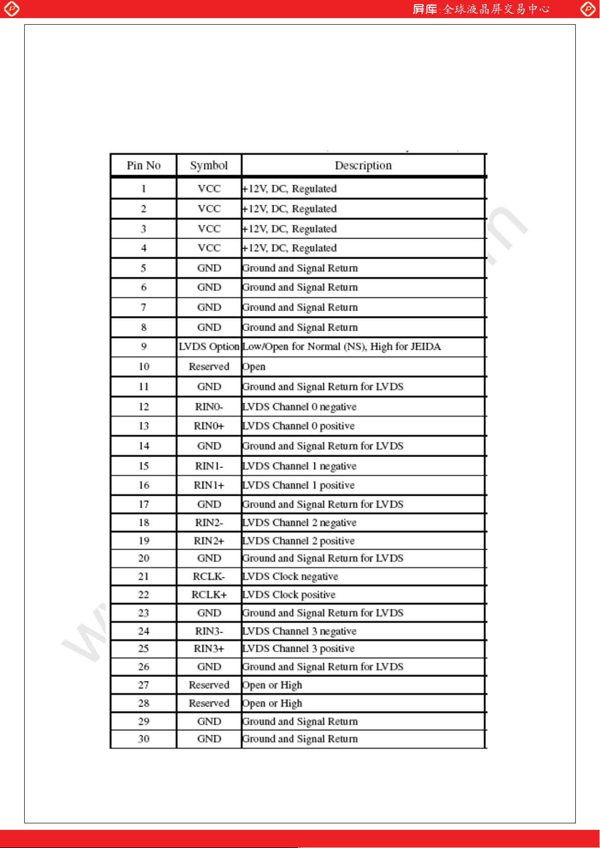
1. Pin assignment
Connector
FOXCONN GS23302-1311S-7F or mechanical interface equivalent connector.
TM315GW01 V.0
6/22
One step solution for LCD / PDP / OLED panel application: Datasheet, inventory and accessory!
www.panelook.com
Page 7
Global LCD Panel Exchange Center
www.panelook.com
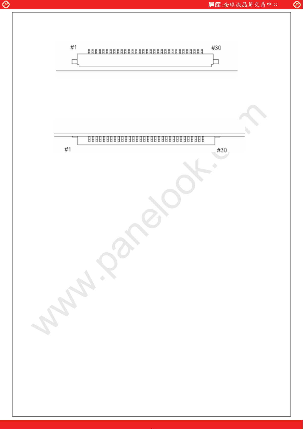
Top view of LVDS connector
SPEC NO.
PAGE
TM315GW01 V.0
7/22
Rear view of LVDS connector
ʳ
One step solution for LCD / PDP / OLED panel application: Datasheet, inventory and accessory!
www.panelook.com
Page 8

Global LCD Panel Exchange Center
www.panelook.com
2. Absolute maximum ratings
Parameter Symbol
LCD drive voltage Vcc -0.3 - 14.0 V At 25°C
Input signal voltage VLH -0.3 - 3.6 V At 25°C
BLU Input voltage VDDB -0.3 - 28 V At 25°C
Operating temperature Top 0 - 50 °C Note 1
Operating Humidity Hop 10 - 90 %RH
Storage temperature TST -20 - 60 °C Note 2
Values
Min.
Typ.
SPEC NO.
PAGE
Max.
TM315GW01 V.0
8/22
Unit
Remark
Storage Humidity HST
Note 1: The relative humidity must not exceed 90% non-condensing at temperatures of 40°C or less.
At temperatures greater than 40°C, the wet bulb temperature must not exceed 39°C.
Note 2: The unit should not be exposed to corrosive chemicals.
10 -
90 %RH
Relative Humidity (%RH)
100
90
80
Storage Range
70
60
50
40
Operation Range
30
20
10
0
-40
0 20 40 60 80 -20
Temperature (ºc)
One step solution for LCD / PDP / OLED panel application: Datasheet, inventory and accessory!
www.panelook.com
Page 9

Global LCD Panel Exchange Center
www.panelook.com
3. Electrical characteristics
a. Typical operating conditions
Item Symbol Min. Typ. Max. Unit Remark
LCD Input Voltage
LCD Permissive Power Input Ripple
LCD Input Current
Power Consumption
LCD Rush Current
Logic Input
Common Mode Voltage
Black
White
Mosaic
SPEC NO.
PAGE
V
cc
V
RF
10.8 12 13.2
- - 0.4
TM315GW01 V.0
9/22
Icc - 300 400
Icc - 450 550
I
cc
Pc
I
Rush
VCM
- 375 475
- 5.4 7.26
- - 3
1.10 1.25 1.40
V
V
mA
W Note 2
A Note 4
V
Note 1
Note 2
Note 3
Voltage
LVDS:
IN+, IN-
Differential Input Voltage
Threshold Voltage (High)
Threshold Voltage (Low)
VID
VTH
VTL
100 - 600
- - 100
-100 - -
mV
mV Note 5
mV Note 5
Note 1 : The specified current is under the Vcc =12V, 25 °C, fv=60Hz (frame frequency) condition
whereas black pattern is displayed.
Note 2 : The specified current is under the Vcc =12V, 25 °C, fv=60Hz (frame frequency) condition
whereas white pattern is displayed.
Note 3 : The specified current is under the Vcc =12V, 25 °C, fv=60Hz (frame frequency) condition
whereas mosaic pattern(black & white [8*6] ) is displayed.
White : 255 Gray
Black : 0 Gray
One step solution for LCD / PDP / OLED panel application: Datasheet, inventory and accessory!
www.panelook.com
Page 10
Global LCD Panel Exchange Center
www.panelook.com
Note 4 : test condition :‘
(1) V
(2) Pattern: Mosaic pattern
(3) Test circuit
= 12 V, VDD rising time = 470 μs ± 10%
DD
90
%
10%
V
12 V
DD
R1
47K
SPEC NO.
PAGE
TM315GW01 V.0
10/22
Ton=470 Ӵs 10%
M1
2SK1059
FUSE
VDD (
C1
1uF
LCD INPUT)
CONTROL SIGNAL
(HIGH to LOW )
12V
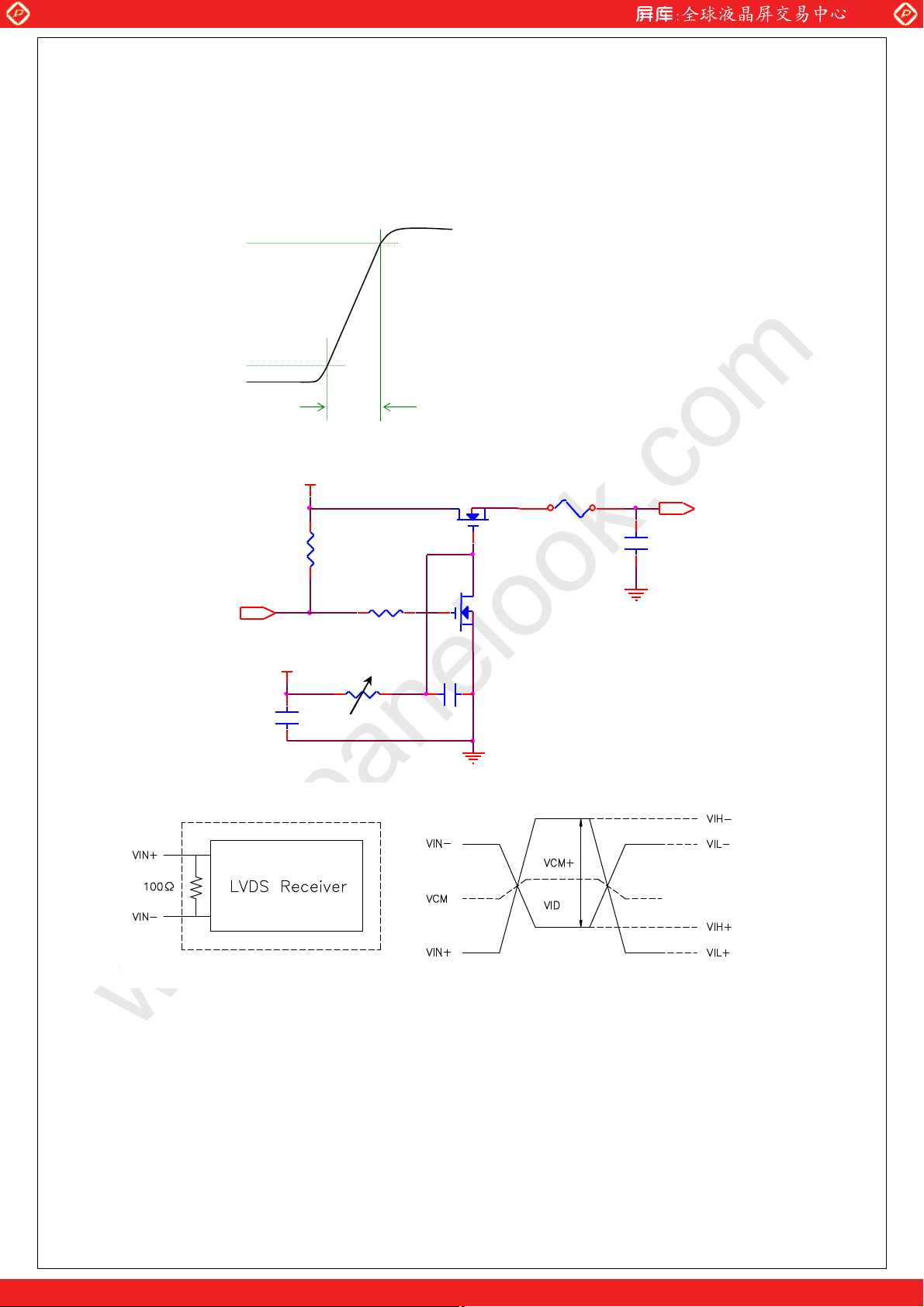
Note 5: LVDS signal definition
VIN+ = Positive differential DATA & CLK Input
VIN- = Negative differential DATA & CLK Input
VID = VIN+ – VIN- ,
C3
1uF
R3
47K
R2
1K
M2
2SK1399
C2
10000pF
ΔVCM =
ΔVID =
VID+ =
VID- =
VCM = (VIN
VCM+ = (VIH
VCM- = (VIL
Ψ
VCM+–VCM-Ψ,
Ψ
VID+–VID-Ψ,
Ψ
VIH+–VIH-Ψ,
Ψ
VIL+–VIL-Ψ,
+VIN-)/2,
+
+VIH-)/2,
+
+VIL-)/2,
+
One step solution for LCD / PDP / OLED panel application: Datasheet, inventory and accessory!
www.panelook.com
Page 11

Global LCD Panel Exchange Center
www.panelook.com
Note 6 : Power on sequence for LCD V
T1
Panel Power
Supply V
Interface
Signals
DC
10%
90%
90% 90%
T2
DD
Valid Interface Data
90%
90%
SPEC NO.
PAGE
90%
T6
T5
10%
TM315GW01 V.0
11/22
T7
10%
Backlight Power
Supply
T3 T4
Parameter Value Unit
Min Typ Max ms
T1 0.1 - 30 ms
T2 0.1 - 50 ms
T3 200 - - ms
T4 10 - - ms
T5 0.1 - 50 ms
T6 - 300 ms
T7 500 - - ms
One step solution for LCD / PDP / OLED panel application: Datasheet, inventory and accessory!
www.panelook.com
Page 12
Global LCD Panel Exchange Center
www.panelook.com
SPEC NO.
PAGE
TM315GW01 V.0
12/22
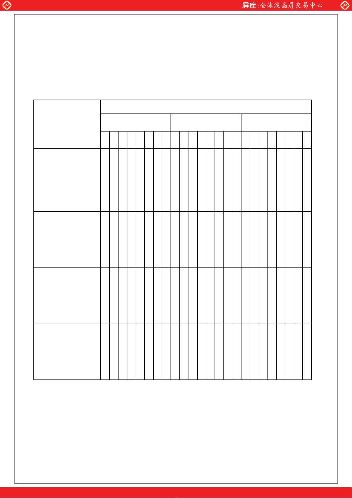
b. Display color vs. input data signals
The brightness of each primary color (red, green and blue) is based on the 8-bit gray scale data input
for the color; the higher the binary input, the brighter the color. The table below provides a reference for
color versus data input.
Color
MSB LSB MSB LSB MSB LSB
R7 R6 R5 R4 R3 R2 R1 R0
Red Green Blue
Input color data
G7 G6 G5 G4 G3 G2 G1 G0
B7 B6 B5 B4 B3 B2 B1 B0
Basic
colors
Black
Red(255)
Green(255)
Blue(255)
Cyan
Magenta
Yellow
White
0
0
1
1
1
1
1
1
0
0
0
0
0
0
0
0
0
0
0
0
0
0
0
0
0
0
1
1
1
1
1
1
1
1
1
1
1
1
1
1
1
1
1
1
0
0
1
0
0
0
1
1
1
0
0
1
0
0
1
1
0
0
0
0
1
1
0
0
0
1
1
1
1
1
1
1
0
0
0
0
0
0
0
0
1
1
1
1
0
0
0
0
1
1
1
1
0
0
0
0
1
1
1
1
1
1
1
1
0
0
0
0
1
1
0
0
1
1
0
0
1
1
1
1
0
0
0
0
0
0
0
0
0
1
1
1
1
1
1
1
1
1
0
0
0
1
1
1
0
0
0
0
0
0
0
0
0
0
0
0
1
1
1
1
1
1
1
1
1
0
0
0
1
1
1
0
0
0
0
0
0
1
1
1
1
1
1
0
0
1
1
0
Red
Green
Red(000) dark
Red(001)
Red(002)
:
Red(253)
Red(254)
Red(255) bright
Green(000)dark
Green(001)
Green(002)
:
Green(253)
Green(254)
Green(255)
bright
0
0
0
0
0
0
0
0
0
0
0
0
0
0
:
:
:
:
1
1
1
1
1
1
1
1
1
1
1
1
1
1
1
0
0
0
0
0
0
:
:
0
0
0
0
0
0
0
0
0
0
0
0
0
0
0
:
:
0
0
0
0
0
0
0
0
0
0
1
0
:
:
:
:
1
0
1
1
1
1
0
0
0
0
0
0
:
:
0
0
0
0
0
0
0
0
1
0
0
0
0
0
:
:
:
1
0
0
0
0
0
1
0
0
0
0
0
0
0
0
0
0
0
:
:
:
1
1
0
1
1
0
1
1
0
0
0
0
0
0
0
0
0
0
:
:
0
0
0
0
0
0
0
0
0
0
0
0
0
0
0
0
0
0
:
:
1
1
1
1
1
1
1
1
1
0
0
0
0
0
0
:
:
:
0
0
0
0
0
0
0
0
0
0
1
0
:
:
:
0
1
1
1
1
1
0
0
0
0
0
0
0
0
0
0
0
0
0
0
0
0
0
:
:
0
0
0
0
0
0
0
0
1
0
0
0
:
:
1
0
0
0
1
0
:
:
0
0
0
0
0
0
0
0
0
0
0
0
:
:
0
0
0
0
0
0
0
0
0
0
0
0
0
0
0
:
:
0
0
0
0
0
0
0
0
0
0
0
0
0
0
0
0
0
0
:
:
0
0
0
0
0
0
0
0
0
0
0
0
0
0
0
:
:
:
:
0
0
0
0
0
0
0
0
0
0
0
0
:
:
0
0
0
0
0
0
Blue(000) dark
Blue(001)
Blue(002)
Blue
Blue(253)
Blue(254)
Blue(255) bright
:
0
0
0
0
0
0
0
0
0
0
0
0
0
:
:
:
:
0
0
0
0
0
0
0
0
0
0
0
0
0
0
0
0
0
0
:
:
0
0
0
0
0
0
0
0
0
0
0
:
:
0
0
0
0
0
0
0
0
0
0
0
0
:
:
:
0
0
0
0
0
0
0
0
0
0
0
0
0
0
0
:
:
0
0
0
0
0
0
0
0
0
0
0
0
0
0
0
:
:
:
0
0
0
0
0
0
0
0
0
0
0
0
0
0
0
:
:
:
1
1
1
1
1
1
1
1
1
0
0
0
0
0
0
0
0
0
:
:
1
1
1
1
1
1
1
1
1
0
0
1
0
0
1
:
:
:
1
0
0
1
1
1
0
0
0
0
0
0
One step solution for LCD / PDP / OLED panel application: Datasheet, inventory and accessory!
www.panelook.com
Page 13
Global LCD Panel Exchange Center
www.panelook.com
SPEC NO.
PAGE
TM315GW01 V.0
13/22
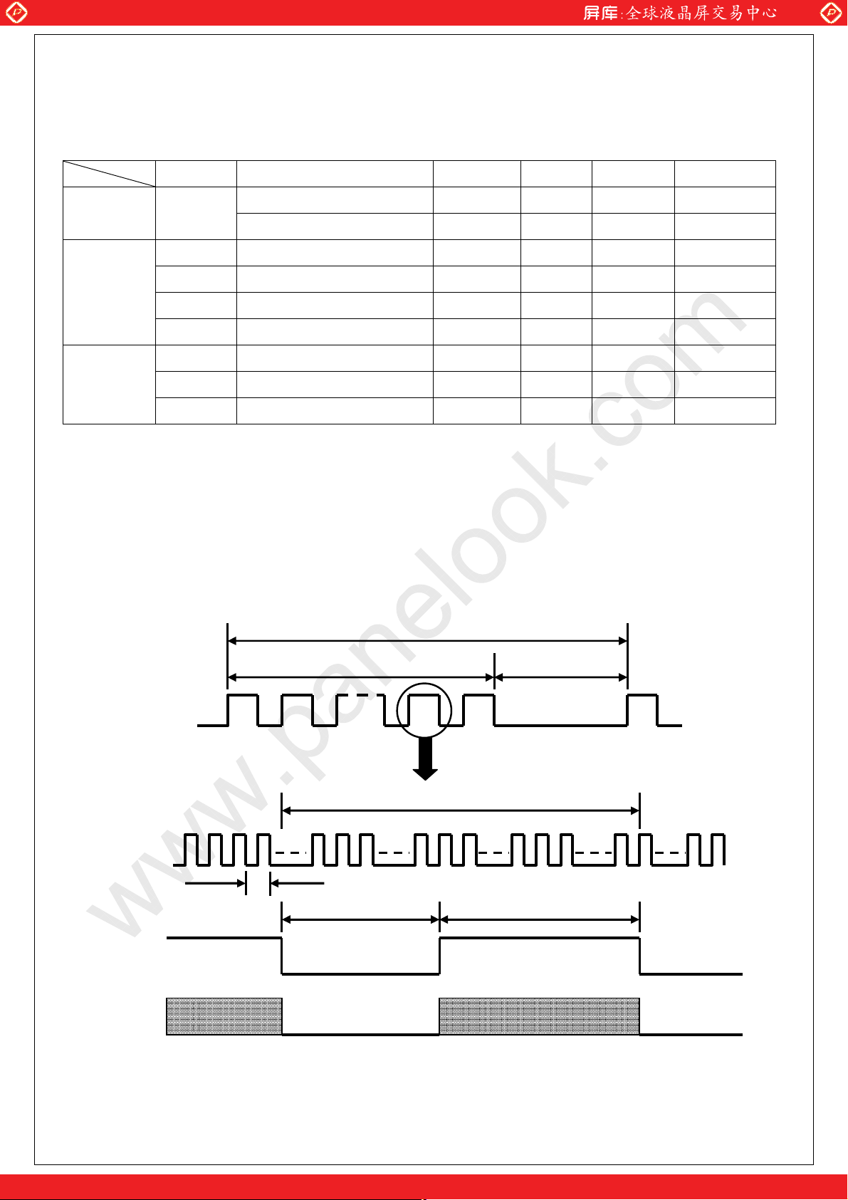
c. Input signal timing
Support Input Timing Table
Item Description Min. Typ. Max. Unit
period 11.63 12.5 20 nS Clock
Dclk
frequency 50 80 86 MHz
Vertica l
Horizontal
T
V_TOTAL
T
T
H_TOTAL
T
V total line number 776 810 1015 T
Data duration
V_DATA
768
Ё
Ё
TVB V-blank 8 42 247 T
frequency 47 60 63 Hz
f
V
H_TOTAL
T
H_TOTAL
H_TOTAL
H total pixel number 1503 1648 2000 DClk
Ё
Data duration
H_DATA
T
H-blank 137 282 634 DClk
HB
1366
Ё
DClk
Note: Because this module is operated by DE only mode, Hsync and Vsync input signals should be set
to low Logic level or ground. Otherwise, this module would operate abnormally.
INPUT SIGNAL TIMING DIAGRAM
Tv
Tvd Tvb
DE
DCLK
Tc
Thb Thd
DE
DATA
One step solution for LCD / PDP / OLED panel application: Datasheet, inventory and accessory!
www.panelook.com
Page 14

Global LCD Panel Exchange Center
www.panelook.com
d. Display Position
D(1, 1) D(2, 1) …… D(683, 1) …… D(1365, 1) D(1366, 1)
D(1, 2) D(2, 2) …… D(683, 2) …… D(1365, 2) D(1366, 2)
.
.
.
D(1, 384) D(2, 384) …… D(683, 384) …… D(1365, 384) D(1366, 384)
.
.
.
D(1, 767) D(2, 767) …… D(683, 767) …… D(1365, 767) D(1366, 767)
D(1, 768) D(2, 768) …… D(683, 768) …… D(1365, 768) D(1366, 768)
……
……
SPEC NO.
PAGE
.
.
.
.
.
.
……
……
TM315GW01 V.0
14/22
.
.
.
.
.
.
.
.
.
.
.
.
One step solution for LCD / PDP / OLED panel application: Datasheet, inventory and accessory!
www.panelook.com
Page 15

Global LCD Panel Exchange Center
yp
y
y
www.panelook.com
C. Optical specifications
Item Symbol Condition
G to G Response time
with INL’s Module
Contrast ratio
with INL’s Module
Bottom
Viewing angle
with INL’s Module
Tγ
CR
Top
Left
θ
= 0ш
θ
= 0ш
CR
CR
CR
Њ10
Њ10
Њ10
SPEC NO.
PAGE
Specification
Min. T
- 8.5 14
2400 3000 -
- 89 -
- 89 -
- 89 -
. Max.
TM315GW01 V.0
15/22
Unit Remark
ms Note 2
Note 1,3
deg. Note 1,3,5
Cell Transparency (%)
with INL’s Module
Color chromaticity(CIE)
With C-Light
White uniformity (9 points)
with INL’s Module
Cross talk
with INL’s Module
Њ10
Right
Tr
CR
Center
Wx
W
Rx
R
θ
Gx
= 0ш
Gy
Bx
By
δ
W
Ct
- 89 -
- 4.62 -
0.317
0.338
0.647
0.337
-0.03
- - 1.3
- - 2%
0.292
0.600
0.138
0.091
+0.03
% Note 1,4
Note 0
Note 1,6
Note 7
Note 0 : Light source is the standard light source “C” which is defined by CIE and driving voltages are
based on suitable gamma voltages. The calculating method is as following
Κ
1. Measure Module’s and BLU’s spectrums. White is without signal input and R, G, B are with
signal input BLU is supplied by INL.
2. Calculate cell’s spectrum.
3. Calculate cell’s chromaticity by using the spectrum of standard light source “C”
One step solution for LCD / PDP / OLED panel application: Datasheet, inventory and accessory!
www.panelook.com
Page 16

Global LCD Panel Exchange Center
igh
(
P1~P9)
g
www.panelook.com
Note 1: 1. Ambient temperature = 25°C.
2. To be measured in dark room after backlight warm up 30 minutes.
3. To be measured with a viewing cone of 2°by Topcon luminance meter BM-5A.
Note 2: G to G Response Time:
Response time Tγ is the average time required for display transition by switching the input
signal for six luminance ratio (0%,20%,40%,60%,80%,100% brightness matrix) and is
based
on fv=60Hz to optimize.
˃ʸ ˃ʸˀ˅˃ʸ ˃ʸˀˇ˃ʸ ˃ʸˀˉ˃ʸ ˃ʸˀˋ˃ʸ ˃ʸˀ˄˃ ˃ʸ
˅˃ʸ ˅˃ʸˀ˃ʸ ˅˃ʸˀˇ˃ʸ ˅˃ʸˀˉ˃ʸ ˅˃ʸˀˋ˃ʸ ˅˃ʸˀ˄˃˃ʸ
ˇ˃ʸ ˇ˃ʸˀ˃ʸ ˇ˃ʸˀ˅˃ʸ ˇ˃ʸˀˉ˃ʸ ˇ˃ʸˀˋ˃ʸ ˇ˃ʸˀ˄˃˃ʸ
ˉ˃ʸ ˉ˃ʸˀ˃ʸ ˉ˃ʸˀ˅˃ʸ ˉ˃ʸˀˇ˃ʸ ˉ˃ʸˀˋ˃ʸ ˉ˃ʸˀ˄˃˃ʸ
ˋ˃ʸ ˋ˃ʸˀ˃ʸ ˋ˃ʸˀ˅˃ʸ ˋ˃ʸˀˇ˃ʸ ˋ˃ʸˀˉ˃ʸ ˋ˃ʸˀ˄˃˃ʸ
˄˃˃ʸ ˄˃˃ʸˀ˃ʸ ˄˃˃ʸˀ˅˃ʸ ˄˃ ˃ʸˀˇ˃ʸ ˄˃˃ʸˀˉ˃ʸ ˄˃˃ʸˀˋ˃ʸ
˃ʸ ˅˃ʸ ˇ˃ʸ ˉ˃ʸ ˋ˃ʸ ˄˃˃ʸ
SPEC NO.
PAGE
TM315GW01 V.0
16/22
Note 3: Definition of contrast ratio:
Contrast ratio is calculated by the following formula.
Contrast ratio (CR)=
Note 4: Driving conditions for CCFL: I
Note 5: Definition of viewing angle
Brightness on the "white" state
Brightness on the "black" state
= 12 mA, 50 KHz Frequency.
L
Note 6: Definition white uniformity:
Luminance are measured at the following nine points (P1~P9).
Ӭ
Minimum Br
!
=
Maximum Bri
tness of ninepoints
htness of ninepoints (P1~P9).
.
One step solution for LCD / PDP / OLED panel application: Datasheet, inventory and accessory!
www.panelook.com
Page 17

Global LCD Panel Exchange Center
www.panelook.com
Note 7:
SPEC NO.
1/2
1/6
PAGE
2/3 1/3
A
1/6
A’
127 gray level 127 gray level
B
1/2
1/2
TM315GW01 V.0
17/22
1/6
1/6
1/3
1/2
B’
2/3
l L
l L
l / LA x 100%= 2% max., LA and LA’ are brightness at location A and A’
A-LA’
l / LB x 100%= 2% max., LB and LB’ are brightness at location B and B’
B-LB’
Note 10: Optical characteristic measurement setup.
255 gray level
One step solution for LCD / PDP / OLED panel application: Datasheet, inventory and accessory!
www.panelook.com
Page 18

Global LCD Panel Exchange Center
www.panelook.com
SPEC NO.
PAGE
TM315GW01 V.0
18/22
E. Safety
(1) Sharp Edge Requirements
There will be no sharp edges or corners on the display assembly that could cause injury.
(2) Materials
a. Toxicity
There will be no carcinogenic materials used anywhere in the display module. If toxic materials
are used, they will be reviewed and approved by the responsible InnoLux Toxicologist.
b. Flammability
All components including electrical components that do not meet the flammability grade UL94-V1
in the module will complete the flammability rating exception approval process. The printed circuit
board will be made from material rated 94-V1 or better. The actual UL flammability rating will be
printed on the printed circuit board.
c. Capacitors
If any polarized capacitors are used in the display assembly, provisions will be made to keep them
from being inserted backwards.
F. Display quality
The display quality of the color TFT-LCD module should be in compliance with the
Innolux’s Incoming inspection standard.
G. Handling precaution
The Handling of the TFT-LCD should be in compliance with the Innolux’s handling principle
standard.
One step solution for LCD / PDP / OLED panel application: Datasheet, inventory and accessory!
www.panelook.com
Page 19

Global LCD Panel Exchange Center
www.panelook.com
H. Label
(1) Module Label
SPEC NO.
PAGE
TM315GW01 V.0
19/22
(a) Model Name: V320BJ5-P01
(b) Revision: Rev. XX, for example: A0, A1… B1, B2… or C1, C2…etc.
(c)
Serial ID includes the information as below:
(a) Manufactured Date: Year: 0~9, for 2010~2019
Month: 1~9, A~C, for Jan. ~ Dec.
Day: 1~9, A~Y, for 1
(b) Revision Code: Cover all the change
(c) Serial No.: Manufacturing sequence of product
st
to 31st, exclude I ,O, and U.
(d) Product Line: 1 -> Line1, 2 -> Line 2, …etc.
One step solution for LCD / PDP / OLED panel application: Datasheet, inventory and accessory!
www.panelook.com
Page 20

Global LCD Panel Exchange Center
www.panelook.com
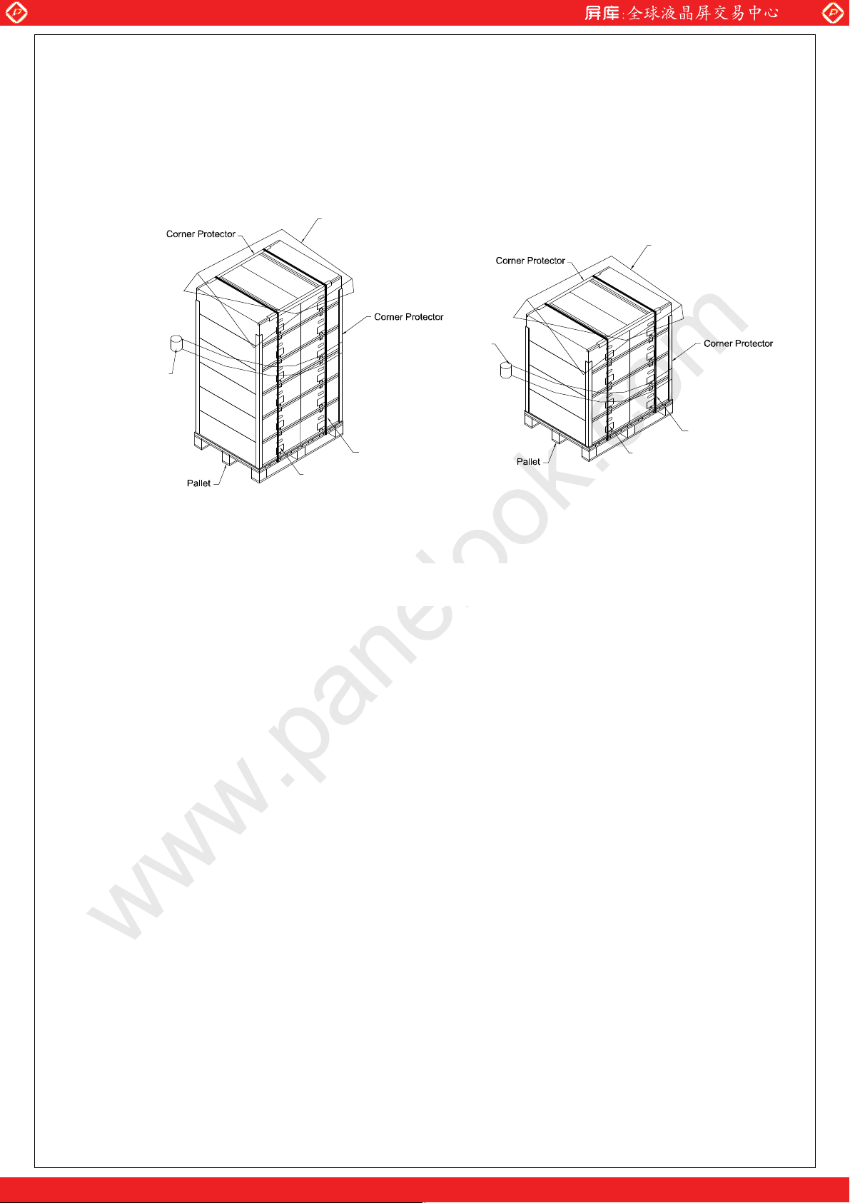
I. Packing specification
1. PACKAGING
1.1 PACKING SPECIFICATIONS
(1) 21 LCD TV Panels / 1 Box
(2) Box dimensions : 970 (L) X 640 (W) X 319 (H)
(3) Weight : approximately 38Kg ( 21 panels per box)
1.2 PACKING METHOD
Figures I-1 and I-2 are the packing method
panel
SPEC NO.
PAGE
Top layer for empty tray
Tray need to revolve stack
TM315GW01 V.0
20/22
Tape
Cushion(EPE Board )
PP Board
Bag
Carton Label
Carton
Figure.I-1 packing method
One step solution for LCD / PDP / OLED panel application: Datasheet, inventory and accessory!
www.panelook.com
Page 21
Global LCD Panel Exchange Center
www.panelook.com
SPEC NO.
PAGE
TM315GW01 V.0
21/22
Sea & Land Transportation
PE Sheet
(L1000*50*50mm)
(L1850*50*50mm)
Film
Film
PP Belt
Carton Label
(L1300*W1000*H140mm)
Air Transportation
PE Sheet
(L1000*50*50mm)
(L1130*50*50mm)
PP Belt
Carton Label
(L1300*W1000*H140mm)
Figure.I-2 packing method
One step solution for LCD / PDP / OLED panel application: Datasheet, inventory and accessory!
www.panelook.com
Page 22

www.panelook.com
TM315GW01 V.0
22/22
www.panelook.com
SPEC NO.
PAGE
Global LCD Panel Exchange Center
One step solution for LCD / PDP / OLED panel application: Datasheet, inventory and accessory!
J. Mechanical drawing
Page 23

www.panelook.com
TM315GW01 V.0
23/22
www.panelook.com
SPEC NO.
PAGE
Global LCD Panel Exchange Center
One step solution for LCD / PDP / OLED panel application: Datasheet, inventory and accessory!
 Loading...