

Page 1
Global LCD Panel Exchange Center
MODEL NO.: N156BGE
www.panelook.com
PRODUCT SPECIFICATION
Doc. Number:
ϭʳ Tentative Specification
ϭʳ Preliminary Specification
Ϯʳ Approval Specification
SUFFIX: L21
Customer: Lenovo International
APPROVED BY SIGNATURE
Note
Please return 1 copy for your confirmation with your
signature and comments.
Approved By Checked By Prepared By
ᄘ࿚ໃ
2011-01-27
09:59:36 CST
ຫၝᎮ
2011-01-10
08:06:02 CST
׆ි
2010-12-21
17:18:30 CST
Version 3.0 27 January 2011 1 / 37
The copyright belongs to CHIMEI InnoLux. Any unauthorized use is prohibited.
One step solution for LCD / PDP / OLED panel application: Datasheet, inventory and accessory!
www.panelook.com
Page 2
Global LCD Panel Exchange Center
www.panelook.com
PRODUCT SPECIFICATION
CONTENTS
1. GENERAL DESCRIPTION .........................................................................................................4
1.1 OVERVIEW ................................................................................................................................4
1.2 GENERAL SPECIFICATI0NS ...................................................................................................4
2. MECHANICAL SPECIFICATIONS ............................................................................................. 4
2.1 CONNECTOR TYPE.................................................................................................................. 4
3. ABSOLUTE MAXIMUM RATINGS .............................................................................................4
3.1 ABSOLUTE RATINGS OF ENVIRONMENT ..........................................................................5
3.2 ELECTRICAL ABSOLUTE RATINGS...................................................................................... 5
3.2.1 TFT LCD MODULE ............................................................................................................5
4. ELECTRICAL SPECIFICATIONS............................................................................................... 6
4.1 FUNCTION BLOCK DIAGRAM............................................................................................... 6
4.2. INTERFACE CONNECTIONS .................................................................................................6
4.3 ELECTRICAL CHARACTERISTICS........................................................................................ 8
4.3.1 LCD ELETRONICS SPECIFICATION ...............................................................................8
4.3.2 LED CONVERTER SPECIFICATION..............................................................................10
4.3.3 BACKLIGHT UNIT...........................................................................................................12
4.4 LVDS INPUT SIGNAL TIMING SPECIFICATIONS .............................................................13
4.4.1 LVDS DC SPECIFICATIONS ...........................................................................................13
4.4.2 LVDS DATA FORMAT ......................................................................................................13
4.4.3 COLOR DATA INPUT ASSIGNMENT ............................................................................14
4.5 DISPLAY TIMING SPECIFICATIONS ...................................................................................15
4.6 POWER ON/OFF SEQUENCE ................................................................................................16
5. OPTICAL CHARACTERISTICS ............................................................................................... 17
5.1 TEST CONDITIONS................................................................................................................. 17
5.2 OPTICAL SPECIFICATIONS ..................................................................................................17
6. RELIABILITY TEST ITEM ......................................................................................................201
7. PACKING................................................................................................................................222
7.1 MODULE LABEL ..................................................................................................................222
7.2 CARTON ................................................................................................................................. 244
7.3 PALLET................................................................................................................................... 255
8. PRECAUTIONS ...................................................................................................................... 266
8.1 HANDLING PRECAUTIONS................................................................................................ 266
8.2 STORAGE PRECAUTIONS ..................................................................................................266
8.3 OPERATION PRECAUTIONS...............................................................................................266
Appendix. EDID DATA STRUCTURE.........................................................................................277
Appendix. OUTLINE DRAWING .................................................................................................. 30
Version 3.0 27 January 2011 2 / 37
The copyright belongs to CHIMEI InnoLux. Any unauthorized use is prohibited.
One step solution for LCD / PDP / OLED panel application: Datasheet, inventory and accessory!
www.panelook.com
Page 3
Global LCD Panel Exchange Center
REVISION HISTORY
Version Date Page Description
1.0 Aug.20, 2010 All Spec Ver.1.0 was first issued.
3.0 Oct.02, 2010 All Spec Ver.3.0 was first issued.
www.panelook.com
PRODUCT SPECIFICATION
Version 3.0 27 January 2011 3 / 37
The copyright belongs to CHIMEI InnoLux. Any unauthorized use is prohibited.
One step solution for LCD / PDP / OLED panel application: Datasheet, inventory and accessory!
www.panelook.com
Page 4
Global LCD Panel Exchange Center
1. GENERAL DESCRIPTION
1.1 OVERVIEW
N156BGE-L21 is a 15.6” (15.547” diagonal) TFT Liquid Crystal Display module with LED Backlight
unit and 40 pins LVDS interface. This module supports 1366 x 768 HD mode and can display
262,144 colors. The optimum viewing angle is at 6 o’clock direction.
1.2 GENERAL SPECIFICATI0NS
Item Specification Unit Note
Screen Size 15.547 diagonal
Driver Element a-si TFT active matrix - Pixel Number 1366 x R.G.B. x 768 pixel Pixel Pitch 0.252 (H) x 0.252 (V) mm Pixel Arrangement RGB vertical stripe - Display Colors 262,144 color Transmissive Mode Normally white - Surface Treatment Hard coating (3H), Glare - Luminance, White 220 Cd/m2
Power Consumption Total 5.184 W (Max.) @ cell 0.9 W (Max.), BL 4.284W (Max.) (1)
Note (1) The specified power consumption (with converter efficiency) is under the conditions at VCCS =
www.panelook.com
PRODUCT SPECIFICATION
3.3 V, fv = 60 Hz, LED_VCCS = Typ, fPWM = 200 Hz, Duty=100% and Ta = 25 ± 2 ºC, whereas mosaic
pattern is displayed.
2. MECHANICAL SPECIFICATIONS
Item Min. Typ. Max. Unit Note
Horizontal (H) 358.8 359.3 359.8 mm
Module Size
Bezel Area
Active Area
Note (1) Please refer to the attached drawings for more information of front and back outline dimensions.
Vertical (V) 209 209.5 210 mm
Thickness (T) - 5.2 5.5 mm
Horizontal 349.28 349.58 349.88 mm
Vertical 197.99 198.29 198.59 mm
Horizontal - 344.232 - mm
Vertical - 193.536 - mm
Weight - 430 445 g
2.1 CONNECTOR TYPE
Pin1 Pin40
(1)
Please refer Appendix Outline Drawing for detail design.
Connector Part No.: IPEX-20455-040E-12 or Tyco 5-2069716-3
User’s connector Part No: IPEX-20453-040T-01
Version 3.0 27 January 2011 4 / 37
The copyright belongs to CHIMEI InnoLux. Any unauthorized use is prohibited.
One step solution for LCD / PDP / OLED panel application: Datasheet, inventory and accessory!
www.panelook.com
Page 5
Global LCD Panel Exchange Center
3. ABSOLUTE MAXIMUM RATINGS
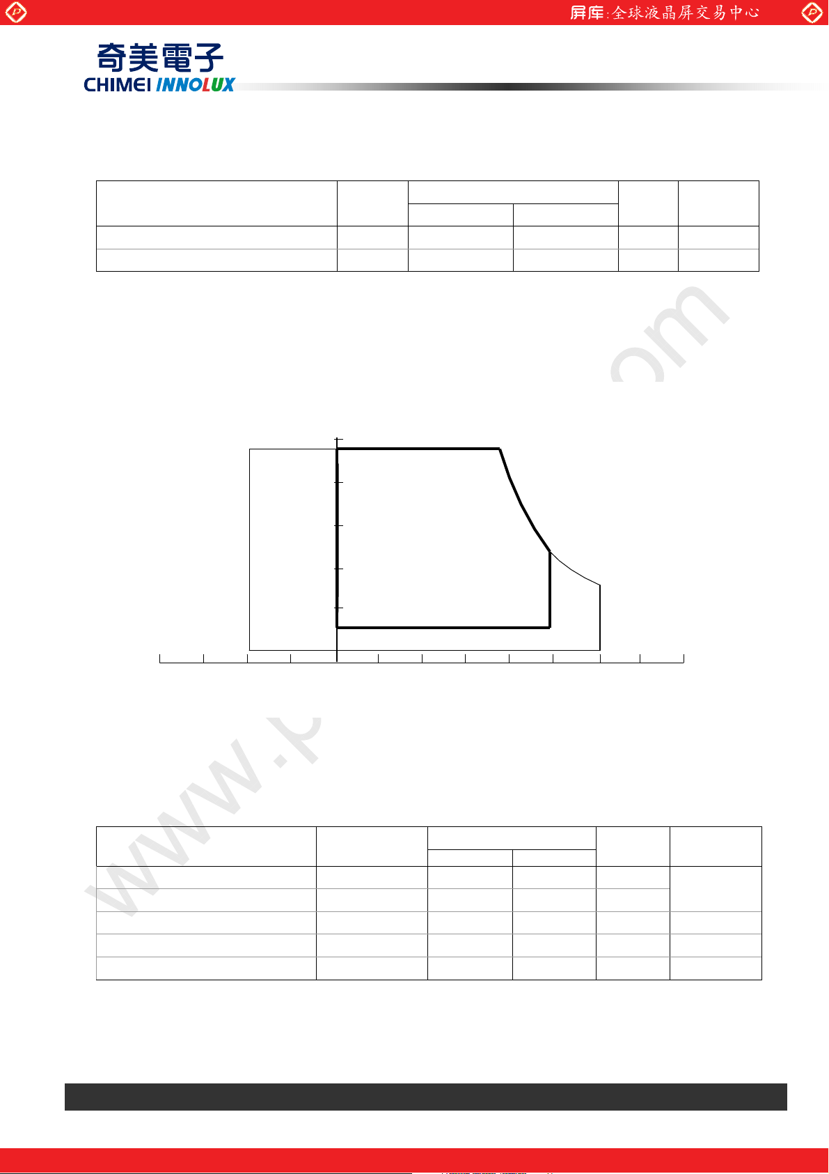
3.1 ABSOLUTE RATINGS OF ENVIRONMENT
Item Symbol
Storage Temperature TST -20 +60 ºC (1)
Operating Ambient Temperature TOP 0 +50 ºC (1), (2)
Note (1) (a) 90 %RH Max. (Ta <= 40 ºC).
(b) Wet-bulb temperature should be 39 ºC Max. (Ta > 40 ºC).
(c) No condensation.
Note (2) The temperature of panel surface should be 0 ºC min. and 60 ºC max.
Relative Humidity (%RH)
100
95
www.panelook.com
PRODUCT SPECIFICATION
Value
Min. Max.
Unit Note
80
60
40
20
8
5
Operating
S
Temperature (ºC)
3.2 ELECTRICAL ABSOLUTE RATINGS
3.2.1 TFT LCD MODULE
Item Symbol
Power Supply Voltage VCCS -0.3 +4.0 V
Logic Input Voltage VIN -0.3 VCCS+0.3 V
Converter Input Voltage
Converter Control Signal Voltage
Converter Control Signal Voltage
LED_VCCS
LED_PWM,
LED_EN
Value
Min. Max.
-0.3 24 V (1)
-0.3 5 V (1)
-0.3 5 V (1)
Unit Note
8060-20 40 0 20 -40
(1)
Note (1) Stresses beyond those listed in above “ELECTRICAL ABSOLUTE RATINGS” may cause
permanent damage to the device. Normal operation should be restricted to the conditions
described in “ELECTRICAL CHARACTERISTICS”.
Version 3.0 27 January 2011 5 / 37
The copyright belongs to CHIMEI InnoLux. Any unauthorized use is prohibited.
One step solution for LCD / PDP / OLED panel application: Datasheet, inventory and accessory!
www.panelook.com
Page 6
Global LCD Panel Exchange Center
4. ELECTRICAL SPECIFICATIONS
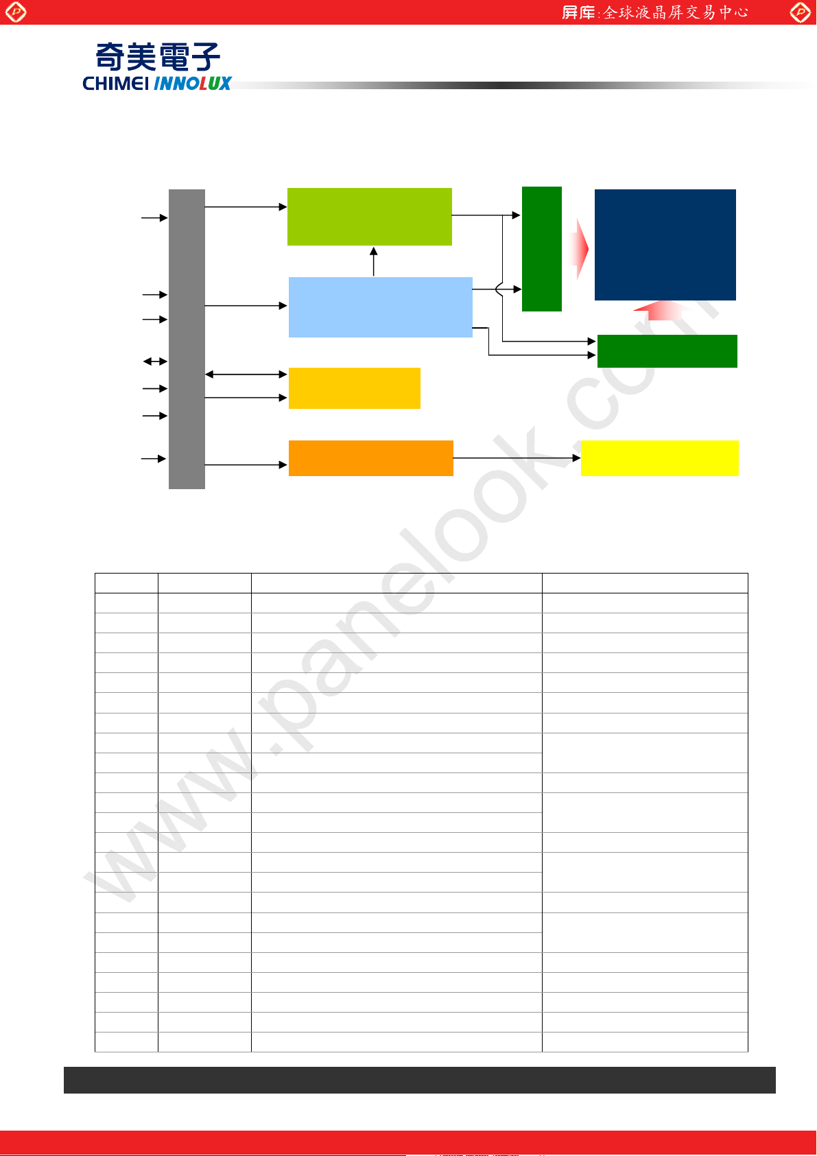
4.1 FUNCTION BLOCK DIAGRAM
LVDS Display
Data & Clock
VCCS
GND
Data
EDID
CLK
EDID
V
EDID
INPUT CONNECTOR
www.panelook.com
PRODUCT SPECIFICATION
SCAN DRIVER IC
TIMING ONTROLLER
TFT LCD
PANEL
DC/DC CONVERTER &
REFERENCE VOLTAGE
GENERATOR
DATA DRIVER IC
EDID
EEPROM
Converter
Input Signals
4.2. INTERFACE CONNECTIONS
PIN ASSIGNMENT
Pin Symbol Description Remark
1 NC No Connection (Reserve)
2 VCCS Power Supply (3.3V typ.)
3 VCCS Power Supply (3.3V typ.)
4 VEDID DDC 3.3V power
5 NC No Connection (Reserved for CMI test)
6 CLKEDID DDC clock
7 DATAEDID DDC data
8 Rxin0- LVDS differential data input
9 Rxin0+ LVDS differential data input
10 VSS Ground
11 Rxin1- LVDS differential data input
12 Rxin1+ LVDS differential data input
13 VSS Ground
14 Rxin2- LVDS Differential Data Input
15 Rxin2+ LVDS Differential Data Input
16 VSS Ground
17 RxCLK- LVDS differential clock input
18 RxCLK+ LVDS differential clock input
19 VSS Ground
20 NC No Connection (Reserve)
21 NC No Connection (Reserve)
22 VSS Ground
23 NC No Connection (Reserve)
LED CONVERTER BACKLIGHT UNIT
R0-R5, G0
G1~G5, B0, B1
B2-B5,HS,VS, DE
LVDS CL K
Version 3.0 27 January 2011 6 / 37
The copyright belongs to CHIMEI InnoLux. Any unauthorized use is prohibited.
One step solution for LCD / PDP / OLED panel application: Datasheet, inventory and accessory!
www.panelook.com
Page 7
Global LCD Panel Exchange Center
24 NC No Connection (Reserve)
25 VSS Ground
26 NC No Connection (Reserve)
27 NC No Connection (Reserve)
28 VSS Ground
29 NC No Connection (Reserve)
30 NC No Connection (Reserve)
31 LED_GND LED Ground
32 LED_GND LED Ground
33 LED_GND LED Ground
34 NC No Connection (Reserve)
35 LED_PWM PWM Control Signal of LED Converter
36 LED_EN Enable Control Signal of LED Converter
37 NC No Connection (Reserve)
38 LED_VCCS LED Power Supply
39 LED_VCCS LED Power Supply
40 LED_VCCS LED Power Supply
www.panelook.com
PRODUCT SPECIFICATION
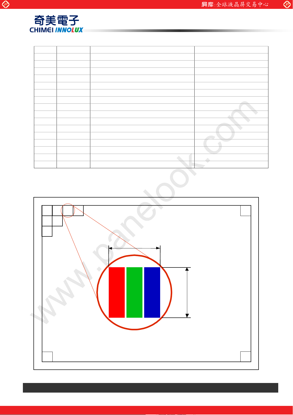
Note (1) The first pixel is odd as shown in the following figure.
1,1
(odd)
2,1
1,2
(even)
2,2
1,3
(odd)
1,4
(even)
3,1
Pitch
1,Xmax
Pitch
Ymax,1
Version 3.0 27 January 2011 7 / 37
The copyright belongs to CHIMEI InnoLux. Any unauthorized use is prohibited.
One step solution for LCD / PDP / OLED panel application: Datasheet, inventory and accessory!
Ymax,
Xmax
www.panelook.com
Page 8
Global LCD Panel Exchange Center
4.3 ELECTRICAL CHARACTERISTICS
4.3.1 LCD ELETRONICS SPECIFICATION
Parameter Symbol
Power Supply Voltage VCCS 3.0 3.3 3.6 V (1)-
Ripple Voltage VRP - 50 - mV (1)-
www.panelook.com
PRODUCT SPECIFICATION
Value
Unit Note
Min. Typ. Max.
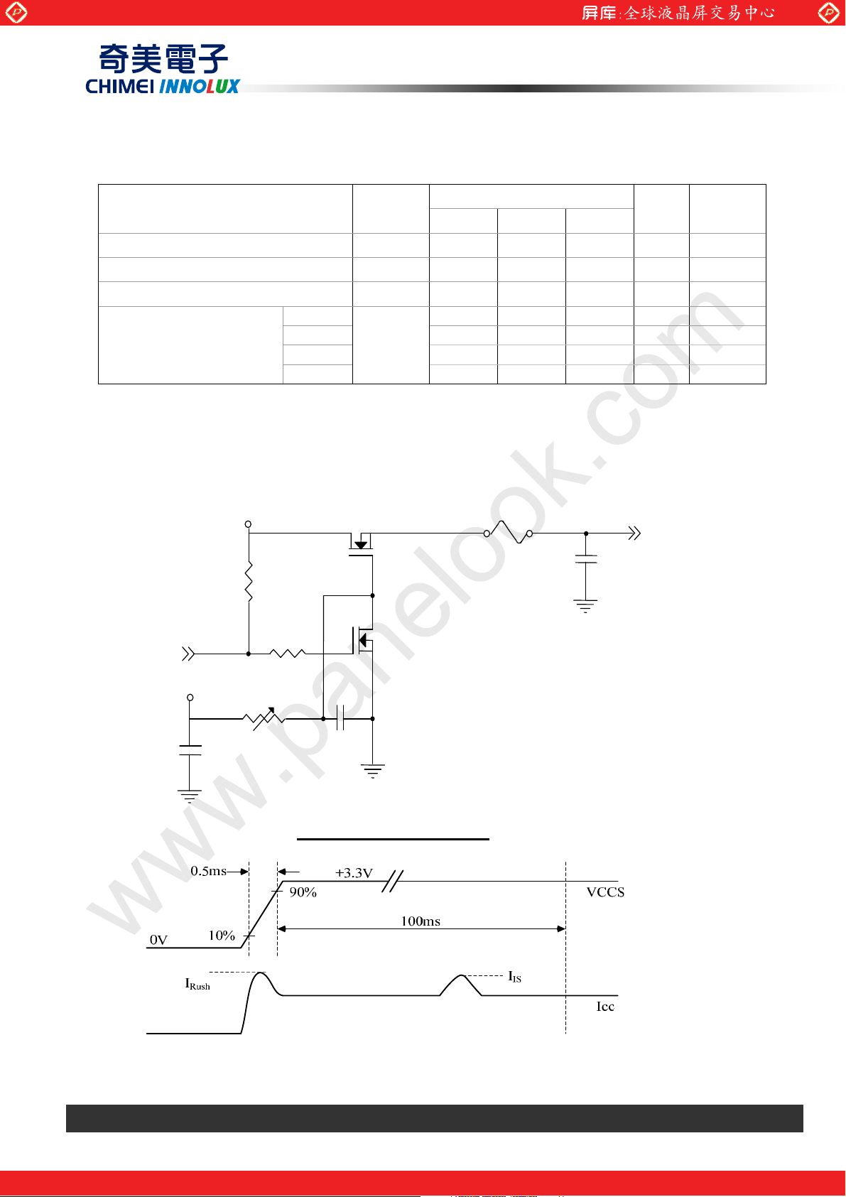
Inrush Current I
Mosaic
Power Supply Current
Black
Win XP
1H2V
- - 1.5 A (1),(2)
RUSH
lcc
ˀ
ˀ
ˀ
260 270 mA (3)a
320 350 mA (3)b
265 290 mA
- 310 340 mA
Note (1) The ambient temperature is Ta = 25 ± 2 ºC.
Note (2) I
: the maximum current when VCCS is rising
RUSH
I
: the maximum current of the first 100ms after power-on
IS
Measurement Conditions: Shown as the following figure. Test pattern: black.
+3.3V
Q1 2SK1475
R1
47K
FUSE
C3
1uF
(High to Low)
(Control Signal)
SW
+12V
C1
1uF
VR1
R2
1K
47K
0.01uF
Q2
2SK1470
C2
VCCS
(LCD Module Input)
VCCS rising time is 0.5ms
Version 3.0 27 January 2011 8 / 37
The copyright belongs to CHIMEI InnoLux. Any unauthorized use is prohibited.
One step solution for LCD / PDP / OLED panel application: Datasheet, inventory and accessory!
www.panelook.com
Page 9
Global LCD Panel Exchange Center
Note (3) The specified power supply current is under the conditions at VCCS = 3.3 V, Ta = 25 ± 2 ºC, DC
www.panelook.com
PRODUCT SPECIFICATION
Current and f
a. Mosaic Pattern
= 60 Hz, whereas a power dissipation check pattern below is displayed.
v
b. Black Pattern
Active Area
Active Area
Version 3.0 27 January 2011 9 / 37
The copyright belongs to CHIMEI InnoLux. Any unauthorized use is prohibited.
One step solution for LCD / PDP / OLED panel application: Datasheet, inventory and accessory!
www.panelook.com
Page 10
Global LCD Panel Exchange Center
4.3.2 LED CONVERTER SPECIFICATION
Parameter Symbol
www.panelook.com
PRODUCT SPECIFICATION
Value
Unit Note
Min. Typ. Max.
Converter Input power supply voltage
Converter Inrush Current
LED_Vccs
ILED
RUSH
6.0 12.0 21.0 V
- - 1.5 A (1)
Backlight On 2.0 - 5 V
EN Control Level
Backlight Off
0 - 0.5 V
PWM High Level 2.3 - 5 V
PWM Control Level
PWM Low Level
0 - 0.5 V
10 - 100 %
PWM Control Duty Ratio
1 - 100 % (2)
PWM Control Permissive Ripple
Voltage
PWM Control Frequency f
VPWM_pp
100 - 2K Hz (3)
PWM
- - 100 mV
LED Power Current LED_VCCS =Typ. ILED 288 339 398 mA (4)
Note (1) ILED
ILED
: the maximum current when LED_VCCS is rising,
RUSH
: the maximum current of the first 100ms after power-on,
IS
Measurement Conditions: Shown as the following figure. LED_VCCS = Typ, Ta = 25 ± 2 ºC, f
= 200 Hz, Duty=100%.
PWM
LED_VCCS(Typ)
Q1 IRL3303
VR1
R1
47K
47K
R2
1K
0.01uF
Q2
IRL3303
C2
(High to Low)
(Control Signal)
SW=24V
LED_VCCS(Typ)
C1
1uF
FUSE
C3
1uF
(LED Converter Input)
Version 3.0 27 January 2011 10 / 37
The copyright belongs to CHIMEI InnoLux. Any unauthorized use is prohibited.
One step solution for LCD / PDP / OLED panel application: Datasheet, inventory and accessory!
www.panelook.com
Page 11
Global LCD Panel Exchange Center
www.panelook.com
PRODUCT SPECIFICATION
LED_VCC
LED_PWM
LED_EN
ILED
0V
0V
0V
ILED
VLED rising time is 0.5ms
0.5ms
90%
10%
Rush
100ms
ILED
IS
Note (2) If the PWM control duty ratio is less than 10%, it is difficult to control the brightness linearity
Note (3) If PWM control frequency is applied in the range less than 1KHz, the “waterfall” phenomenon on
the screen may be found. To avoid the issue, it’s a suggestion that PWM control frequency should
follow the criterion as below.
PWM control frequency f
d fN )33.0( f
should be in the range
PWM
fN d )66.0(
PWM
N : Integer )3( tN
f : Frame rate
Note (4) The specified LED power supply current is under the conditions at “LED_VCCS = Typ.”, Ta = 25
± 2 ºC, f
Note (5) Within the specified PWM control duty ratio range, CMI’s LCD module can pass the following
acoustic noise test. The test condition refers to ISO-7779 and is shown as the following figure.
= 200 Hz, Duty=100%.
PWM
LED_VCCS = Min., Ta = 25 ± 2 ºC, (D
while operating on black pattern with CMI’s own pattern generator. All sound pressure of scanning
band 630Hz - 20KHz should be kept under 20dBA. If lower noise level is required, more technical
discussion is needed.
PWM, fPWM) = (Max, Max); (Max, Min); (Min, Max); (Min, Min),
Version 3.0 27 January 2011 11 / 37
The copyright belongs to CHIMEI InnoLux. Any unauthorized use is prohibited.
One step solution for LCD / PDP / OLED panel application: Datasheet, inventory and accessory!
www.panelook.com
Page 12
Global LCD Panel Exchange Center
www.panelook.com
PRODUCT SPECIFICATION
4.3.3 BACKLIGHT UNIT
Ta = 25 ± 2 ºC
Parameter Symbol
LED Light Bar Power
Supply Voltage
LED Light Bar Power
Supply Current
Power Consumption PL 2.554 3.072 3.472 W (3)
LED Life Time LBL 15000 - - Hrs (4)
Note (1) LED current is measured by utilizing a high frequency current meter as shown below :
Light Bar Feedback
Channels
L 22.4 25.6 27.2 V
V
L 114 120 126 mA
I
Min. Typ. Max.
V
L, IL
Value
LED
Light Bar
Unit Note
(1)(2)(Duty100%)
Note (2) For better LED light bar driving quality, it is recommended to utilize the adaptive boost converter
with current balancing function to drive LED light-bar.
Note (3) P
Note (4) The lifetime of LED is defined as the time when it continues to operate under the conditions at Ta =
25 ±2
= IL ×VL (Without LED converter transfer efficiency)
L
o
C and IL = 24 mA(Per EA) until the brightness becomes 50% of its original value.Љ
Version 3.0 27 January 2011 12 / 37
The copyright belongs to CHIMEI InnoLux. Any unauthorized use is prohibited.
One step solution for LCD / PDP / OLED panel application: Datasheet, inventory and accessory!
www.panelook.com
Page 13

Global LCD Panel Exchange Center
|
|
www.panelook.com
PRODUCT SPECIFICATION
4.4 LVDS INPUT SIGNAL TIMING SPECIFICATIONS
4.4.1 LVDS DC SPECIFICATIONS
Parameter Symbol
Min. Typ. Max.
LVDS Differential Input High Threshold V
LVDS Differential Input Low Threshold V
LVDS Common Mode Voltage VCM 1.125 - 1.375 V (1)
LVDS Differential Input Voltage |VID| 100 - 600 mV (1)
LVDS Terminating Resistor RT - 100 - Ohm -
Note (1) The parameters of LVDS signals are defined as the following figures.
Single Ended
V
0V
CM
TH(LVDS)
-100 - - mV
TL(LVDS)
- - +100 mV
Value
Unit Note
V
CM
V
CM
VID|
(1),
=1.2V
(1)
=1.2V
Differential
4.4.2 LVDS DATA FORMAT
CLK+
Rxin2
Rxin1
Rxin0
T/7
IN20 IN19 IN18 IN17 IN16 IN15 IN14
DE B5 B4 B3 B2 Vsync Hsync
IN13 IN12 IN11 IN10 IN9 IN8 IN7
B1 G4 G3 G2 G1 B0 G5
IN6
G0 R3 R2 R1 R0
V
0V
V
IN5 IN4 IN3 IN2 IN1 IN0
R5
VID|
R4
Signal for 1 DCLK Cycle (T)
Version 3.0 27 January 2011 13 / 37
The copyright belongs to CHIMEI InnoLux. Any unauthorized use is prohibited.
One step solution for LCD / PDP / OLED panel application: Datasheet, inventory and accessory!
www.panelook.com
Page 14

Global LCD Panel Exchange Center
4.4.3 COLOR DATA INPUT ASSIGNMENT
The brightness of each primary color (red, green and blue) is based on the 6-bit gray scale data input
for the color. The higher the binary input the brighter the color. The table below provides the assignment
of color versus data input.
Color
R5 R4 R3 R2 R1 R0 G5 G4 G3 G2 G1 G0 B5 B4 B3 B2 B1 B0
Black
Red
Green
Basic
Colors
Gray
Scale
Of
Red
Gray
Scale
Of
Green
Gray
Scale
Of
Blue
Note (1) 0: Low Level Voltage, 1: High Level Voltage
Blue
Cyan
Magenta
Yellow
White
Red(0)/Dark
Red(1)
Red(2)
:
:
Red(61)
Red(62)
Red(63)
Green(0)/Dark
Green(1)
Green(2)
:
:
Green(61)
Green(62)
Green(63)
Blue(0)/Dark
Blue(1)
Blue(2)
:
:
Blue(61)
Blue(62)
Blue(63)
0
1
0
0
0
1
1
1
0
0
0
:
:
1
1
1
0
0
0
:
:
0
0
0
0
0
0
:
:
0
0
0
www.panelook.com
PRODUCT SPECIFICATION
Data Signal
Red Green Blue
0
0
0
0
0
0
0
0
0
0
0
0
0
0
0
0
0
1
1
1
1
1
0
0
0
0
0
0
0
0
0
0
0
0
0
0
0
0
0
1
1
1
1
1
1
0
0
0
0
0
0
0
0
0
0
0
0
0
0
0
0
0
1
1
1
1
1
1
0
0
0
0
0
1
1
1
1
1
1
1
1
1
1
1
1
1
1
1
1
1
0
0
0
0
0
0
1
1
1
1
1
1
1
1
1
1
1
1
1
1
1
1
1
0
0
0
0
0
0
1
1
1
1
1
1
1
1
1
1
1
1
1
1
1
1
1
0
0
0
0
0
0
0
0
0
0
0
0
0
0
0
0
0
0
0
0
0
1
0
0
0
0
0
0
0
0
0
0
0
0
0
0
0
1
0
0
0
0
0
0
0
0
0
0
0
0
0
:
:
:
:
:
:
:
:
:
:
:
:
:
:
:
:
:
:
:
:
:
:
:
:
:
:
:
:
:
:
:
:
:
:
1
1
1
0
1
0
0
0
0
0
0
0
0
0
0
0
0
1
1
1
1
0
0
0
0
0
0
0
0
0
0
0
0
0
1
1
1
1
1
0
0
0
0
0
0
0
0
0
0
0
0
0
0
0
0
0
0
0
0
0
0
0
0
0
0
0
0
0
0
0
0
0
0
0
0
0
0
0
1
0
0
0
0
0
0
0
0
0
0
0
0
0
0
0
1
0
0
0
0
0
0
0
:
:
:
:
:
:
:
:
:
:
:
:
:
:
:
:
:
:
:
:
:
:
:
:
:
:
:
:
:
:
:
:
:
:
0
0
0
0
0
1
1
1
1
0
1
0
0
0
0
0
0
0
0
0
0
0
1
1
1
1
1
0
0
0
0
0
0
0
0
0
0
0
0
1
1
1
1
1
1
0
0
0
0
0
0
0
0
0
0
0
0
0
0
0
0
0
0
0
0
0
0
0
0
0
0
0
0
0
0
0
0
0
0
0
0
0
0
0
1
0
0
0
0
0
0
0
0
0
0
0
0
0
0
0
1
0
:
:
:
:
:
:
:
:
:
:
:
:
:
:
:
:
:
:
:
:
:
:
:
:
:
:
:
:
:
:
:
:
:
:
0
0
0
0
0
0
0
0
0
0
0
1
1
1
1
0
1
0
0
0
0
0
0
0
0
0
0
0
1
1
1
1
1
0
0
0
0
0
0
0
0
0
0
0
0
1
1
1
1
1
1
Version 3.0 27 January 2011 14 / 37
The copyright belongs to CHIMEI InnoLux. Any unauthorized use is prohibited.
One step solution for LCD / PDP / OLED panel application: Datasheet, inventory and accessory!
www.panelook.com
Page 15

Global LCD Panel Exchange Center
4.5 DISPLAY TIMING SPECIFICATIONS
The input signal timing specifications are shown as the following table and timing diagram.
Refresh rate 60Hz
Signal Item Symbol Min. Typ. Max. Unit Note
DCLK Frequency 1/Tc 62.4 69.3 72.8 MHz -
Vertical Total Time TV 772 788 793 TH -
Vertical Active Display Period TVD 768 768 768 TH -
DE
Refresh rate 50Hz
Signal Item Symbol Min. Typ. Max. Unit Note
DCLK Frequency 1/Tc 57.418 60.44 63.462 MHz -
DE
Refresh rate 40Hz
Signal Item Symbol Min. Typ. Max. Unit Note
DCLK Frequency 1/Tc 45.93 48.35 50.77 MHz -
DE
Note (1) Because this module is operated by DE only mode, Hsync and Vsync are ignored.
Vertical Active Blanking Period TVB TV-TVD 20 TV-TVD TH -
Horizontal Total Time TH 1456 1466 1492 Tc -
Horizontal Active Display Period THD 1366 1366 1366 Tc -
Horizontal Active Blanking Period THB
Vertical Total Time TV 772 788 793 TH -
Vertical Active Display Period TVD 768 768 768 TH -
Vertical Active Blanking Period TVB TV-TVD 20 TV-TVD TH -
Horizontal Total Time TH 1523 1534 1561 Tc -
Horizontal Active Display Period THD 1366 1366 1366 Tc -
Horizontal Active Blanking Period THB
Vertical Total Time TV 772 788 793 TH -
Vertical Active Display Period TVD 768 768 768 TH -
Vertical Active Blanking Period TVB TV-TVD 20 TV-TVD TH -
Horizontal Total Time TH 1523 1534 1561 Tc -
Horizontal Active Display Period THD 1366 1366 1366 Tc -
Horizontal Active Blanking Period THB
www.panelook.com
PRODUCT SPECIFICATION
TH-THD
TH-THD
TH-THD
100
168
168
TH-THD
TH-THD
TH-THD
Tc -
Tc -
Tc -
INPUT SIGNAL TIMING DIAGRAM
DE
DCLK
DE
DATA
TC
HD
T
Version 3.0 27 January 2011 15 / 37
The copyright belongs to CHIMEI InnoLux. Any unauthorized use is prohibited.
One step solution for LCD / PDP / OLED panel application: Datasheet, inventory and accessory!
www.panelook.com
Page 16

Global LCD Panel Exchange Center
4.6 POWER ON/OFF SEQUENCE
The power sequence specifications are shown as the following table and diagram.
Symbol
t1 0.5 - 10 ms
t2 0 - 50 ms
t3 0 - - ms
t4 150 - - ms
t5 200 - - ms
t6 0 - - ms
t7 0 - 10 ms
tA 0.5 - 10 ms
t
B
tC 0 - - ms
tD 0 - - ms
tE 0 - - ms
tF 0 - - ms
Min. Typ. Max.
0
Value
www.panelook.com
PRODUCT SPECIFICATION
Unit Note
ˀ
ms
- Power Supply
for LCD, VCCS
- Interface Signal
(LVDS Signal of
Transmitter), V
- Power Supply for
LED Converter,
LED_VCCS
- LED Converter
Dimming Signal,
LED_PWM
- LED Converter
Enable Signal,
LED_EN
Power On
90%
10%
0V
0V
I
0V
0V
0V
Power Off
t1
t2
Valid Data
t6 t5
90%
10%
tA
tC
PWM Signal
tE t
90%
tB
t
D
F
90%
10%
t3
t7
10%
10%
t4
Note (1) Please don’t plug or unplug the interface cable when system is turned on.
Note (2) Please avoid floating state of the interface signal during signal invalid period.
Note (3) It is recommended that the backlight power must be turned on after the power supply for LCD and the
interface signal is valid.
Version 3.0 27 January 2011 16 / 37
The copyright belongs to CHIMEI InnoLux. Any unauthorized use is prohibited.
One step solution for LCD / PDP / OLED panel application: Datasheet, inventory and accessory!
www.panelook.com
Page 17

Global LCD Panel Exchange Center
5. OPTICAL CHARACTERISTICS
5.1 TEST CONDITIONS
Item Symbol Value Unit
Ambient Temperature Ta
Ambient Humidity Ha
Supply Voltage VCC 3.3 V
Input Signal According to typical value in "3. ELECTRICAL CHARACTERISTICS"
LED Light Bar Input Current IL 120 mA
The measurement methods of optical characteristics are shown in Section 5.2. The following items
should be measured under the test conditions described in Section 5.1 and stable environment shown in
Note (5).
5.2 OPTICAL SPECIFICATIONS
www.panelook.com
PRODUCT SPECIFICATION
o
25r2
50r10
C
%RH
Item Symbol Condition Min. Typ. Max. Unit Note
Contrast Ratio CR 500 650 - - (2),(5),(8)
Response Time
Luminance of White (5P) L
White Variation (5P)
White Variation (13P)
Color gamut C.G 55 60 % (5),(7),(8)
Red
Color
Chromaticity
Viewing Angle
Green
Blue
White
Horizontal
Vertica l
TR - 3 8 ms
- 8 13 ms
T
F
185 220 - cd/m2(4),(5),(8)
AVE
GW
GW
=0q, TY =0q
T
Rx
Ry
Gx
Gy
Bx
By
Wx 0.313 Wy
Tx+
T
-
x
TY+
T
-
Y
x
Viewing Normal Angle
CRt10
80 -- % (5),(6),(8)
65 -- % (5),(6),(8)
0.617
0.340
0.320
Typ.-
0.03
40 45 40 45 15 20 40 45 -
0.598
0.160
0.084
0.329
Typ.+
0.03
-
-
-
-
-
-
-
Deg. (1),(5),(8)
(3),(8)
(1), (5)
(8)
Version 3.0 27 January 2011 17 / 37
The copyright belongs to CHIMEI InnoLux. Any unauthorized use is prohibited.
One step solution for LCD / PDP / OLED panel application: Datasheet, inventory and accessory!
www.panelook.com
Page 18

Global LCD Panel Exchange Center
.67 ms
Note (1) Definition of Viewing Angle (Tx, Ty):
www.panelook.com
PRODUCT SPECIFICATION
Normal
Tx = Ty = 0º
TX- = 90º
x-
6 o’clock
T
y- = 90º
y-
Note (2) Definition of Contrast Ratio (CR):
The contrast ratio can be calculated by the following expression.
Contrast Ratio (CR) = L63 / L0
L63: Luminance of gray level 63
L 0: Luminance of gray level 0
CR = CR (1)
Ty- Ty
Tx
Tx
12 o’clock direction
y+
T
y+ = 90º
x+
TX+ = 90º
CR (X) is corresponding to the Contrast Ratio of the point X at Figure in Note (6).
Note (3) Definition of Response Time (T
100%
90%
Optical
Response
10%
0%
T
R
66.67 ms
, TF):
R
66
Time
T
F
Version 3.0 27 January 2011 18 / 37
The copyright belongs to CHIMEI InnoLux. Any unauthorized use is prohibited.
One step solution for LCD / PDP / OLED panel application: Datasheet, inventory and accessory!
www.panelook.com
Page 19

Global LCD Panel Exchange Center
(
)
www.panelook.com
PRODUCT SPECIFICATION
Note (4) Definition of Average Luminance of White (L
Measure the luminance of gray level 63 at 5 points
L
= [L (1)+ L (2)+ L (3)+ L (4)+ L (5)] / 5
AVE
L (x) is corresponding to the luminance of the point X at Figure in Note (6)
Note (5) Measurement Setup:
The LCD module should be stabilized at given temperature for 20 minutes to avoid abrupt
temperature change during measuring. In order to stabilize the luminance, the measurement
should be executed after lighting Backlight for 20 minutes in a windless room.
LCD Module
LCD Panel
USB2000
or equivalent
AVE
):
CS-2000T
or equivalent
Center of the Screen
500 mm
Note (6) Definition of White Variation (GW):
Measure the luminance of gray level 63 at 5 points
GW
= {Minimum [L (1)~ L (5)] / Maximum [L (1)~ L (5)]}*100%
5p
GW
= {Minimum [L (1)~ L (13)] / Maximum [L (1)~ L (13)]}*100%
13p
˄˃
ˉ
˛˂ˇ
˅
˛
ˌ
ˇˈ
ˊ
ˆ
˄
Light Shield Room
Ambient Luminance < 2 lux
ˋ
X
: Test Point
˄˃
X=1 to 13
ʳ
˛˂ˇ ˛˂ˇ ˛˂ˇ
˄˃
˄˄
˄˃ ˄˃
˪˂ˇ ˪˂ˇ ˪˂ˇ ˪˂ˇ
˄˅
˪
˄ˆ
Active area
Version 3.0 27 January 2011 19 / 37
The copyright belongs to CHIMEI InnoLux. Any unauthorized use is prohibited.
One step solution for LCD / PDP / OLED panel application: Datasheet, inventory and accessory!
www.panelook.com
Page 20

Global LCD Panel Exchange Center
Note (7) Definition of color gamut (C.G%):
www.panelook.com
PRODUCT SPECIFICATION
C.G%= ΓR G B /ΓR
R
R, G, B
ΓR
, G0, B0 : color coordinates of red, green, and blue defined by NTSC, respectively.
0
: color coordinates of module on 63 gray levels of red, green, and blue, respectively.
0 G0 B0
ΓR G B: area of triangle defined by R, G, B
0 G0 B0
,*100%
: area of triangle defined by R0, G0, B0
˖˜˘ʳ˄ˌˆ˄
˃ˁˌ
˃ˁˋ
˃ˁˊ
˃ˁˉ
˃ˁˈ
˃ˁˇ
˃ˁˆ
˃ˁ˅
˃ˁ˄
˃
˃ ˃ˁ˅ ˃ˁˇ ˃ˁˉ ˃ˁˋ
G
0
G
R
0
R
B
B
0
Note (8) The listed optical specifications refer to the initial value of manufacture, but the condition of
the specifications after long-term operation will not be warranted.
Version 3.0 27 January 2011 20 / 37
The copyright belongs to CHIMEI InnoLux. Any unauthorized use is prohibited.
One step solution for LCD / PDP / OLED panel application: Datasheet, inventory and accessory!
www.panelook.com
Page 21

Global LCD Panel Exchange Center
6. RELIABILITY TEST ITEM
Test Item Test Condition Note
High Temperature Storage Test 60ºC, 240 hours
Low Temperature Storage Test -20ºC, 240 hours
Thermal Shock Storage Test
www.panelook.com
PRODUCT SPECIFICATION
-20ºC, 0.5houЧШ60к, 0.5hour; 100cycles, 1hour/cycle
High Temperature Operation Test 50ºC, 240 hours
Low Temperature Operation Test 0ºC, 240 hours
High Temperature & High Humidity
Operation Test
ESD Test (Operation)
Shock (Non-Operating)
Vibration (Non-Operating)
Note (1) criteria : Normal display image with no obvious non-uniformity and no line defect.
Note (2) Evaluation should be tested after storage at room temperature for more than two hour
Note (3) At testing Vibration and Shock, the fixture in holding the module has to be hard and rigid enough
so that the module would not be twisted or bent by the fixture.
50ºC, RH 80%, 240hours
150pF, 330Ө, 1sec/cycle
Condition 1 : Contact Discharge, 8KV
Condition 2 : Air Discharge, 15KV
220G, 2ms, half sine wave,1 time for each direction of
±X,±Y,±Z
1.5G / 10-500 Hz, Sine wave, 30 min/cycle, 1cycle for each
X, Y, Z
(1) (2)
(1)
(1)(3)
(1)(3)
Version 3.0 27 January 2011 21 / 37
The copyright belongs to CHIMEI InnoLux. Any unauthorized use is prohibited.
One step solution for LCD / PDP / OLED panel application: Datasheet, inventory and accessory!
www.panelook.com
Page 22

Global LCD Panel Exchange Center
www.panelook.com
PRODUCT SPECIFICATION
7. PACKING
7.1 MODULE LABEL
The barcode nameplate is pasted on each module as illustration, and its definitions are as following explanation.
N156BGE-L21
JT X X X 3 3 Y M D L N N N N
P/N 0A66620
11S0A66620Z1ZJ6KSSSSSS YMM
(a) Model Name: N156BGE - L21
FRU04W0431
(b) Revision: Rev. XX, for example: C1, C2 …etc.
(c) Serial ID: X X
Serial ID includes the information as below:
(a) Manufactured Date: Year: 0~9, for 2010~2019
Day: 1~9, A~Y, for 1
(b) Revision Code: cover all the change
X X X X X Y M D L N N N N
Month: 1~9, A~C, for Jan. ~ Dec.
Serial No.
Product Line
Year, Month, Date
CMO Internal Use
Revision
CMO Internal Use
st
to 31st, exclude I , O and U
(c) Serial No.: Manufacturing sequence of product
(d) Product Line: 1 -> Line1, 2 -> Line 2, …etc.
Version 3.0 27 January 2011 22 / 37
The copyright belongs to CHIMEI InnoLux. Any unauthorized use is prohibited.
One step solution for LCD / PDP / OLED panel application: Datasheet, inventory and accessory!
www.panelook.com
Page 23

Global LCD Panel Exchange Center
www.panelook.com
PRODUCT SPECIFICATION
Version 3.0 27 January 2011 23 / 37
The copyright belongs to CHIMEI InnoLux. Any unauthorized use is prohibited.
One step solution for LCD / PDP / OLED panel application: Datasheet, inventory and accessory!
www.panelook.com
Page 24

Global LCD Panel Exchange Center
7.2 CARTON
www.panelook.com
PRODUCT SPECIFICATION
Figure. 7-2 Packing method
Version 3.0 27 January 2011 24 / 37
The copyright belongs to CHIMEI InnoLux. Any unauthorized use is prohibited.
One step solution for LCD / PDP / OLED panel application: Datasheet, inventory and accessory!
www.panelook.com
Page 25

Global LCD Panel Exchange Center
7.3 PALLET
www.panelook.com
PRODUCT SPECIFICATION
Figure. 7-3 Packing method
Version 3.0 27 January 2011 25 / 37
The copyright belongs to CHIMEI InnoLux. Any unauthorized use is prohibited.
One step solution for LCD / PDP / OLED panel application: Datasheet, inventory and accessory!
www.panelook.com
Page 26

Global LCD Panel Exchange Center
8. PRECAUTIONS
8.1 HANDLING PRECAUTIONS
(1) The module should be assembled into the system firmly by using every mounting hole. Be careful
not to twist or bend the module.
(2) While assembling or installing modules, it can only be in the clean area. The dust and oil may cause
electrical short or damage the polarizer.
(3) Use fingerstalls or soft gloves in order to keep display clean during the incoming inspection and
assembly process.
(4) Do not press or scratch the surface harder than a HB pencil lead on the panel because the polarizer
is very soft and easily scratched.
(5) If the surface of the polarizer is dirty, please clean it by some absorbent cotton or soft cloth. Do not
www.panelook.com
PRODUCT SPECIFICATION
use Ketone type materials (ex. Acetone), Ethyl alcohol, Toluene, Ethyl acid or Methyl chloride. It
might permanently damage the polarizer due to chemical reaction.
(6) Wipe off water droplets or oil immediately. Staining and discoloration may occur if they left on panel
for a long time.
(7) If the liquid crystal material leaks from the panel, it should be kept away from the eyes or mouth. In
case of contacting with hands, legs or clothes, it must be washed away thoroughly with soap.
(8) Protect the module from static electricity, it may cause damage to the C-MOS Gate Array IC.
(9) Do not disassemble the module.
(10) Do not pull or fold the LED wire.
(11) Pins of I/F connector should not be touched directly with bare hands.
8.2 STORAGE PRECAUTIONS
(1) High temperature or humidity may reduce the performance of module. Please store LCD module
within the specified storage conditions.
(2) It is dangerous that moisture come into or contacted the LCD module, because the moisture may
damage LCD module when it is operating.
(3) It may reduce the display quality if the ambient temperature is lower than 10 ºC. For example, the
response time will become slowly, and the starting voltage of LED will be higher than the room
temperature.
8.3 OPERATION PRECAUTIONS
(1) Do not pull the I/F connector in or out while the module is operating.
(2) Always follow the correct power on/off sequence when LCD module is connecting and operating.
This can prevent the CMOS LSI chips from damage during latch-up.
(3) The startup voltage of Backlight is approximately 1000 Volts. It may cause electrical shock while
assembling with converter. Do not disassemble the module or insert anything into the Backlight unit.
Version 3.0 27 January 2011 26 / 37
The copyright belongs to CHIMEI InnoLux. Any unauthorized use is prohibited.
One step solution for LCD / PDP / OLED panel application: Datasheet, inventory and accessory!
www.panelook.com
Page 27

Global LCD Panel Exchange Center
Appendix. EDID DATA STRUCTURE
The EDID (Extended Display Identification Data) data formats are to support displays as defined in the
VESA Plug & Display and FPDI standards.
Byte #
(decimal)
0 0
1 1
2 2
3 3
4 4
5 5
6 6
7 7
8 8
9 9
10 0A
11 0B
12 0C
13 0D
14 0E
15 0F
16 10
17 11
18 12
19 13
20 14
21 15
22 16
23 17
24 18
25 19
26 1A
27 1B
28 1C
29 1D
30 1E
31 1F
32 20
33 21
34 22
35 23
36 24
37 25
38 26
39 27
40 28
41 29
Byte #
(hex)
Header
Header
Header
Header
Header
Header
Header
Header
EISA ID manufacturer name (“CMO”)
EISA ID manufacturer name (Compressed ASCII)
ID product code (N156BGE-L21) A7
ID product code (hex LSB first; N156BGE-L21) 15
ID S/N (fixed “0”)
ID S/N (fixed “0”)
ID S/N (fixed “0”)
ID S/N (fixed “0”)
Week of manufacture (fixed “00H”)
Year of manufacture (fixed “00H”)
EDID structure version # (“1”)
EDID revision # (“3”)
Video I/P definition (“digital”)
Max H image size (“35cm”)
Max V image size (“19cm”)
Display Gamma (Gamma = ”2.2”)
Feature support (“Active off, RGB Color”)
Red/Green (Rx1, Rx0, Ry1, Ry0, Gx1, Gx0, Gy1, Gy0) 00
Blue/White (Bx1, Bx0, By1, By0, Wx1, Wx0, Wy1, Wy0) 25
Red-x (Rx = “0.617”) 9E
Red-y (Ry = “0.340”) 57
Green-x (Gx = ”0.320”) 52
Green-y (Gy = ”0.598”) 99
Blue-x (Bx = ”0.160”) 29
Blue-y (By = ”0.084”) 15
White-x (Wx = ”0.313”) 50
White-y (Wy = ”0.329”) 54
Established timings 1
Established timings 2
Manufacturer’s reserved timings
Standard timing ID # 1
Standard timing ID # 1
Standard timing ID # 2
Standard timing ID # 2
www.panelook.com
PRODUCT SPECIFICATION
Field Name and Comments
Value
(hex)
00 00000000
FF 11111111
FF 11111111
FF 11111111
FF 11111111
FF 11111111
FF 11111111
00 00000000
0D 00001101
AF 10101111
00 00000000
00 00000000
00 00000000
00 00000000
1F 00011111
14 00010100
01 00000001
03 00000011
80 10000000
23 00100011
13 00010011
78 01111000
0A 00001010
00 00000000
00 00000000
00 00000000
01 00000001
01 00000001
01 00000001
01 00000001
Value
(binary)
10100111
00010101
00000000
00100101
10011110
01010111
01010010
10011001
00101001
00010101
01010000
01010100
Version 3.0 27 January 2011 27 / 37
The copyright belongs to CHIMEI InnoLux. Any unauthorized use is prohibited.
One step solution for LCD / PDP / OLED panel application: Datasheet, inventory and accessory!
www.panelook.com
Page 28

Global LCD Panel Exchange Center
www.panelook.com
PRODUCT SPECIFICATION
42 2A
43 2B
44 2C
45 2D
46 2E
47 2F
48 30
49 31
50 32
51 33
52 34
53 35
54 36
55 37
56 38
57 39
58 3A
59 3B
60 3C
61 3D
62 3E
63 3F
64 40
65 41
66 42
67 43
68 44
69 45
70 46
71 47
72 48
73 49
74 4A
75 4B
76 4C
77 4D
78 4E
79 4F
80 50
81 51
82 52
83 53
84 54
85 55
Standard timing ID # 3
Standard timing ID # 3
Standard timing ID # 4
Standard timing ID # 4
Standard timing ID # 5
Standard timing ID # 5
Standard timing ID # 6
Standard timing ID # 6
Standard timing ID # 7
Standard timing ID # 7
Standard timing ID # 8
Standard timing ID # 8
Detailed timing description # 1 Pixel clock (“69.3MHz”, According to
VESA CVT Rev1.1)
# 1 Pixel clock (hex LSB first)
# 1 H active (“1366”)
# 1 H blank (“100”)
# 1 H active : H blank (“1366 :100”)
# 1 V active (”768”)
# 1 V blank (”20”)
# 1 V active : V blank (”768 :20”)
# 1 H sync offset (”16”)
# 1 H sync pulse width ("34”)
# 1 V sync offset : V sync pulse width (”2 : 6”)
# 1 H sync offset : H sync pulse width : V sync offset : V sync width
(”16: 34 : 2 : 6”)
# 1 H image size (”344 mm”) 58
# 1 V image size (”193 mm”) C1
# 1 H image size : V image size (”344 : 193”)
# 1 H boarder (”0”)
# 1 V boarder (”0”)
# 1 Non-interlaced, Normal, no stereo, Separate sync, H/V pol
Negatives
Detailed timing description # 2
# 2 Flag
# 2 Reserved
# 2 FE (hex) defines ASCII string (Model Name “N156BGE-L21”,
ASCII)
# 2 Flag
# 2 1st character of name (“N”)
# 2 2nd character of name (“1”)
# 2 3rd character of name (“5”)
# 2 4th character of name (“6”)
# 2 5th character of name (“B”)
# 2 6th character of name (“G”)
# 2 7th character of name (“E”)
# 2 8th character of name (“-”)
# 2 9th character of name (“L”)
01 00000001
01 00000001
01 00000001
01 00000001
01 00000001
01 00000001
01 00000001
01 00000001
01 00000001
01 00000001
01 00000001
01 00000001
12 00010010
1B 00011011
56 01010110
64 01100100
50 01010000
00 00000000
14 00010100
30 00110000
10 00010000
22 00100010
26 00100110
00 00000000
01011000
11000001
10 00010000
00 00000000
00 00000000
18 00011000
00 00000000
00 00000000
00 00000000
FE 1111111 0
00 00000000
4E 01001110
31 00110001
35 00110101
36 00110110
42 01000010
47 01000111
45 01000101
2D 00101101
4C 01001100
Version 3.0 27 January 2011 28 / 37
The copyright belongs to CHIMEI InnoLux. Any unauthorized use is prohibited.
One step solution for LCD / PDP / OLED panel application: Datasheet, inventory and accessory!
www.panelook.com
Page 29

Global LCD Panel Exchange Center
www.panelook.com
PRODUCT SPECIFICATION
86 56
87 57
88 58
89 59
90 5A
91 5B
92 5C
93 5D
94 5E
95 5F
96 60
97 61
98 62
99 63
100 64
101 65
102 66
103 67
104 68
105 69
106 6A
107 6B
108 6C
109 6D
110 6E
111 6F
112 70
113 71
114 72
115 73
116 74
117 75
118 76
119 77
120 78
121 79
122 7A
123 7B
124 7C
125 7D
126 7E
127 7F
# 2 9th character of name (“2”)
# 2 Ath character of name (“1”)
# 2 New line character indicates end of ASCII string
# 2 Padding with “Blank” character
Detailed timing description # 3
# 3 Flag
# 3 Reserved
# 3 FE (hex) defines ASCII string (Vendor “CMO”, ASCII)
# 3 Flag
# 3 1st character of string (“C”)
# 3 2nd character of string (“M”)
# 3 3rd character of string (“O”)
# 3 New line character indicates end of ASCII string
# 3 Padding with “Blank” character
# 3 Padding with “Blank” character
# 3 Padding with “Blank” character
# 3 Padding with “Blank” character
# 3 Padding with “Blank” character
# 3 Padding with “Blank” character
# 3 Padding with “Blank” character
# 3 Padding with “Blank” character
# 3 Padding with “Blank” character
Detailed timing description # 4
# 4 Flag
# 4 Reserved
# 4 FE (hex) defines ASCII string (Model Name“N156BGE-L21”,
ASCII)
# 4 Flag
# 4 1st character of name (“N”) 4E
# 4 2nd character of name (“1”) 31
# 4 3rd character of name (“5”) 35
# 4 4th character of name (“6”) 36
# 4 5th character of name (“B”) 42
# 4 6th character of name (“G”) 47
# 4 7th character of name (“E”) 45
# 4 8th character of name (“-”) 2D
# 4 9th character of name (“L”)
# 4 9th character of name (“2”)
# 4 Ath character of name (“1”)
# 4 New line character indicates end of ASCII string
# 4 Padding with “Blank” character
Extension flag
Checksum
32 00110010
31 00110001
0A 00001010
20 00100000
00 00000000
00 00000000
00 00000000
FE 1111111 0
00 00000000
43 01000011
4D 01001101
4F 01001111
0A 00001010
20 00100000
20 00100000
20 00100000
20 00100000
20 00100000
20 00100000
20 00100000
20 00100000
20 00100000
00 00000000
00 00000000
00 00000000
FE 1111111 0
00 00000000
01001110
00110001
00110101
00110110
01000010
01000111
01000101
00101101
4C 01001100
32 00110010
31 00110001
0A 00001010
20 00100000
00 00000000
95 10010101
Version 3.0 27 January 2011 29 / 37
The copyright belongs to CHIMEI InnoLux. Any unauthorized use is prohibited.
One step solution for LCD / PDP / OLED panel application: Datasheet, inventory and accessory!
www.panelook.com
Page 30

Global LCD Panel Exchange Center
Appendix. OUTLINE DRAWING
www.panelook.com
PRODUCT SPECIFICATION
Version 3.0 27 January 2011 30 / 37
The copyright belongs to CHIMEI InnoLux. Any unauthorized use is prohibited.
One step solution for LCD / PDP / OLED panel application: Datasheet, inventory and accessory!
www.panelook.com
Page 31

Global LCD Panel Exchange Center
www.panelook.com
PRODUCT SPECIFICATION
Version 3.0 27 January 2011 31 / 37
The copyright belongs to CHIMEI InnoLux. Any unauthorized use is prohibited.
One step solution for LCD / PDP / OLED panel application: Datasheet, inventory and accessory!
www.panelook.com
Page 32

Global LCD Panel Exchange Center
www.panelook.com
PRODUCT SPECIFICATION
Appendix. LCD MODULE INSPECTION SPECIFICATION
A. Description
These inspection standards shall be applied to LCD Module supplied by CHI MEI Optoelectronics
Corporation.
B. The environmental condition of inspection
The environmental condition and visual inspection shall be conducted as below.
(1) Ambient temperature : 15~25℃
(2) Humidity: 25~75 %RH
(3) External appearance inspection shall be conducted by using a single 20W fluorescent lamp or equivalent
illumination.
(4) Panel visual inspection on the operation condition for cosmetic shall be conducted at the distance 30cm
between the LCD module and eyes of inspector.
(5) Using method for ND Filter
When using ND Filter for judging Mura, placing ND Filter near Mura defect and get close to the
surface of LCD Panel (its distance shall be 1~2cm between the surface of Panel and ND Filter).
Don’t touch the surface of polarizer to avoid scratching polarizer, and then move to the defect
position to judge mura by view angel 90 degree (The viewing angle shall be 90 degree to the right top
of Mura defect with panel)
Version 3.0 27 January 2011 32 / 37
The copyright belongs to CHIMEI InnoLux. Any unauthorized use is prohibited.
One step solution for LCD / PDP / OLED panel application: Datasheet, inventory and accessory!
www.panelook.com
Page 33

Global LCD Panel Exchange Center
www.panelook.com
PRODUCT SPECIFICATION
C. Classification of defects
Defects are classified two types, major defect and minor defect according to the defect. And, the definition of
defects is classified as below.
(1) Major defect
Any defect may result in functional failure, or reduce the usability of product for its purpose. For example,
electrical failure, deformation and etc..
(2) Minor defect
A defect that is not to reduce the usability of product for its intended purpose and un-uniformity, dot defect and
etc..
The criteria on major and/or minor judgement will be according with the classification of defects.
D. Inspection Criteria
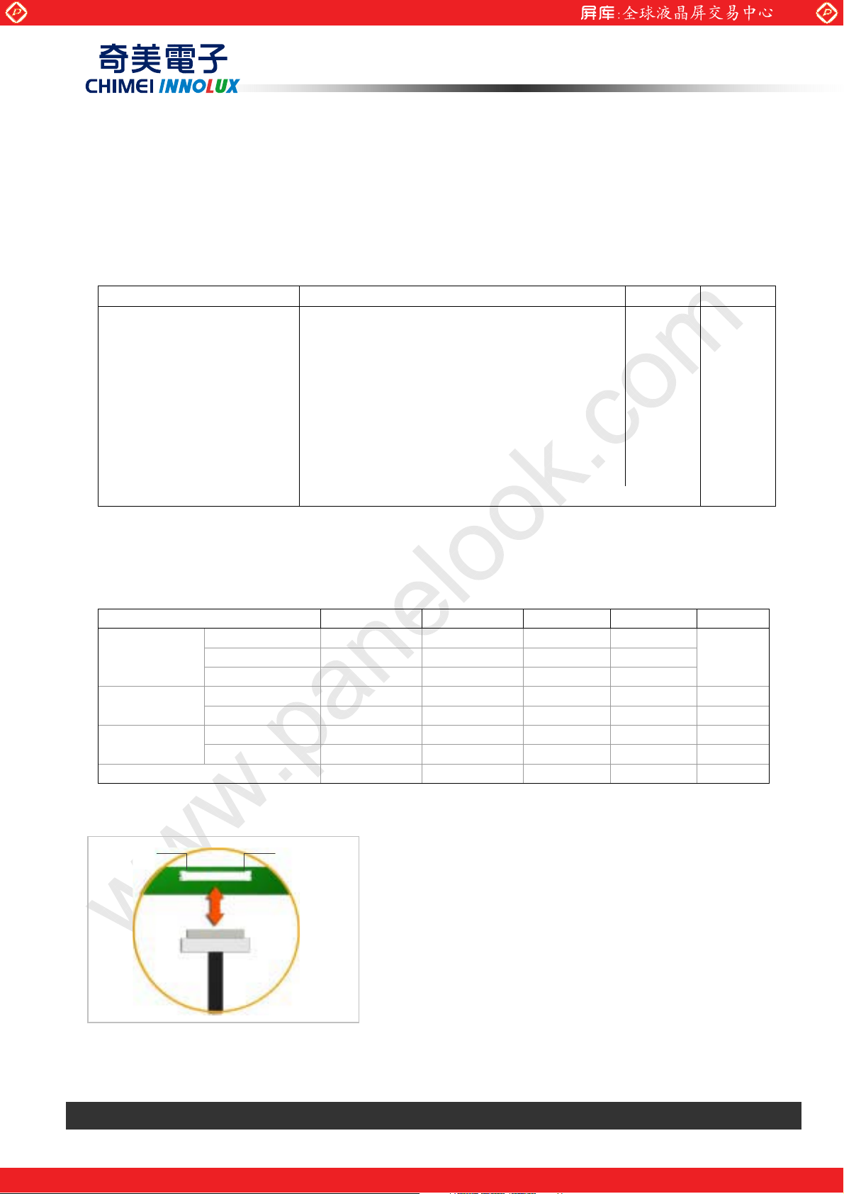
(1) Definition of dot defect
Define spec for 2 dot adjacent and minimum distance
2-adjacent(Linked Pixels)
Κsub-Pixel(R,G,B)
Minimum Distance;
Lit to LitΚLЇ=15mm
Unlit to UnlitΚLЇ=5mm
Lit to UnlitΚNot Applicable
L
L
L
L:Sub-Pixel to Sub-Pixel,Sub-Pixel to 2-adjacent or 2-adjacent to 2-adjacent
Version 3.0 27 January 2011 33 / 37
The copyright belongs to CHIMEI InnoLux. Any unauthorized use is prohibited.
One step solution for LCD / PDP / OLED panel application: Datasheet, inventory and accessory!
www.panelook.com
Page 34

Global LCD Panel Exchange Center
www.panelook.com
PRODUCT SPECIFICATION
(2) Display Inspection
a) Ambient Illumination: 250 Lux or more for light on inspection
b) Viewing Angle: Within LCD Viewing Angle Specification
c) Inspection Pattern (Bright dot): In black pattern
Inspection Pattern (Dark dot): In red, green , blue pattern
Items
XGA
WXGA
SXGA+
WXGA+
WSXGA+
UXGA
WUXGA
HD
HD+
FHD
N≦2 N≦2(G=1) N≦2(G=0) N≦2(G=0)
N≦1(G=0) N≦0 N≦0 N≦0
N≦0 N≦0 N≦0 N≦0
N≦3 N≦5 N≦10 N≦3
N≦1 N≦1 N≦2 N≦1
N≦0 N≦0 N≦0 N≦0
L≧15mm L≧15mm L≧15mm L≧15mm
L≧5mm L≧5mm L≧5mm L≧5mm
Bright dot
Dark dot
Distance
Random
2 dots adjacent
3 dots adjacent or
more
Random
2 dots adjacent
3 dots adjacent or
more
Lit to Lit
Unlit to Unlit
Lit to Unlit Not allowable Not allowable Not allowable Not allowable
Total bright and dark dot
N≦5
N≦7
(SXGA+
WXGA+)
N≦9
(WSXGA+)
N≦10
(UXGA)
N≦12
(WUXGA)
N≦5
˗˸˹˸˶˼˸ʳ˗ʳʻ˟˼˂˨˿˼ʼʳˍʳˡ˼˶˸˴˵˿˸ʳ˷˸˹˸˶˼˸ʳ˷ʳ˼ʳ˻˸ʳ˹˹˼˶˸ʳ˸˼˸ʳʻ˅ˈ˃ʳ˿ʼʳ˼˿˿ʳ˵˸ʳ˶˸˷ʳ
˸˺˴˷˿˸ʳ˹ʳ˷˸˹˸˶˼˸ʳ˷ʳ˼˸
Display failure (V-line/H-line/Cross line etc.) Not allowable
Mura
Mura defect can not show in 50% gray pattern with 8% ND-filter or judge by limit
sample if necessary
Version 3.0 27 January 2011 34 / 37
The copyright belongs to CHIMEI InnoLux. Any unauthorized use is prohibited.
One step solution for LCD / PDP / OLED panel application: Datasheet, inventory and accessory!
www.panelook.com
Page 35

Global LCD Panel Exchange Center
b
www.panelook.com
PRODUCT SPECIFICATION
(3) Appearance inspection
a) Ambient Illumination: 500 ~ 700 Lux
b) Viewing Angle: Backlight-Off Condition: At Right Angle To Polarizer Surface
Backlight-On Condition: Within LCD Viewing Angle Specification
c) Inspection Pattern: In White and 32-Gray(Half-Gray)Screens(Backlight-On)
Items Size(mm) Acceptable count
W<0.05 Ignore
1. Scratch(Line Shape)
: B/L –off condition
2. Dent
: B/L –off condition
3. Bubble
: B/L –off condition
4. Foreign material
(Line-shape: stain
inclusion)
:B/L-on condition
5. Foreign material
(Dot-shape: stain
inclusion)
:B/L-on condition
6. Peeling on Polizer edge
:B/L-off condition
a
D=(a+b)/2 W: width, LΚlength
0.05=<W<0.1; 0.3=<L=<3.0 N=<4
0.10=<W or 3.0<L N=0
Shall be no visible at B/L on.
D<0.2 Ignore
0.2=<D<0.5 N=<5
0.5=<D N=0
Spacing between defects shall be more than 30 mm.
(0.2=<D<0.5)
Shall be no visible at B/L on.
D<0.2 Ignore
0.2=<D<0.5 N=<5
0.5=<D N=0
Shall be no visible at B/L on.
W<0.05 Ignore
0.05=<W<0.10; 0.3<L=<2.0 N=<4
0.10<W or 2.0<L N=0
Shall be no visible at B/L on.
D<0.2 Ignore
0.2=<D<0.5 N=<5
0.5=<D N=0
D<0.2 Ignore
0.2=<D<0.5 N=<5
0.5=<D N=0
Bubble or glue shall not be visible within PC bezel
opening area with specified inspection viewing angle.
Continuous peeling off on polarizer edge shall be
discussed.
Shall be no visible at B/L on.
L
W
Version 3.0 27 January 2011 35 / 37
The copyright belongs to CHIMEI InnoLux. Any unauthorized use is prohibited.
One step solution for LCD / PDP / OLED panel application: Datasheet, inventory and accessory!
www.panelook.com
Page 36

Global LCD Panel Exchange Center
www.panelook.com
PRODUCT SPECIFICATION
E. External Appearance Inspection Criteria
Item Contents
Screw
CCFT cable
Metal frame
(Bezel)
Parts mounting, incomplete assembly, deformation, oxidized, crooked or rusty is not
permitted.
Cable not continuous、Break-off 、Connector Burn-off /Break-off
Scratch
*Noticeable scratch and exfoliation coating are not permitted.
*The oxidized metal is not permitted.
Incomplete assembly is not permitted.
Scratch The scratch which may causes a problem in practical use is not permitted.
Backlight
Break-off Breaking off is not permitted.
Crack The crack is not permitted.
Stain on
Polarizer
The stain which can’t be wiped off is not permitted.
Tape/Label Incorrect position, missed label is not permitted.
Connector Oxidized/rusty connector is not permitted.
Outline size Spec. out is not permitted.
Version 3.0 27 January 2011 36 / 37
The copyright belongs to CHIMEI InnoLux. Any unauthorized use is prohibited.
One step solution for LCD / PDP / OLED panel application: Datasheet, inventory and accessory!
www.panelook.com
Page 37

Global LCD Panel Exchange Center
www.panelook.com
PRODUCT SPECIFICATION
F. Classification of defects
Inspection Item Criteria and Description Defect type
Vertical line Signal input, vertical line off or irregular V-line appears major
Horizontal line Signal input, horizontal line off or irregular H-line appears major
Cross line Pattern signal input, a correct display is not obtained major
No display Signal input, display is dead major
Irregular display Pattern signal input, a correct display is not obtained major
Dots defect Exceed specified standards minor
Scratch and Dent
on polarizer
Exceed specified standards minor
Foreign material Exceed specified standards minor
Mura
External Appearance
Mura defect can not show in 50% gray pattern with 8% ND-filter
or judge by limit sample if necessary
Rust, deformation, irregular plating, coating missing etc.
A appearance defect that do not affect function or performance
minor
minor
Bezel claw Bezel claw missing or not bent major
Polarizer bubble Exceed specified standards minor
Flicker No noticeable flicker by naked eyes at any gray scale level major
In 50% gray pattern, hold LCD panel TOP edge (PCB side) by
LCD Pooling
both hands and swing slightly back and forth 2 times per second
minor
for 3 cycles by 15 degrees (Range 30 degrees)
Version 3.0 27 January 2011 37 / 37
The copyright belongs to CHIMEI InnoLux. Any unauthorized use is prohibited.
One step solution for LCD / PDP / OLED panel application: Datasheet, inventory and accessory!
www.panelook.com
 Loading...