

Page 1
PRODUCT SPECIFICATION
Customer:
Asus
Doc. Number:
□ Tentative Specification
□ Preliminary Specification
■ Approval Specification
MODEL NO.: N133HSG
SUFFIX: WJ1
APPROVED BY SIGNATURE
Name / Title
Note
Asus T31 Project
Please return 1 copy for your confirmation with your
signature and comments.
Approved By Checked By Prepared By
楊竣傑
2013-01-08
03:59:37 GMT
曹文彬
2013-01-07
08:44:57 GMT
陳郁甫
2013-01-04
05:37:42 GMT
Version 3.0 9 January 2013 1 / 44
The copyright belongs to CHIMEI InnoLux. Any unauthorized use is prohibited.
Page 2

PRODUCT SPECIFICATION
CONTENTS
1. GENERAL DESCRIPTION.........................................................................................................5
1.1 OVERVIEW..................................................................................................................5
1.2 GENERAL SPECIFICATI0NS......................................................................................5
2. MECHANICAL SPECIFICATIONS .............................................................................................6
2.1 CONNECTOR TYPE....................................................................................................6
3. ABSOLUTE MAXIMUM RATINGS .............................................................................................7
3.1 ABSOLUTE RATINGS OF ENVIRONMENT ...............................................................7
3.2 ELECTRICAL ABSOLUTE RATINGS.........................................................................7
3.2.1 TFT LCD MODULE............................................................................................................7
3.2.2 TOUCH PANEL ...................................................................................................................7
4. ELECTRICAL SPECIFICATIONS...............................................................................................8
4.1 FUNCTION BLOCK DIAGRAM...................................................................................8
4.2. INTERFACE CONNECTIONS ....................................................................................9
4.2.1 TOUCH PANEL MODULE.................................................................................................9
4.2.2 NON-TOUCH PANEL MODULE.......................................................................................9
4.2.3 TOUCH PANEL .................................................................................................................10
4.3 ELECTRICAL CHARACTERISTICS .........................................................................11
4.3.1 LCD ELETRONICS SPECIFICATION.............................................................................11
4.3.2 TOUCH PANEL ELETRONICS SPECIFICATION..........................................................13
4.3.3 LED CONVERTER SPECIFICATION..............................................................................14
4.3.4 BACKLIGHT UNIT...........................................................................................................16
4.4 DISPLAY PORT INPUT SIGNAL TIMING SPECIFICATIONS...................................17
4.4.1 ELECTRICAL SPECIFICATIONS....................................................................................17
4.5 DISPLAY TIMING SPECIFICATIONS........................................................................18
4.6 POWER ON/OFF SEQUENCE..................................................................................19
5. TOUCH GENERAL DESCRIPTION..........................................................................................22
5.1 GENERAL SPECIFICATI0NS....................................................................................22
5.2 Sensor Specification................................................................................................22
5.3 Optical Specification................................................................................................22
5.4 Touch Structure........................................................................................................22
6. OPTICAL CHARACTERISTICS ...............................................................................................23
6.1 TEST CONDITIONS ..................................................................................................23
6.2 OPTICAL SPECIFICATIONS.....................................................................................23
7. RELIABILITY TEST ITEM ........................................................................................................27
8. PACKING..................................................................................................................................28
8.1 MODULE LABEL.......................................................................................................28
Version 3.0 9 January 2013 2 / 44
The copyright belongs to CHIMEI InnoLux. Any unauthorized use is prohibited.
Page 3

PRODUCT SPECIFICATION
8.2 CARTON....................................................................................................................29
8.3 PALLET .....................................................................................................................30
9. PRECAUTIONS........................................................................................................................31
9.1 HANDLING PRECAUTIONS.....................................................................................31
9.2 STORAGE PRECAUTIONS ......................................................................................31
9.3 OPERATION PRECAUTIONS...................................................................................31
Appendix. EDID DATA STRUCTURE..........................................................................................32
Appendix. OUTLINE DRAWING..................................................................................................38
Appendix. SYSTEM COVER DESIGN NOTICE ..........................................................................40
Version 3.0 9 January 2013 3 / 44
The copyright belongs to CHIMEI InnoLux. Any unauthorized use is prohibited.
Page 4

REVISION HISTORY
PRODUCT SPECIFICATION
Version
3.0 Jan. 4, 2013 All Approval Spec Ver 3.0 was first issued for Asus.
Date Page Description
Version 3.0 9 January 2013 4 / 44
The copyright belongs to CHIMEI InnoLux. Any unauthorized use is prohibited.
Page 5
PRODUCT SPECIFICATION
1. GENERAL DESCRIPTION
1.1 OVERVIEW
N133HSG-WJ1 is a 13.3” Dual TFT Liquid Crystal Display module with LED Backlight unit and 30
pins eDP interface. This module supports 1920 x 1080 FHD mode and can display 16.7M colors.
The optimum viewing angle is at 6 o’clock direction.
1.2 GENERAL SPECIFICATI0NS
Item Specification Unit Note
Screen Size 13.3 diagonal
Driver Element a-si TFT active matrix - Pixel Number 1920 x R.G.B. x 1080 pixel Pixel Pitch 0.1529 (H) x 0.1529 (V) mm Pixel Arrangement RGB vertical stripe - Display Colors 16,777,216 color Transmissive Mode Normally black - Surface Treatment Hard coating (3H), Anti-Glare - Luminance, White 250/ Non-Touch Panel 280 Cd/m2
Backlight Unit LEDs 9 strings x 6 parallel
Type of Touch Module Windows Integrated Sensor (WIS)
Material of Touch Module Corning Fit
Touch Active Area (L x W) 296.96 x 168.44 mm
Touch Windows Visible Area
(L x W)
Simultaneous Sensing 10 Points
Touch Channels (X - Y) 70 - 40
Sensor Pitch (X - Y) 4.27 – 4.225 mm
Touch Panel Interface USB
Touch Panel Supply Voltage 3.3 V
Touch Panel Transmittance 85%
Touch Panel Reflectance <14% %
Touch Panel Haze <1% %
RoHs Compliance Yes
Power Consumption Total 5.924 W(Max.) @ cell 0.924W(Max.), BL 5.0 W(Max.) (1)
Note (1) The specified power consumption (with converter efficiency) is under the conditions at VCCS =
294.96 x 166.44 mm
3.3 V, fv = 60 Hz, LED_VCCS = Typ, fPWM = 200 Hz, Duty=100% and Ta = 25 ± 2 ºC, whereas mosaic
pattern is displayed.
Version 3.0 9 January 2013 5 / 44
The copyright belongs to CHIMEI InnoLux. Any unauthorized use is prohibited.
Page 6
PRODUCT SPECIFICATION
Pin1 Pin30
2. MECHANICAL SPECIFICATIONS
Item Min. Typ. Max. Unit Note
Horizontal (H) 337 337.2 337.4 mm
Module Size
(With Frame)
Non-Touch
Panel Side
Outline
Bezel Area
(Non-Touch
Panel Side)
Active Area
(Both Panel)
Note (1) Please refer to the attached drawings for more information of front and back outline dimensions.
Vertical (V) 224.61 224.81 225.01 mm
5.27
Thickness (T)
Horizontal (H)
With Bracket
Horizontal (H)
W/o Bracket
Vertical
With PCBA
Vertical
W/o PCBA
Horizontal 296.17 296.42 296.67 mm
Vertical 167.67 167.97 168.27 mm
Horizontal 293.46 293.76 294.06 mm
Vertical 164.94 165.24 165.54 mm
Weight -- -- 525 g
316.53 316.83 317.13 mm
305.05 305.35 305.65 mm
193 193.5 194 mm
183.11 183.41 183.71 mm
5.39* (w/
protect film)
5.53
5.65* (w/
protect film)
mm
(1)
Rear
cover:
AL 5052
Note* Do not consider the bubble because of the protect film.
2.1 CONNECTOR TYPE
Please refer Appendix Outline Drawing for detail design.
Connector Part No.:
User’s connector Part No:
IPEX-20455-030E-12
IPEX-20453-030T-01
Version 3.0 9 January 2013 6 / 44
The copyright belongs to CHIMEI InnoLux. Any unauthorized use is prohibited.
Page 7
PRODUCT SPECIFICATION
Storage Range
Operating Range
100
80 60 -20 40 0 20 -40
80
40
60
20
10
90
3. ABSOLUTE MAXIMUM RATINGS
3.1 ABSOLUTE RATINGS OF ENVIRONMENT
Item Symbol
Min. Max.
Storage Temperature TST -20 +60 ºC (1)
Operating Ambient Temperature TOP 0 +50 ºC (1), (2)
Note (1) (a) 90 %RH Max. (Ta <= 40 ºC).
(b) Wet-bulb temperature should be 39 ºC Max. (Ta > 40 ºC).
(c) No condensation.
Note (2) The temperature of panel surface should be 0 ºC min. and 60 ºC max.
Relative Humidity (%RH)
Value
Unit Note
Temperature (ºC)
3.2 ELECTRICAL ABSOLUTE RATINGS
3.2.1 TFT LCD MODULE
Item Symbol
Power Supply Voltage VCCS -0.3 +4.0 V
Logic Input Voltage VIN -0.3 +4.0 V
Converter Input Voltage
Converter Control Signal Voltage
Converter Control Signal Voltage
Note (1) Stresses beyond those listed in above “ELECTRICAL ABSOLUTE RATINGS” may cause
permanent damage to the device. Normal operation should be restricted to the conditions
described in “ELECTRICAL CHARACTERISTICS”.
LED_VCCS
LED_PWM,
LED_EN
Value
Min. Max.
-0.3 24 V (1)
-0.3 3.6 V 1)
-0.3 3.6 V (1)
Unit Note
(1)
3.2.2 TOUCH PANEL
Item Minimum Maximum
Analog Power Supply Voltage -0.5 4.6
Digital Power Supply Voltage -0.5 1.8
Version 3.0 9 January 2013 7 / 44
The copyright belongs to CHIMEI InnoLux. Any unauthorized use is prohibited.
Page 8
SCAN DRIVER IC
DC/DC CONVERTER &
SCAN D
RIVER IC
DC/DC C
ONVERTER &
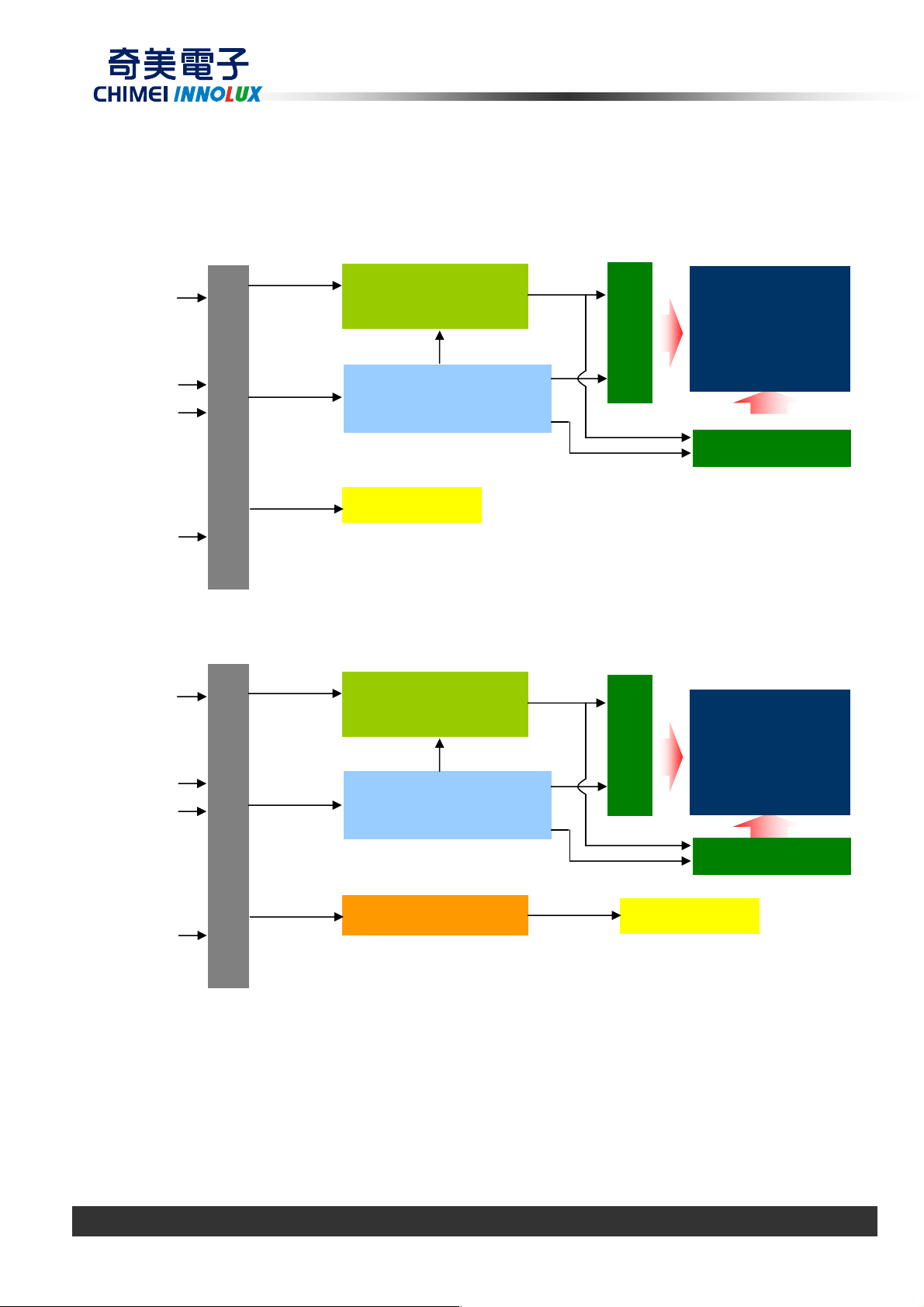
4. ELECTRICAL SPECIFICATIONS
4.1 FUNCTION BLOCK DIAGRAM
For A side Panel(TOUCH PANEL MODULE):
LVDS Display
Data & Clock
INPUT CONNECTOR
CONTROLLER
PRODUCT SPECIFICATION
TIMING
TFT LCD
PANEL
VCCS
REFERENCE VOLTAGE
GND
LED Light bar
Input Signals
LED Light bar
For B side Panel(NON-TOUCH PANEL MODULE):
LVDS Display
Data & Clock
VCCS
GND
INPUT CONNECTOR
CONTROLLER
REFERENCE VOLTAGE
GENERATOR
DATA DRIVER IC
TIMING
TFT LCD
PANEL
GENERATOR
Converter Input
Signals
Version 3.0 9 January 2013 8 / 44
DATA DRIVER IC
LED CONVERTER
The copyright belongs to CHIMEI InnoLux. Any unauthorized use is prohibited.
LED Light bar
Page 9
PRODUCT SPECIFICATION
4.2. INTERFACE CONNECTIONS
4.2.1 TOUCH PANEL MODULE
Pin Symbol Description Remark
1 NC No Connection (Reserved)
2 H_GND High Speed Ground
3 LANE1_N Complement Signal Link Lane 1
4 LANE1_P True Signal Link Lane 1
5 H_GND High Speed Ground
6 LANE0_N Complement Signal Link Lane 0
7 LANE0_P True Signal Link Lane 0
8 H_GND High Speed Ground
9 AUX_CH_P True Signal Auxiliary Channel
10 AUX_CH_N Complement Signal Auxiliary Channel
11 H_GND High Speed Ground
12 VCCS Power Supply +3.3 V (typical)
13 VCCS Power Supply +3.3 V (typical)
14 BIST
15 GND Ground
16 GND Ground
17 HPD Hot Plug Detect
18 NC No Connection (Reserved)
19 NC No Connection (Reserved)
20 LB_FB1 LED Light bar feedback CH1 (Cathode). 22mA
21 LB_FB2 LED Light bar feedback CH2 (Cathode). 22mA
22 LB_FB3 LED Light bar feedback CH3 (Cathode). 22mA
23 LB_FB4 LED Light bar feedback CH4 (Cathode). 22mA
24 LB_FB5 LED Light bar feedback CH5 (Cathode). 22mA
25 LB_FB6 LED Light bar feedback CH6 (Cathode). 22mA
26 NC No Connection (Reserved)
27 NC No Connection (Reserved)
28 LB_VCC LED Light bar VCC. 25.2~29.7V
29 LB_VCC LED Light bar VCC. 25.2~29.7V
30 LOGO_VCCS LOGO LED Power Supply +5V, (typical)
LCD Panel Self Test Enable(Reserved for CMI
test)
4.2.2 NON-TOUCH PANEL MODULE
Pin Symbol Description Remark
1
2
3
4
5
6
7
8
9
10
NC No Connection (Reserved)
H_GND High Speed Ground
LANE1_N Complement Signal Link Lane 1
LANE1_P True Signal Link Lane 1
H_GND High Speed Ground
LANE0_N Complement Signal Link Lane 0
LANE0_P True Signal Link Lane 0
H_GND High Speed Ground
AUX_CH_P True Signal Auxiliary Channel
AUX_CH_N Complement Signal Auxiliary Channel
Version 3.0 9 January 2013 9 / 44
The copyright belongs to CHIMEI InnoLux. Any unauthorized use is prohibited.
Page 10
PRODUCT SPECIFICATION
Pitch
11
12
13
14
15
16
17
18
19
20
21
22
23
24
25
26
27
28
29
30
H_GND High Speed Ground
VCCS Power Supply +3.3 V (typical)
VCCS Power Supply +3.3 V (typical)
BIST LCD Panel Self Test Enable
GND Ground
GND Ground
HPD Hot Plug Detect
BL_GND Backlight Ground
BL_GND Backlight Ground
BL_GND Backlight Ground
BL_GND Backlight Ground
LED_EN Backlight Enable Signal of LED Converter
LED_PWM
PWM Dimming Control Signal of LED
Converter
NC No Connection (Reserved)
NC No Connection (Reserved)
LED_VCCS Backlight Power
LED_VCCS Backlight Power
LED_VCCS Backlight Power
LED_VCCS Backlight Power
NC No Connection (Reserved)
4.2.3 TOUCH PANEL
Pin. Description Remark
1 CGND
2 GND
3 USBN
4 USBP
5 3.3V
6 DNU
7 DNU
8 DNU
9 DNU
10 CGND
Note (1) The first pixel is odd as shown in the following figure.
1,2
(even)
2,2
1,3
(odd)
1,4
(even)
1,1
(odd)
2,1
3,1
Pitch
1,Xmax
Ymax,1
Ymax,
Xmax
Version 3.0 9 January 2013 10 / 44
The copyright belongs to CHIMEI InnoLux. Any unauthorized use is prohibited.
Page 11
4.3 ELECTRICAL CHARACTERISTICS
C2
4.3.1 LCD ELETRONICS SPECIFICATION
For A side Panel(TOUCH PANEL MODULE):
PRODUCT SPECIFICATION
Parameter Symbol
Unit Note
Min. Typ. Max.
Power Supply Voltage VCCS 3.0 3.3 3.6 V (1)-
High Level 2.25 - 2.75 V
HPD
Low Level 0 - 0.4 V
Ripple Voltage VRP - 50 - mV (1)-
Value
Inrush Current I
- - 1.5 A (1),(2)
RUSH
Mosaic 220 250 280 mA (3)a
Power Supply Current
White
lcc
250 280 310 mA (3)b
For B side Panel(NON-TOUCH PANEL MODULE):
Value
Parameter Symbol
Unit Note
Min. Typ. Max.
Power Supply Voltage VCCS 3.0 3.3 3.6 V (1)-
High Level 2.25 - 2.75 V
HPD
Low Level 0 - 0.4 V
Ripple Voltage VRP - 50 - mV (1)Inrush Current I
- - 1.5 A (1),(2)
RUSH
Mosaic 240 270 300 mA (3)a
Power Supply Current
White
lcc
270 300 330 mA (3)b
Note (1) The ambient temperature is Ta = 25 ± 2 ºC.
Note (2) I
: the maximum current when VCCS is rising
RUSH
IIS: the maximum current of the first 100ms after power-on
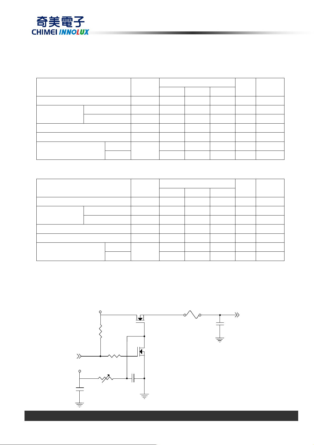
Measurement Conditions: Shown as the following figure. Test pattern: black.
+3.3V
Q1 2SK1475
(High to Low)
(Control Signal)
SW
+12V
C1
1uF
VR1
R1
47K
47K
R2
1K
0.01uF
Q2
2SK1470
FUSE
C3
1uF
VCCS
(LCD Module Input)
Version 3.0 9 January 2013 11 / 44
The copyright belongs to CHIMEI InnoLux. Any unauthorized use is prohibited.
Page 12
PRODUCT SPECIFICATION
VCCS rising time is 0.5ms
Version 3.0 9 January 2013 12 / 44
The copyright belongs to CHIMEI InnoLux. Any unauthorized use is prohibited.
Page 13
PRODUCT SPECIFICATION
Note (3) The specified power supply current is under the conditions at VCCS = 3.3 V, Ta = 25 ± 2 ºC, DC
Current and fv = 60 Hz, whereas a power dissipation check pattern below is displayed.
a. Mosaic Pattern
Active Area
b. White Pattern
Active Area
4.3.2 TOUCH PANEL ELETRONICS SPECIFICATION
Item Symbol
3.3V Power Supply Voltage VDDE 3.0 3.3 3.6 V
1.2V Power Supply Voltage VDD 1.14 1.2 1.26 V
Specification
Min. Typ. Max.
Unit Remark
Version 3.0 9 January 2013 13 / 44
The copyright belongs to CHIMEI InnoLux. Any unauthorized use is prohibited.
Page 14
PRODUCT SPECIFICATION
PWM Control Permissive Ripple
4.3.3 LED CONVERTER SPECIFICATION
For B side Panel(NON-TOUCH PANEL MODULE)
Parameter Symbol
Value
Unit Note
Min. Typ. Max.
Converter Input power supply voltage
LED_Vccs
Converter Inrush Current
Backlight On 3 - 3.6 V
EN Control Level
Backlight Off
PWM High Level
PWM Control Level
PWM Low Level
PWM Control Duty Ratio
Voltage
V
PWM Control Frequency f
LED Power Current LED_VCCS =Typ.
Note (1):LED light bar configuration is shown as below.
IL
+
LB_VCC
Light Bar Feedback Channels
I
CH1
I
CHn
-
7 12.0 21.0 V
ILED
RUSH
- - 1.5 A (2)
0 - 0.5 V
3 - 3.6 V
0 - 0.5 V
10 - 100 %
5 - 100 % (3)
PWM_pp
190 - 2K Hz (4)
PWM
- - 100 mV
ILED 299 357 413 mA (5)
PS:IL =(I
CH1
+..+I
CHn
)mA
LED Light Bar
Note(2)LED
: the maximum current when LED_VCCS is rising,
RUSH
ILEDIS: the maximum current of the first 100ms after power-on,
Measurement Conditions: Shown as the following figure. LED_VCCS = Typ, Ta = 25 ± 2 ºC, f
= 200 Hz, Duty=100%.
Version 3.0 9 January 2013 14 / 44
The copyright belongs to CHIMEI InnoLux. Any unauthorized use is prohibited.
PWM
Page 15

PRODUCT SPECIFICATION
≤∗+
∗+≤
C2
LED_VCCS(Typ)
Q1 IRL3303
R1
47K
FUSE
C3
1uF
(LED Converter Input)
(High to Low)
(Control Signal)
SW=24V
LED_VCCS(Typ)
R2
1K
47K
VR1
C1
1uF
0.01uF
Q2
IRL3303
VLED rising time is 0.5ms
0.5ms
90%
LED_VCC
0V
10%
LED_PWM
0V
100ms
LED_EN
0V
ILED
Rush
ILED
IS
ILED
Note (3) If the PWM control duty ratio is less than 10%, there is some possibility that acoustic noise or
backlight flash can be found. And it is also difficult to control the brightness linearity.
Note (4) If PWM control frequency is applied in the range less than 1KHz, the “waterfall” phenomenon on
the screen may be found. To avoid the issue, it’s a suggestion that PWM control frequency should
follow the criterion as below.
PWM control frequency f
fN )33.0(
should be in the range
PWM
f
PWM
fN
)66.0(
Version 3.0 9 January 2013 15 / 44
The copyright belongs to CHIMEI InnoLux. Any unauthorized use is prohibited.
Page 16

PRODUCT SPECIFICATION
≥
N
: Integer
f
: Frame rate
Note (5) The specified LED power supply current is under the conditions at “LED_VCCS = Typ.”, Ta = 25
)3(
N
± 2 ºC, f
= 200 Hz, Duty=100%.
PWM
4.3.4 BACKLIGHT UNIT
Parameter Symbol
LED Light Bar Power
Supply Voltage
LED Light Bar Power
Supply Current
Power Consumption PL - 3.564 3.9204 W (3)
LED Life Time LBL 12,000 - - Hrs (4)
Note (1) LED current is measured by utilizing a high frequency current meter as shown below :
Light Bar Feedback
Channels
VL 25.2 27 29.7 V
IL 132 mA
Min. Typ. Max.
V
L, IL
Ta = 25 ± 2 ºC
Value
LED
Light Bar
Unit Note
(1)(2)(Duty100%)
Note (2) For better LED light bar driving quality, it is recommended to utilize the adaptive boost converter
with current balancing function to drive LED light-bar.
Note (3) PL = IL ×VL (With LED converter transfer efficiency)
Note (4) The lifetime of LED is defined as the time when it continues to operate under the conditions at Ta =
25 ±2 oC and IL = 20 mA(per EA) until the brightness becomes 50% of its original value.≦
Version 3.0 9 January 2013 16 / 44
The copyright belongs to CHIMEI InnoLux. Any unauthorized use is prohibited.
Page 17

PRODUCT SPECIFICATION
0V
VCM
|VID|
4.4 DISPLAY PORT INPUT SIGNAL TIMING SPECIFICATIONS
4.4.1 ELECTRICAL SPECIFICATIONS
Parameter Symbol Min. Typ. Max. Unit Notes
Differential Signal Common Mode
Voltage(MainLink and AUX)
AUX AC Coupling Capacitor C
Note (1) Display port interface related AC coupled signals should follow VESA DisplayPort Standard
Version1. Revision 1a and VESA Embedded DisplayPortTM Standard Version 1.1.
(2) The AUX AC Coupling Capacitor should be placed on Source Devices.
(3)The source device should pass the test criteria described in DisplayPortCompliance Test
Specification (CTS) 1.1
VCM 0 2 V (1)(3)
75 200 nF (2)
AUX
VD+
Single Ended
VD-
Version 3.0 9 January 2013 17 / 44
The copyright belongs to CHIMEI InnoLux. Any unauthorized use is prohibited.
Page 18

PRODUCT SPECIFICATION
4.5 DISPLAY TIMING SPECIFICATIONS
The input signal timing specifications are shown as the following table and timing diagram.
Refresh rate 60Hz
Signal Item Symbol Min. Typ. Max. Unit Note
DCLK Frequency 1/Tc 136.86 138.78 140.69 MHz
Vertical Total Time 1102 1112
Vertical Active Display Period 1080 1080 1080 1080
DE
Note (1) Because this module is operated by DE only mode, Hsync and Vsync are ignored.
Vertical Active Blanking Period TV-TVD
Horizontal Total Time 2070 2080 2090 2070
Horizontal Active Display Period 1920 1920 1920 1920
Horizontal Active Blanking Period
INPUT SIGNAL TIMING DIAGRAM
TH-THD
32 TV-TVD TV-TVD TH -
160
1122 1102 TH -
TH-THD TH-THD
-
TH -
Tc Tc Tc -
DE
DCLK
DE
DATA
TC
THD
Version 3.0 9 January 2013 18 / 44
The copyright belongs to CHIMEI InnoLux. Any unauthorized use is prohibited.
Page 19

4.6 POWER ON/OFF SEQUENCE
10%
t6
PRODUCT SPECIFICATION
TOUCH PANEL MODULE:
-Power Supply
for LCD, VCCS
-eDP Display
-HPD from Sink
-AUX Channel
-Main Link Data
0V
Power On
90%
10%
0V
Power Off
t11
90%
t1
t2
Black Video
t3
AUX Channel Operational
t4
Link
Training
t7
Idle
Video from Source
Valid Video Data
t10
Black Video
Idle or off
Restart
10%
t12
- LB Power
LB_VCC
0V
t5
t8
90%
10%
t9
90%
10%
t
A
t
B
Version 3.0 9 January 2013 19 / 44
The copyright belongs to CHIMEI InnoLux. Any unauthorized use is prohibited.
Page 20

PRODUCT SPECIFICATION
10%
t6
-
-
-
-Power Supply
for LCD, VCCS
-eDP Display
-HPD from Sink
-AUX Channel
NON-TOUCH PANEL MODULE:
-Main Link Data
0V
0V
Power On
90%
10%
t1
Power Off
t11
90%
t2
Black Video
t3
AUX Channel Operational
t4
Link
Training
t7
Idle
Video from Source
Valid Video Data
t10
Black Video
Idle or off
Restart
10%
t12
Power Supply for
LED Converter,
LED_VCCS
LED Converter
Dimming Signal,
LED_PWM
LED Converter
Enable Signal,
LED_EN
0V
0V
0V
10%
t5
90%
t8
t
A
t
C
t
E
t9
90%
10%
t
B
t
D
t
F
Version 3.0 9 January 2013 20 / 44
The copyright belongs to CHIMEI InnoLux. Any unauthorized use is prohibited.
Page 21

PRODUCT SPECIFICATION
Timing Specifications: Follow VESA Embedded Display Port Standard Version 1
Parameter
t1 Power rail rise time, 10% to 90%
t2
t3
t4
t5 Link training duration Source
t6 Link idle Source
t7
t8
t9
t10
t11
t12 VCCS Power off time Source
tA
tB
tC
tD
tE
tF
Note (1) Please don’t plug or unplug the interface cable when system is turned on.
Delay from LCD,VCCS to black
video generation
Delay from LCD,VCCS to HPD
high
Delay from HPD high to link
training initialization
Delay from valid video data from
Source to video on display
Delay from valid video data from
Source to backlight on
Delay from backlight off to end of
valid video data
Delay from end of valid video data
from Source to power off
VCCS power rail fall time, 90% to
10%
LED power rail rise time, 10% to
90%
LED power rail fall time, 90% to
10%
Delay from LED power rising to
LED dimming signal
Delay from LED dimming signal to
LED power falling
Delay from LED dimming signal to
LED enable signal
Delay from LED enable signal to
LED dimming signal
Description
Reqd.
By
Source 0.5 10 ms -
Sink 0 200 ms Sink 0 200 ms -
Source - - ms
Sink 0 50 ms
Source
Source - - ms
Source 0 500 ms
Source 0.5 10 ms
Source 0.5 10 ms
Source 0 10 ms
Source 10 - ms
Source 10 - ms
Source 10 - ms Source 10 - ms -
Value
Min Max
- - ms
- - ms
- - ms
500 - ms
Unit Notes
-
-
-
-
-
-
-
-
-
-
-
-
-
Note (2) Please avoid floating state of the interface signal during signal invalid period.
Note (3) It is recommended that the backlight power must be turned on after the power supply for LCD and the
interface signal is valid
Version 3.0 9 January 2013 21 / 44
The copyright belongs to CHIMEI InnoLux. Any unauthorized use is prohibited.
Page 22

PRODUCT SPECIFICATION
5. TOUCH GENERAL DESCRIPTION
5.1 GENERAL SPECIFICATI0NS
Item Specification Unit Note
Supply Voltage
Oscillator Frequency
Interface
Support OS
Support Points
Min. Report Rate
Resolution
Power Consumption
Touch Panel RAW count
5.2 Sensor Specification
Glass Corning_FIT 0.55 mm
BM 1.4um
ITO Sheet Resistance <50 ohm/sq
OC1 1.6um
Matel Sheet Resistance <0.3 ohm/sq
OC2 2.3um
3.3
32M
USB
WIN8
10
100
1920*1080
(1) Action:~380mW, (2) Idle:300mW, (3) Off:0W
N/A
Item Spec
V
Hz
-
-
-
Hz
-
-
-
5.3 Optical Specification
Transmittance (min.) >85%
Haze (Max.) <1%
Chromaticity (a*,b*) (Max.) NA
Reflection (Max.) <14%
Transmittance Chromaticity NA
Reflectivicity Chromaticity NA
5.4 Touch Structure
Sensor structure Module structure
Version 3.0 9 January 2013 22 / 44
The copyright belongs to CHIMEI InnoLux. Any unauthorized use is prohibited.
Page 23

PRODUCT SPECIFICATION
6. OPTICAL CHARACTERISTICS
6.1 TEST CONDITIONS
Item Symbol Value Unit
Ambient Temperature Ta
Ambient Humidity Ha
25±2
50±10
Supply Voltage VCC 3.3 V
Input Signal According to typical value in "3. ELECTRICAL CHARACTERISTICS"
LED Light Bar Input Current IL 132 mA
The measurement methods of optical characteristics are shown in Section 5.2. The following items
should be measured under the test conditions described in Section 5.1 and stable environment shown in
Note (5).
6.2 OPTICAL SPECIFICATIONS
Item Symbol Condition Min. Typ. Max. Unit
Contrast Ratio CR 500 700 - - (2),(5),(9)
Response Time
Cross Talk
Average Luminance of White
(Touch Panel Module)
Average Luminance of White
(Non-Touch Panel Module)
Red
Color
Green
Chromaticity
(Touch Panel Module)
Blue
White
Red
Color
Green
Chromaticity
(Non-Touch Panel Module)
Blue
White
Color Gamut CG - 72 - % (5),(8),(9)
Horizontal
Viewing Angle
Vertical
White Variation of 5 Points δW5p θx=0°, θY =0°
TR - 14 19 ms
TF - 11 16 ms
CT
L
L
Rx
Ry
Gx
Gy
Bx
By
AVE
AVE
θ
Viewing Normal
=0°, θY =0°
x
Angle
- - 4 % (7)
210 250
235
280
- cd/m
- cd/m
0.650
0.338
0.329
0.608
0.148
0.047
Wx 0.318
Wy 0.334
Rx
Ry
Gx
Gy
Bx
By
Typ –
0.03
0.650
0.338
0.329
0.608
0.148
0.047
Typ +
0.03
Wx 0.313
Wy
θ
+
x
θ
x
θ
Y
θ
Y
+
85 89
CR≥10
-
85 89 85 89 85 89 -
0.329
70 80 - % (5),(6),(9)
o
C
%RH
Note
(3),(9)
2
(4),(6),(9)
2
(4),(6),(9)
-
-
-
-
-
-
-
(1),(5),(9)
-
-
-
-
-
-
-
-
Deg. (1),(5),(9)
Version 3.0 9 January 2013 23 / 44
The copyright belongs to CHIMEI InnoLux. Any unauthorized use is prohibited.
Page 24

Note (1) Definition of Viewing Angle (θx, θy):
T
ime
66.67 ms
66.67 ms
PRODUCT SPECIFICATION
Normal
θx = θy = 0º
θ
X-
= 90º
x-
6 o’clock
θ
y-
= 90º
y-
Note (2) Definition of Contrast Ratio (CR):
The contrast ratio can be calculated by the following expression.
Contrast Ratio (CR) = L63 / L0
L63: Luminance of gray level 63
L 0: Luminance of gray level 0
CR = CR (1)
θy- θ
θx−
y+
θx+
12 o’clock direction
y+
θ
y+
= 90º
x+
θ
X+
= 90º
CR (X) is corresponding to the Contrast Ratio of the point X at Figure in Note (6).
Note (3) Definition of Response Time (TR, TF):
100%
90%
Optical
Response
10%
0%
TR
Note (4) Definition of Average Luminance of White (L
Measure the luminance of gray level 63 at 5 points
L
= [L (1)+ L (2)+ L (3)+ L (4)+ L (5)] / 5
AVE
L (x) is corresponding to the luminance of the point X at Figure in Note (6)
AVE
TF
):
Version 3.0 9 January 2013 24 / 44
The copyright belongs to CHIMEI InnoLux. Any unauthorized use is prohibited.
Page 25

Note (5) Measurement Setup:
Light Shield Room
( Ambient
L
uminance < 2
l u x)
X=1 to 13
X
The LCD module should be stabilized at given temperature for 20 minutes to avoid abrupt
temperature change during measuring. In order to stabilize the luminance, the measurement
should be executed after lighting Backlight for 20 minutes in a windless room.
LCD M odule
PRODUCT SPECIFICATION
LCD P anel
USB2000
or equivalent
CS - 2000T
or equivalent
Center of the S creen
500 mm
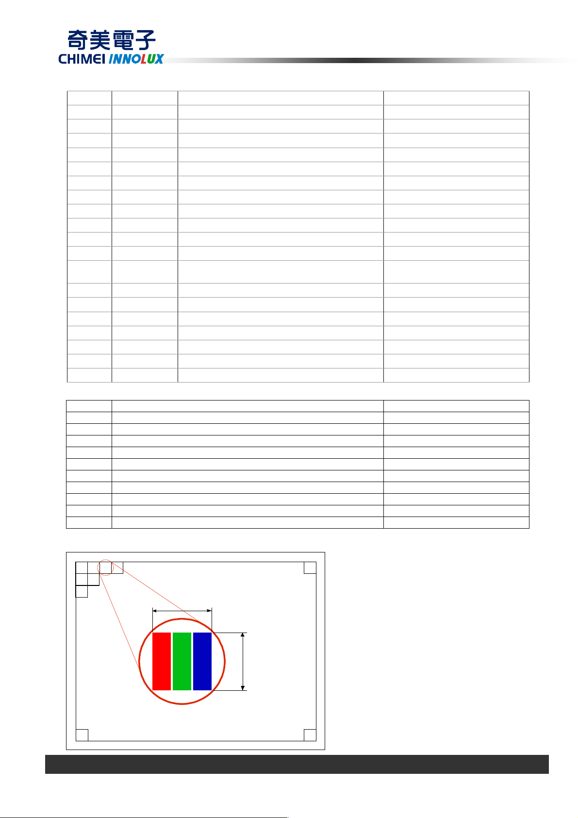
Note (6) Definition of White Variation (δW):
Measure the luminance of gray level 63 at 5 points
δW5p = {
Minimum [L (1) ~ L (5)] / Maximum [L (1) ~ L (5)]}*100%
10mm
6
H/4
2 3
7
8
: Test Point
Version 3.0 9 January 2013 25 / 44
H
H/4 H/4 H/4
The copyright belongs to CHIMEI InnoLux. Any unauthorized use is prohibited.
9
4 5
11 12 13
10mm 10mm
10mm
W/4 W/4 W/4 W/4
1
W
10
Active area
Page 26

PRODUCT SPECIFICATION
Note (7) Cross Talk (CT):
CT= ∣YB - YA∣/ YA ×100%
Where
YA=Luminance of measured location in left figure
YB=Luminance of measured location in right figure
Note (8) Definition of color gamut (C.G%):
C.G%= Area (R, G, B) / Area (R0, G0, B0,)* 100%
R0, G0, B0: CIE1931 coordinates of red, green, and blue defined by NTSC.
R, G, B: CIE1931 coordinates of red, green, and blue in module at 63 gray level.
Area (R0, G0, B0): Area of the triangle defined by coordinate R0, G0, B0.
Area(R, G, B): Area of the triangle defined by coordinate R, G, B
CIE 1931
0.9
0.8
0.7
0.6
0.5
0.4
0.3
0.2
0.1
0
0 0.2 0.4 0. 6 0. 8
G
0
G
R
0
R
B
B
0
Note (9) The listed optical specifications refer to the initial value of manufacture, but the condition of
the specifications after long-term operation will not be warranted.
Version 3.0 9 January 2013 26 / 44
The copyright belongs to CHIMEI InnoLux. Any unauthorized use is prohibited.
Page 27

PRODUCT SPECIFICATION
7. RELIABILITY TEST ITEM
Test Item Test Condition Note
High Temperature Storage Test 60ºC, 240 hours
Low Temperature Storage Test -20ºC, 240 hours
Thermal Shock Storage Test
-20ºC, 0.5hour←→60℃, 0.5hour; 100cycles, 1hour/cycle
High Temperature Operation Test 50ºC, 240 hours
Low Temperature Operation Test 0ºC, 240 hours
High Temperature & High Humidity
Operation Test
ESD Test (Operation)
Shock (Non-Operating)
Vibration (Non-Operating)
Note (1) criteria : Normal display image with no obvious non-uniformity and no line defect.
Note (2) Evaluation should be tested after storage at room temperature for more than two hour
Note (3) At testing Vibration and Shock, the fixture in holding the module has to be hard and rigid enough
so that the module would not be twisted or bent by the fixture.
50ºC, RH 80%, 240hours
150pF, 330Ω, 1sec/cycle
Condition 1 : Contact Discharge, ±8KV
Condition 2 : Air Discharge, ±15KV
220G, 2ms, half sine wave,1 time for each direction of
±X,±Y,±Z
1.5G / 10-500 Hz, Sine wave, 30 min/cycle, 1cycle for each
X, Y, Z
(1) (2)
(1)
(1)(3)
(1)(3)
Version 3.0 9 January 2013 27 / 44
The copyright belongs to CHIMEI InnoLux. Any unauthorized use is prohibited.
Page 28

PRODUCT SPECIFICATION
8. PACKING
8.1 MODULE LABEL
The barcode nameplate is pasted on each module as illustration, and its definitions are as following explanation.
N133HSG-WJ1
X X X X X X X Y M D L N N N N
(a) Model Name: N133HSG – WJ1
(b) Revision: Rev. XX, for example: C1, C2 …etc.
(c) Serial ID: X X X X X X X Y M D L N N N N
Serial ID includes the information as below:
(a) Manufactured Date: Year: 0~9, for 2010~2019
Month: 1~9, A~C, for Jan. ~ Dec.
Day: 1~9, A~Y, for 1st to 31st, exclude I , O and U
(b) Revision Code: cover all the change
(c) Serial No.: Manufacturing sequence of product
(d) Product Line: 1 -> Line1, 2 -> Line 2, …etc.
Serial No.
Product Line
Year, Month, Date
CMO Internal Use
Revision
CMO Internal Use
Version 3.0 9 January 2013 28 / 44
The copyright belongs to CHIMEI InnoLux. Any unauthorized use is prohibited.
Page 29

8.2 CARTON
PRODUCT SPECIFICATION
Figure. 7-2 Packing method
Version 3.0 9 January 2013 29 / 44
The copyright belongs to CHIMEI InnoLux. Any unauthorized use is prohibited.
Page 30

8.3 PALLET
PRODUCT SPECIFICATION
Figure. 7-3 Packing method
Version 3.0 9 January 2013 30 / 44
The copyright belongs to CHIMEI InnoLux. Any unauthorized use is prohibited.
Page 31

PRODUCT SPECIFICATION
9. PRECAUTIONS
9.1 HANDLING PRECAUTIONS
(1) The module should be assembled into the system firmly by using every mounting hole. Be careful
not to twist or bend the module.
(2) While assembling or installing modules, it can only be in the clean area. The dust and oil may cause
electrical short or damage the polarizer.
(3) Use fingerstalls or soft gloves in order to keep display clean during the incoming inspection and
assembly process.
(4) Do not press or scratch the surface harder than a HB pencil lead on the panel because the polarizer
is very soft and easily scratched.
(5) If the surface of the polarizer is dirty, please clean it by some absorbent cotton or soft cloth. Do not
use Ketone type materials (ex. Acetone), Ethyl alcohol, Toluene, Ethyl acid or Methyl chloride. It
might permanently damage the polarizer due to chemical reaction.
(6) Wipe off water droplets or oil immediately. Staining and discoloration may occur if they left on panel
for a long time.
(7) If the liquid crystal material leaks from the panel, it should be kept away from the eyes or mouth. In
case of contacting with hands, legs or clothes, it must be washed away thoroughly with soap.
(8) Protect the module from static electricity, it may cause damage to the C-MOS Gate Array IC.
(9) Do not disassemble the module.
(10) Do not pull or fold the LED wire.
(11) Pins of I/F connector should not be touched directly with bare hands.
(12) Always using two hands to hold and handle the modules. And do not hold the corner.
9.2 STORAGE PRECAUTIONS
(1) High temperature or humidity may reduce the performance of module. Please store LCD module
within the specified storage conditions.
(2) It is dangerous that moisture come into or contacted the LCD module, because the moisture may
damage LCD module when it is operating.
(3) It may reduce the display quality if the ambient temperature is lower than 10 ºC. For example, the
response time will become slowly, and the starting voltage of LED will be higher than the room
temperature.
9.3 OPERATION PRECAUTIONS
(1) Do not pull the I/F connector in or out while the module is operating.
(2) Always follow the correct power on/off sequence when LCD module is connecting and operating.
This can prevent the CMOS LSI chips from damage during latch-up.
(3) The startup voltage of Backlight is approximately 1000 Volts. It may cause electrical shock while
assembling with converter. Do not disassemble the module or insert anything into the Backlight unit.
Version 3.0 9 January 2013 31 / 44
The copyright belongs to CHIMEI InnoLux. Any unauthorized use is prohibited.
Page 32

PRODUCT SPECIFICATION
Appendix. EDID DATA STRUCTURE
The EDID (Extended Display Identification Data) data formats are to support displays as defined in the
VESA Plug & Display and FPDI standards.
Touch Panel Module:
Byte #
(decimal)
10
11
12
13
14
15
16
17
18
19
20
21
22
23
24
25
26
27
28
29
30
31
32
33
34
35
36
37
38
39
40
0
1
2
3
4
5
6
7
8
9
Byte #
(hex)
0 Header
1 Header
2 Header
3 Header
4 Header
5 Header
6 Header
7 Header
8 EISA ID manufacturer name (“CMN”)
9 EISA ID manufacturer name (Compressed ASCII)
0A ID product code (N133HSG-WJ1) 46
0B ID product code (hex LSB first; N133HSG-WJ1) 13
0C ID S/N (fixed “0”)
0D ID S/N (fixed “0”)
0E ID S/N (fixed “0”)
0F ID S/N (fixed “0”)
10 Week of manufacture (fixed week code)
11 Year of manufacture (fixed year code)
12 EDID structure version # (“1”)
13 EDID revision # (“4”)
14 Vedio Input Definition
15 Max H image size (“28.186cm”)
16 Max V image size (“16.524cm”)
17 Display Gamma (Gamma = ”2.2”)
18 Feature support
19 Red/Green (Rx1, Rx0, Ry1, Ry0, Gx1, Gx0, Gy1, Gy0)
1A Blue/White (Bx1, Bx0, By1, By0, Wx1, Wx0, Wy1, Wy0)
1B Red-x (Rx = “0.662”)
1C Red-y (Ry = “0.325”)
1D Green-x (Gx = ”0.296”)
1E Green-y (Gy = ”0.588”)
1F Blue-x (Bx = ”0.146")
20 Blue-y (By = ”0.068”)
21 White-x (Wx = ”0.311”)
22 White-y (Wy = ”0.325”)
23 Established timings 1
24 Established timings 2
25 Manufacturer’s reserved timings
26 Standard timing ID # 1
27 Standard timing ID # 1
28 Standard timing ID # 2
Field Name and Comments
Value
(hex)
00 00000000
FF 11111111
FF 11111111
FF 11111111
FF 11111111
FF 11111111
FF 11111111
00 00000000
0D 00001101
AE 10101110
00 00000000
00 00000000
00 00000000
00 00000000
34 00110100
15 00010101
01 00000001
04 00000100
A5 10100101
1C 00011100
10 00010000
78 01111000
02 00000010
93 10010011
AD 10101101
A9 10101001
53 01010011
4C 01001100
96 10010110
25 00100101
11 00010001
4F 01001111
53 01010011
00 00000000
00 00000000
00 00000000
01 00000001
01 00000001
01 00000001
Value
(binary)
01000110
00010011
Version 3.0 9 January 2013 32 / 44
The copyright belongs to CHIMEI InnoLux. Any unauthorized use is prohibited.
Page 33

PRODUCT SPECIFICATION
41
42
43
44
45
46
47
48
49
50
51
52
53
54
55
56
57
58
59
60
61
62
63
64
65
66
67
68
69
70
71
72
73
74
75
76
77
78
79
80
81
82
83
84
29 Standard timing ID # 2
2A Standard timing ID # 3
2B Standard timing ID # 3
2C Standard timing ID # 4
2D Standard timing ID # 4
2E Standard timing ID # 5
2F Standard timing ID # 5
30 Standard timing ID # 6
31 Standard timing ID # 6
32 Standard timing ID # 7
33 Standard timing ID # 7
34 Standard timing ID # 8
35 Standard timing ID # 8
Detailed timing description # 1 Pixel clock (“138.78MHz”, According to
36
VESA CVT Rev1.4)
37 # 1 Pixel clock (hex LSB first)
38 # 1 H active (“1920”)
39 # 1 H blank (“160”)
3A # 1 H active : H blank (“1920 :160”)
3B # 1 V active (”1080”)
3C # 1 V blank (”32”)
3D # 1 V active : V blank (”1080 :32”)
3E # 1 H sync offset (”46”)
3F # 1 H sync pulse width ("30”)
40 # 1 V sync offset : V sync pulse width (”2 : 4”)
# 1 H sync offset : H sync pulse width : V sync offset : V sync width
41
(”46: 30 : 2 : 4”)
42 # 1 H image size (”282 mm”)
43 # 1 V image size (”165 mm”)
44 # 1 H image size : V image size (”282 : 165”)
45 # 1 H boarder (”0”)
46 # 1 V boarder (”0”)
# 1 Non-interlaced, Normal, no stereo, Separate sync, H/V pol
47
Negatives
Detailed timing description # 2 Pixel clock (“92.52MHz”, According to
VESA CVT Rev1.4)
48
49 # 2 Pixel clock (hex LSB first)
4A # 2 H active (“1920”)
4B # 2 H blank (“160”)
4C # 2 H active : H blank (“1920 :160”)
4D # 2 V active (”1080”)
4E # 2 V blank (”32”)
4F # 2 V active : V blank (”1080 :32”)
50 # 2 H sync offset (”46”)
51 # 2 H sync pulse width ("30”)
52 # 2 V sync offset : V sync pulse width (”2 : 4”)
# 2 H sync offset : H sync pulse width : V sync offset : V sync width
53
(”46: 30 : 2 : 4”)
54 # 1 H image size (”282 mm”)
01 00000001
01 00000001
01 00000001
01 00000001
01 00000001
01 00000001
01 00000001
01 00000001
01 00000001
01 00000001
01 00000001
01 00000001
01 00000001
36 00110110
36 00110110
80 10000000
A0 10100000
70 01110000
38 00111000
20 00100000
40 01000000
2E 00101110
1E 00011110
24 00100100
00 00000000
1A 00011010
A5 10100101
10 00010000
00 00000000
00 00000000
18 00011000
24 00100100
24 00100100
80 10000000
A0 10100000
70 01110000
38 00111000
20 00100000
40 01000000
2E 00101110
1E 00011110
24 00100100
00 00000000
1A 00011010
Version 3.0 9 January 2013 33 / 44
The copyright belongs to CHIMEI InnoLux. Any unauthorized use is prohibited.
Page 34

PRODUCT SPECIFICATION
85
86
87 57 # 2 H boarder (”0”) 00 00000000
88
89
90
91
92
93
94
95
96
97
98
99
100
101
102
103
104
105
106
107
108
109
110
111
112
113
114
115
116
117
118
119
120
121
122
123
124
125
126
127
55 # 1 V image size (”165 mm”)
56 # 1 H image size : V image size (”282 : 165”)
58 # 2 V boarder (”0”)
# 2 Non-interlaced, Normal, no stereo, Separate sync, H/V pol
Negatives
59
5A Detailed timing description # 3
5B # 3 Flag
5C # 3 Reserved
5D # 3 FE (hex) defines ASCII string (Vendor “CMN”, ASCII)
5E # 3 Flag
5F # 3 1st character of string (“C”)
60 # 3 2nd character of string (“M”)
61 # 3 3rd character of string (“N”)
62 # 3 New line character indicates end of ASCII string
63 # 3 Padding with “Blank” character
64 # 3 Padding with “Blank” character
65 # 3 Padding with “Blank” character
66 # 3 Padding with “Blank” character
67 # 3 Padding with “Blank” character
68 # 3 Padding with “Blank” character
69 # 3 Padding with “Blank” character
6A # 3 Padding with “Blank” character
6B # 3 Padding with “Blank” character
6C Detailed timing description # 4
6D # 4 Flag
6E # 4 Reserved
# 4 FE (hex) defines ASCII string (Model Name“N133HSG-WJ1”,
ASCII)
6F
70 # 4 Flag
71 # 4 1st character of name (“N”) 4E
72 # 4 2nd character of name (“1”) 31
73 # 4 3rd character of name (“3”) 33
74 # 4 4th character of name (“3”) 33
75 # 4 5th character of name (“H”) 48
76 # 4 6th character of name (“S”) 53
77 # 4 7th character of name (“G”) 47
78 # 4 8th character of name (“-”) 2D
79 # 4 9th character of name (“W”)
7A # 4 Ath character of name (“J”)
7B # 4 Bth character of name (“1”)
7C # 4 New line character indicates end of ASCII string
7D # 4 Padding with “Blank” character
7E No extension
7F Checksum
A5 10100101
10 00010000
00 00000000
18 00011000
00 00000000
00 00000000
00 00000000
FE 11111110
00 00000000
43 01000011
4D 01001101
4E 01001110
0A 00001010
20 00100000
20 00100000
20 00100000
20 00100000
20 00100000
20 00100000
20 00100000
20 00100000
20 00100000
00 00000000
00 00000000
00 00000000
FE 11111110
00 00000000
57 01010111
4A 01001010
31 00110001
0A 00001010
20 00100000
00 00000000
AD 10101101
01001110
00110001
00110011
00110011
01001000
01010011
01000111
00101101
Version 3.0 9 January 2013 34 / 44
The copyright belongs to CHIMEI InnoLux. Any unauthorized use is prohibited.
Page 35

Non-Touch Panel Module
Byte #
(decimal)
10
11
12
13
14
15
16
17
18
19
20
21
22
23
24
25
26
27
28
29
30
31
32
33
34
35
36
37
38
39
40
41
42
43
0
1
2
3
4
5
6
7
8
9
Byte #
(hex)
0 Header
1 Header
2 Header
3 Header
4 Header
5 Header
6 Header
7 Header
8 EISA ID manufacturer name (“CMN”)
9 EISA ID manufacturer name (Compressed ASCII)
0A ID product code (N133HSG-WJ1) 47
0B ID product code (hex LSB first; N133HSG-WJ1) 13
0C ID S/N (fixed “0”)
0D ID S/N (fixed “0”)
0E ID S/N (fixed “0”)
0F ID S/N (fixed “0”)
10 Week of manufacture (fixed week code)
11 Year of manufacture (fixed year code)
12 EDID structure version # (“1”)
13 EDID revision # (“4”)
14 Vedio Input Definition
15 Max H image size (“28.186cm”)
16 Max V image size (“16.524cm”)
17 Display Gamma (Gamma = ”2.2”)
18 Feature support
19 Red/Green (Rx1, Rx0, Ry1, Ry0, Gx1, Gx0, Gy1, Gy0)
1A Blue/White (Bx1, Bx0, By1, By0, Wx1, Wx0, Wy1, Wy0)
1B Red-x (Rx = “0.662”)
1C Red-y (Ry = “0.325”)
1D Green-x (Gx = ”0.296”)
1E Green-y (Gy = ”0.588”)
1F Blue-x (Bx = ”0.146")
20 Blue-y (By = ”0.068”)
21 White-x (Wx = ”0.311”)
22 White-y (Wy = ”0.325”)
23 Established timings 1
24 Established timings 2
25 Manufacturer’s reserved timings
26 Standard timing ID # 1
27 Standard timing ID # 1
28 Standard timing ID # 2
29 Standard timing ID # 2
2A Standard timing ID # 3
2B Standard timing ID # 3
PRODUCT SPECIFICATION
Field Name and Comments
Value
(hex)
00 00000000
FF 11111111
FF 11111111
FF 11111111
FF 11111111
FF 11111111
FF 11111111
00 00000000
0D 00001101
AE 10101110
00 00000000
00 00000000
00 00000000
00 00000000
34 00110100
15 00010101
01 00000001
04 00000100
A5 10100101
1C 00011100
10 00010000
78 01111000
02 00000010
93 10010011
AD 10101101
A9 10101001
53 01010011
4C 01001100
96 10010110
25 00100101
11 00010001
4F 01001111
53 01010011
00 00000000
00 00000000
00 00000000
01 00000001
01 00000001
01 00000001
01 00000001
01 00000001
01 00000001
Value
(binary)
01000111
00010011
Version 3.0 9 January 2013 35 / 44
The copyright belongs to CHIMEI InnoLux. Any unauthorized use is prohibited.
Page 36

PRODUCT SPECIFICATION
44
45
46
47
48
49
50
51
52
53
54
55
56
57
58
59
60
61
62
63
64
65
66
67
68
69
70
71
72
73
74
75
76
77
78
79
80
81
82
83
84
85
86
87 57 # 2 H boarder (”0”) 00 00000000
2C Standard timing ID # 4
2D Standard timing ID # 4
2E Standard timing ID # 5
2F Standard timing ID # 5
30 Standard timing ID # 6
31 Standard timing ID # 6
32 Standard timing ID # 7
33 Standard timing ID # 7
34 Standard timing ID # 8
35 Standard timing ID # 8
Detailed timing description # 1 Pixel clock (“138.78MHz”, According to
36
VESA CVT Rev1.4)
37 # 1 Pixel clock (hex LSB first)
38 # 1 H active (“1920”)
39 # 1 H blank (“160”)
3A # 1 H active : H blank (“1920 :160”)
3B # 1 V active (”1080”)
3C # 1 V blank (”32”)
3D # 1 V active : V blank (”1080 :32”)
3E # 1 H sync offset (”46”)
3F # 1 H sync pulse width ("30”)
40 # 1 V sync offset : V sync pulse width (”2 : 4”)
# 1 H sync offset : H sync pulse width : V sync offset : V sync width
41
(”46: 30 : 2 : 4”)
42 # 1 H image size (”282 mm”)
43 # 1 V image size (”165 mm”)
44 # 1 H image size : V image size (”282 : 165”)
45 # 1 H boarder (”0”)
46 # 1 V boarder (”0”)
# 1 Non-interlaced, Normal, no stereo, Separate sync, H/V pol
47
Negatives
Detailed timing description # 2 Pixel clock (“92.52MHz”, According to
VESA CVT Rev1.4)
48
49 # 2 Pixel clock (hex LSB first)
4A # 2 H active (“1920”)
4B # 2 H blank (“160”)
4C # 2 H active : H blank (“1920 :160”)
4D # 2 V active (”1080”)
4E # 2 V blank (”32”)
4F # 2 V active : V blank (”1080 :32”)
50 # 2 H sync offset (”46”)
51 # 2 H sync pulse width ("30”)
52 # 2 V sync offset : V sync pulse width (”2 : 4”)
# 2 H sync offset : H sync pulse width : V sync offset : V sync width
53
(”46: 30 : 2 : 4”)
54 # 1 H image size (”282 mm”)
55 # 1 V image size (”165 mm”)
56 # 1 H image size : V image size (”282 : 165”)
01 00000001
01 00000001
01 00000001
01 00000001
01 00000001
01 00000001
01 00000001
01 00000001
01 00000001
01 00000001
36 00110110
36 00110110
80 10000000
A0 10100000
70 01110000
38 00111000
20 00100000
40 01000000
2E 00101110
1E 00011110
24 00100100
00 00000000
1A 00011010
A5 10100101
10 00010000
00 00000000
00 00000000
18 00011000
24 00100100
24 00100100
80 10000000
A0 10100000
70 01110000
38 00111000
20 00100000
40 01000000
2E 00101110
1E 00011110
24 00100100
00 00000000
1A 00011010
A5 10100101
10 00010000
Version 3.0 9 January 2013 36 / 44
The copyright belongs to CHIMEI InnoLux. Any unauthorized use is prohibited.
Page 37

PRODUCT SPECIFICATION
88
89
90
91
92
93
94
95
96
97
98
99
100
101
102
103
104
105
106
107
108
109
110
111
112
113
114
115
116
117
118
119
120
121
122
123
124
125
126
127
58 # 2 V boarder (”0”)
# 2 Non-interlaced, Normal, no stereo, Separate sync, H/V pol
59
Negatives
5A Detailed timing description # 3
5B # 3 Flag
5C # 3 Reserved
5D # 3 FE (hex) defines ASCII string (Vendor “CMN”, ASCII)
5E # 3 Flag
5F # 3 1st character of string (“C”)
60 # 3 2nd character of string (“M”)
61 # 3 3rd character of string (“N”)
62 # 3 New line character indicates end of ASCII string
63 # 3 Padding with “Blank” character
64 # 3 Padding with “Blank” character
65 # 3 Padding with “Blank” character
66 # 3 Padding with “Blank” character
67 # 3 Padding with “Blank” character
68 # 3 Padding with “Blank” character
69 # 3 Padding with “Blank” character
6A # 3 Padding with “Blank” character
6B # 3 Padding with “Blank” character
6C Detailed timing description # 4
6D # 4 Flag
6E # 4 Reserved
# 4 FE (hex) defines ASCII string (Model Name“N133HSG-WJ1”,
6F
ASCII)
70 # 4 Flag
71 # 4 1st character of name (“N”) 4E
72 # 4 2nd character of name (“1”) 31
73 # 4 3rd character of name (“3”) 33
74 # 4 4th character of name (“3”) 33
75 # 4 5th character of name (“H”) 48
76 # 4 6th character of name (“S”) 53
77 # 4 7th character of name (“G”) 47
78 # 4 8th character of name (“-”) 2D
79 # 4 9th character of name (“W”)
7A # 4 Ath character of name (“J”)
7B # 4 Bth character of name (“1”)
7C # 4 New line character indicates end of ASCII string
7D # 4 Padding with “Blank” character
7E No extension
7F Checksum
00 00000000
18 00011000
00 00000000
00 00000000
00 00000000
FE 11111110
00 00000000
43 01000011
4D 01001101
4E 01001110
0A 00001010
20 00100000
20 00100000
20 00100000
20 00100000
20 00100000
20 00100000
20 00100000
20 00100000
20 00100000
00 00000000
00 00000000
00 00000000
FE 11111110
00 00000000
01001110
00110001
00110011
00110011
01001000
01010011
01000111
00101101
57 01010111
4A 01001010
31 00110001
0A 00001010
20 00100000
00 00000000
AC 10101100
Version 3.0 9 January 2013 37 / 44
The copyright belongs to CHIMEI InnoLux. Any unauthorized use is prohibited.
Page 38

Appendix. OUTLINE DRAWING
PRODUCT SPECIFICATION
Version 3.0 9 January 2013 38 / 44
The copyright belongs to CHIMEI InnoLux. Any unauthorized use is prohibited.
Page 39

PRODUCT SPECIFICATION
Version 3.0 9 January 2013 39 / 44
The copyright belongs to CHIMEI InnoLux. Any unauthorized use is prohibited.
Page 40

PRODUCT SPECIFICATION
Appendix. SYSTEM COVER DESIGN NOTICE
1. Design gap A between panel & any components on system cover
a). At least 0.5mm gap between panel & system is recommended for preventing from
backpack or pogo test fail.
Definition
2 Design gap B1 & B2 between panel & protrusions
b). Zero gap from panel's maximum thickness boundary to any components, foreign objects,
wire, cable or extrusion on system cover inner surface is forbidden.
B1
Protrusion
Protrusion
B2
2.0mm min. gap is recommended between panel & protrusions for preventing from shock
Definition
related failures.
Version 3.0 9 January 2013 40 / 44
The copyright belongs to CHIMEI InnoLux. Any unauthorized use is prohibited.
Page 41

PRODUCT SPECIFICATION
3 Design gap C between system front bezel & panel surface.
a). Sufficient gap between system front bezel & panel surface is a must for preventing from
pooling or glass broken.
b). Zero gap or interference is forbidden.
Definition
4 Design gap D1 & D2 between system front bezel & PCB Assembly.
c). Zero gap is also forbidden in the act of system front bezel deformation during swing test,
hinge test, knock test, or during pooling inspection procedure.
d). To remain sufficient gap, design with system rib higher than maximum panel thickness is
recommended.
a). Sufficient gap between system front bezel & PCB assembly is a must for preventing from
abnormal display after backpack test, hinge test, twist test or pogo test.
b). Zero gap or interference is forbidden.
Definition
c). Zero gap is also forbidden in the act of system front bezel deformation during hinge test,
twist test, or during pooling inspection procedure.
d). To remain sufficient gap, design with system rib higher than maximum panel thickness is
recommended.
Version 3.0 9 January 2013 41 / 44
The copyright belongs to CHIMEI InnoLux. Any unauthorized use is prohibited.
Page 42

PRODUCT SPECIFICATION
5 Interference examination of antenna cable and WebCam wire
a). Antenna cable or WebCam wire overlap with panel outline is forbidden for preventing
from abnormal display & white spot after backpack test, hinge test, twist test or pogo test.
Definition
6 System inner surface examination
b). Antenna cable or WebCam wire bypass panel outline is recommended.
Definition a). Burr at logo edge, step, protrusion or PCB board will easily cause white spot or glass
broken.
b). Keeping flat surface underneath backlight is recommended.
7 Tape/sponge design on system inner surface
Version 3.0 9 January 2013 42 / 44
The copyright belongs to CHIMEI InnoLux. Any unauthorized use is prohibited.
Page 43

PRODUCT SPECIFICATION
Definition a) To prevent abnormal display & white spot after scuffing test, hinge test, pogo test,
backpack test, it is not recommended to add tape/sponge in separate location. Since each
tape/sponge may act as pressure concentration location.
b) We suggest to design with a tape/sponge that well covered under panel rear cover.
8 Assembly SOP examination
Definition To prevent panel crack during system front bezel assembly process with hook design, it is
prohibited to press panel or any location that related directly to the panel.
9 Material used for system rear bezel
Definition To prevent panel crack during system front bezel assembly process without hook design, it
is only allowed to give slight pressure with large contact area. This can help to distribute the
stress and prevent stress concentration. Also it is suggest to put the system on a flat surface
stage during the assembly.
10 Material used for system rear bezel
Version 3.0 9 January 2013 43 / 44
The copyright belongs to CHIMEI InnoLux. Any unauthorized use is prohibited.
Page 44

PRODUCT SPECIFICATION
Definition a) To prevent abnormal display & white spot after scuffing test, hinge test, pogo test,
backpack test, as the poor rigidity result from deformation of system rear cover during the
test.
b) We suggest using aluminum-magnesium alloy as the rear frame material with thickness
min 1.5mm, instead of using PC/ABS.
11 System base unit design near keyboard and mouse pad
Definition To prevent abnormal display & white spot after scuffing test, hinge test, pogo test, backpack
test, no sharp edge design is allowed in any area that may damage the panel during the
test. We suggest to remove all sharp edges, or to reduce the thickness difference of
keyboard/mouse pad from the nearby surface.
12 Screw boss height design
Definition a). Gap left between panel rear cover bracket and screw boss surface is prohibited.
b). To remain sufficient gap between panel and system rear bezel, screw boss height must
be designed with respet to the height of bracket bottom surface to panel bottom surface +
flatness change of panel itself.
Version 3.0 9 January 2013 44 / 44
The copyright belongs to CHIMEI InnoLux. Any unauthorized use is prohibited.
 Loading...