

Page 1
Global LCD Panel Exchange Center
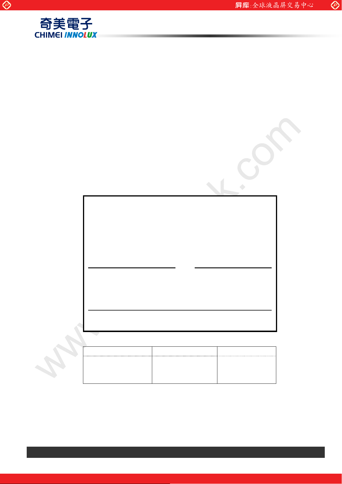
Customer:
MODEL NO.: N133HSG
www.panelook.com
PRODUCT SPECIFICATION
Doc. Number:
Ϯ Tentative Specification
ϭ Preliminary Specification
ϭ Approval Specification
SUFFIX: DJ1
APPROVED BY SIGNATURE
Name / Title
Note
Please return 1 copy for your confirmation with your
signature and comments.
Approved By Checked By Prepared By
Version 0.0 10 July 2012 1 / 26
copyright belongs to CHIMEI InnoLux. Any unauthorized use is prohibited.
One step solution for LCD / PDP / OLED panel application: Datasheet, inventory and accessory!
www.panelook.com
Page 2
Global LCD Panel Exchange Center
www.panelook.com
PRODUCT SPECIFICATION
CONTENTS
1. GENERAL DESCRIPTION .........................................................................................................4
1.1 OVERVIEW ........................................................................................................................... 4
1.2 GENERAL SPECIFICATI0NS................................................................................................4
2. MECHANICAL SPECIFICATIONS .............................................................................................5
2.1 CONNECTOR TYPE.............................................................................................................. 5
3. ABSOLUTE MAXIMUM RATINGS .............................................................................................6
3.1 ABSOLUTE RATINGS OF ENVIRONMENT ....................................................................... 6
3.2 ABSOLUTE RATINGS OF ENVIRONMENT (OPEN CELL) ............................................... 6
3.3 ELECTRICAL ABSOLUTE RATINGS(OPEN CELL)........................................................... 7
3.3.1 TFT LCD MODULE ........................................................................................................7
4. ELECTRICAL SPECIFICATIONS............................................................................................... 8
4.1 FUNCTION BLOCK DIAGRAM........................................................................................... 8
4.2. INTERFACE CONNECTIONS.............................................................................................. 8
4.3 ELECTRICAL CHARACTERISTICS .................................................................................. 10
4.3.1 LCD ELETRONICS SPECIFICATION..........................................................................10
4.3.2 LED CONVERTER SPECIFICATION...........................................................................12
4.4 DISPLAY PORT SIGNAL TIMING SPECIFICATION......................................................... 14
4.4.1 DISPLAY PORT INTERFACE........................................................................................... 14
4.5 DISPLAY TIMING SPECIFICATIONS................................................................................ 15
4.6 POWER ON/OFF SEQUENCE ............................................................................................ 16
5. OPTICAL CHARACTERISTICS ............................................................................................... 18
5.1 TEST CONDITIONS ............................................................................................................ 18
5.2 OPTICAL SPECIFICATIONS .............................................................................................. 18
6. PACKING.................................................................................................................................. 21
6.1 CMI OPEN CELL LABEL ................................................................................................... 21
6.2 PACKAGE RELIABILITY................................................................................................... 22
6.3 CARTON .............................................................................................................................. 22
6.4 PALLET................................................................................................................................ 23
7. PRECAUTIONS ........................................................................................................................24
7.1 HANDLING PRECAUTIONS.............................................................................................. 24
7.2 STORAGE PRECAUTIONS ................................................................................................ 24
7.3 OPERATION PRECAUTIONS............................................................................................. 24
Appendix. EDID DATA STRUCTURE.......................................................................................... 25
Appendix. OUTLINE DRAWING.................................................................................................. 25
Version 0.0 10 July 2012 2 / 26
copyright belongs to CHIMEI InnoLux. Any unauthorized use is prohibited.
One step solution for LCD / PDP / OLED panel application: Datasheet, inventory and accessory!
www.panelook.com
Page 3
Global LCD Panel Exchange Center
www.panelook.com
PRODUCT SPECIFICATION
REVISION HISTORY
Version
0.0 Jul.10, 2012 All Spec. Ver. 0.0 was first issued.
Date Page Description
Version 0.0 10 July 2012 3 / 26
copyright belongs to CHIMEI InnoLux. Any unauthorized use is prohibited.
One step solution for LCD / PDP / OLED panel application: Datasheet, inventory and accessory!
www.panelook.com
Page 4
Global LCD Panel Exchange Center
1. GENERAL DESCRIPTION
1.1 OVERVIEW
N133HSG-DJ1 is a 13.3” TFT Liquid Crystal Display with 30 pins eDP interface. This product
supports 1920 x 1080 FHD mode and can display 16,7M colors. The backlight unit is not built in.
1.2 GENERAL SPECIFICATI0NS
Item Specification Unit Note
Screen Size 13.3 diagonal
Driver Element a-si TFT active matrix - Pixel Number 1920 x R.G.B. x 1080 pixel Pixel Pitch 0.1529 (H) x 0.1529 (V) mm Pixel Arrangement RGB vertical stripe - Display Colors 16,777,216 (8 bit) color Transmissive Mode Normally Black - Surface Treatment Hard coating (3H), Anti-Glare - -
www.panelook.com
PRODUCT SPECIFICATION
Version 0.0 10 July 2012 4 / 26
copyright belongs to CHIMEI InnoLux. Any unauthorized use is prohibited.
One step solution for LCD / PDP / OLED panel application: Datasheet, inventory and accessory!
www.panelook.com
Page 5
Global LCD Panel Exchange Center
Pin1 Pin30
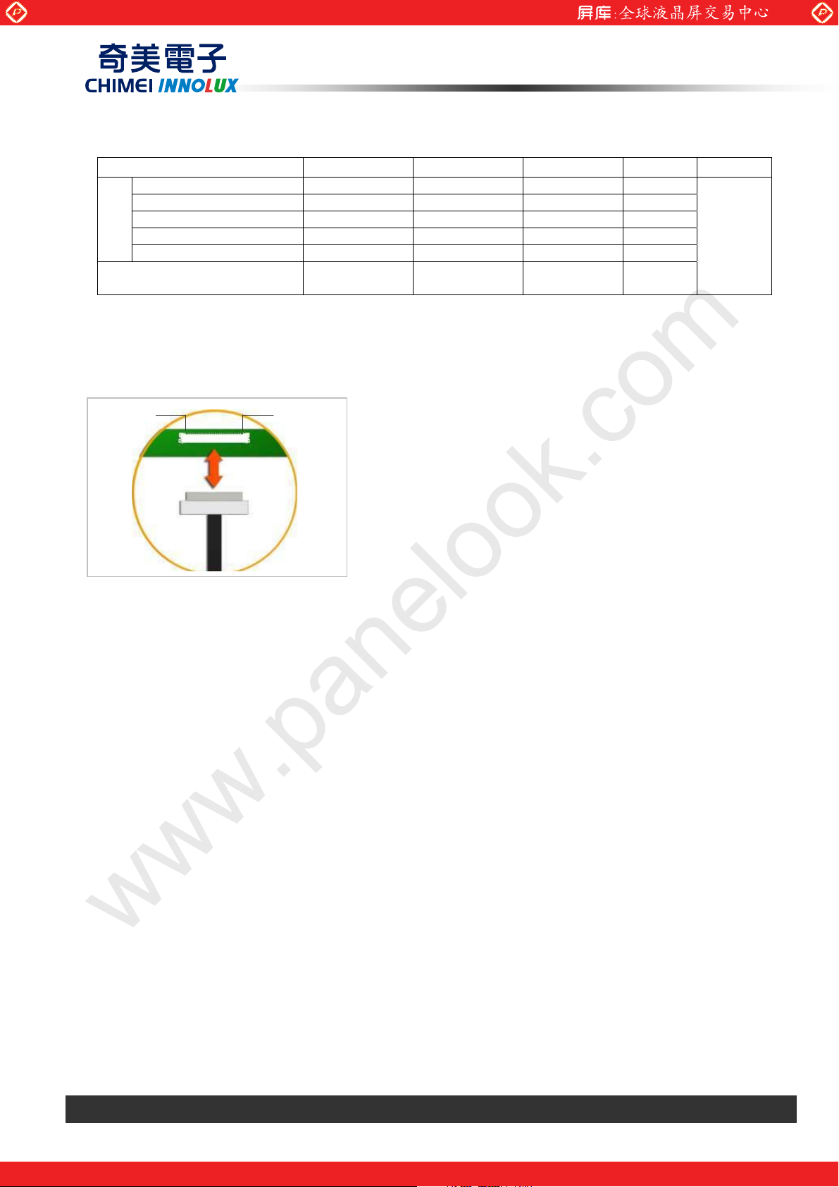
2. MECHANICAL SPECIFICATIONS
item Min. Typ. Max. Unit Note
Horizontal (H) with PCB 301.77 301.97 302.17 mm
Vertical (V) with PCB 186.44 187.44 188.44 mm
Size
Vertical (V) w/o PCB 174.99 175.19 175.39 mm
Thickness (T) with PCB - - 2.0 mm
Thickness (T) w/o PCB - 0.87 0.95- mm
Weight
(with polarizer release paper)
Note (1) Please refer to the attached drawings for more information of front and back outline dimensions.
(2) Connector mounting position
2.1 CONNECTOR TYPE
www.panelook.com
PRODUCT SPECIFICATION
(1) (2)
- 115 125 g
Please refer Appendix Outline Drawing for detail design.
Connector Part No.: IPEX-20455-030E-12 or equivalent
User’s connector Part No: IPEX-20453-030T-01 or equivalent
2.1.2 LED Light-Bar Connector
Connector Part No.: STM MSK24022P10A or equivalent
Version 0.0 10 July 2012 5 / 26
copyright belongs to CHIMEI InnoLux. Any unauthorized use is prohibited.
One step solution for LCD / PDP / OLED panel application: Datasheet, inventory and accessory!
www.panelook.com
Page 6
Global LCD Panel Exchange Center
3. ABSOLUTE MAXIMUM RATINGS
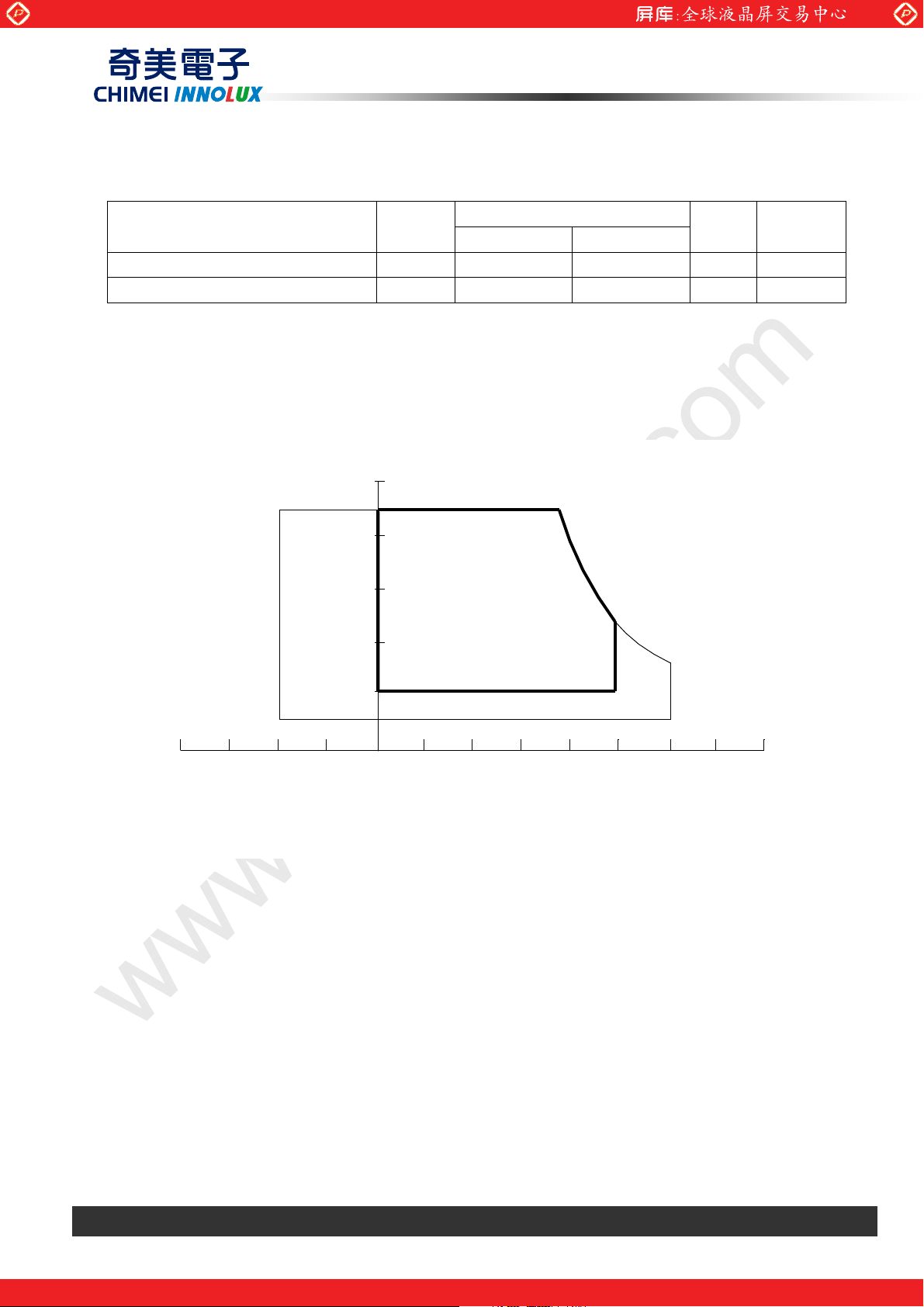
3.1 ABSOLUTE RATINGS OF ENVIRONMENT
Item Symbol
Storage Temperature TST -20 +60 ºC (1)
Operating Ambient Temperature TOP 0 +50 ºC (1), (2)
Note (1) (a) 90 %RH Max. (Ta <= 40 ºC).
(b) Wet-bulb temperature should be 39 ºC Max. (Ta > 40 ºC).
(c) No condensation.
Note (2) The temperature of panel surface should be 0 ºC min. and 60 ºC max.
Relative Humidity (%RH)
www.panelook.com
PRODUCT SPECIFICATION
Val ue
Min. Max.
Unit Note
100
90
80
60
Operating
40
20
10
Storage Range
80 60 -20 40 0 20 -40
Temperature (ºC)
3.2 ABSOLUTE RATINGS OF ENVIRONMENT (OPEN CELL)
High temperature or humidity may reduce the performance of panel. Please store LCD panel within the
specified storage conditions.
Storage Condition: With packing.
Storage temperature range: 25±5 ºC.
Storage humidity range: 50±10%RH.
Shelf life: 30days
Version 0.0 10 July 2012 6 / 26
copyright belongs to CHIMEI InnoLux. Any unauthorized use is prohibited.
One step solution for LCD / PDP / OLED panel application: Datasheet, inventory and accessory!
www.panelook.com
Page 7
Global LCD Panel Exchange Center
System PWM signal input for
3.3 ELECTRICAL ABSOLUTE RATINGS(OPEN CELL)
3.3.1 TFT LCD MODULE
Item Symbol
Power Supply Voltage VCCS -0.3 +4.0 V
Logic Input Voltage VIN -0.3 VCCS+0.3
dimming
Color Engine CE_EN -0.3 5 V
Dynamic backlight control CABC_EN -0.3 5 V
Note (1) Stresses beyond those listed in above “ELECTRICAL ABSOLUTE RATINGS” may cause
permanent damage to the device. Normal operation should be restricted to the conditions
described in “ELECTRICAL CHARACTERISTICS”.
www.panelook.com
PRODUCT SPECIFICATION
Min. Max.
PWM_IN
-0.3 5 V
Val ue
Unit Note
(1)
V
Version 0.0 10 July 2012 7 / 26
copyright belongs to CHIMEI InnoLux. Any unauthorized use is prohibited.
One step solution for LCD / PDP / OLED panel application: Datasheet, inventory and accessory!
www.panelook.com
Page 8
Global LCD Panel Exchange Center
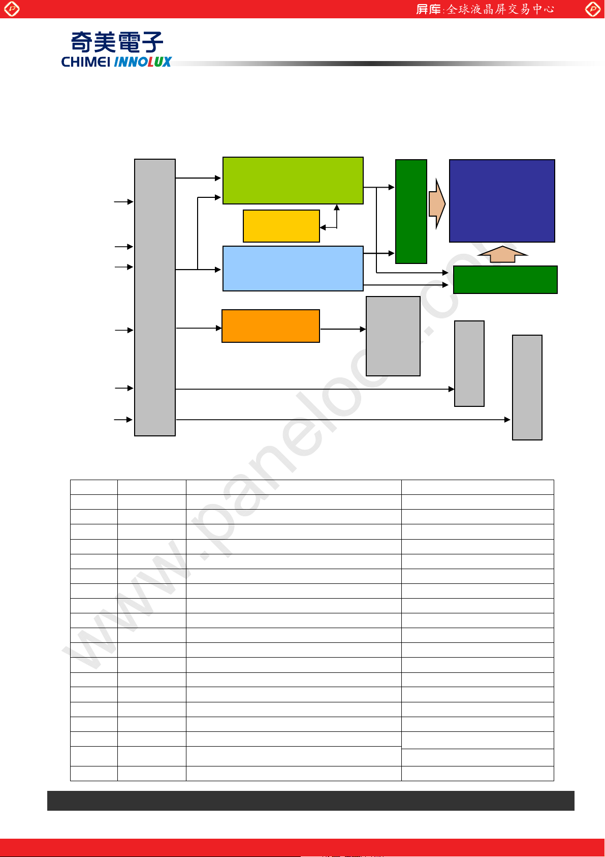
EDID
SCAN DRIVER IC
DC/DC CONVERTER &
LED
4. ELECTRICAL SPECIFICATIONS
4.1 FUNCTION BLOCK DIAGRAM
Display port
Signals
Converter
Input Signals
VCCS
GND
INPUT CONNECTOR
www.panelook.com
PRODUCT SPECIFICATION
DP INPUT /
TIMING CONTROLLER
EEPROM
REFERENCE VOLTAGE
GENERATOR
CONVERTER
TFT LCD PANEL
DATA DRIVER IC
LED Light-bar
Connector
TP Connector
CMOS Connector
TP Signals
CMOS Signals
4.2. INTERFACE CONNECTIONS
PIN ASSIGNMENT
Pin Symbol Description Remark
1 NC No Connection (Reserved)
2 H_GND High Speed Ground
3 LANE1_N Complement Signal Link Lane 1
4 LANE1_P True Signal Link Lane 1
5 H_GND High Speed Ground
6 LANE0_N Complement Signal Link Lane 0
7 LANE0_P True Signal Link Lane 0
8 H_GND High Speed Ground
9 AUX_CH_P True Signal Auxiliary Channel
10 AUX_CH_N Complement Signal Auxiliary Channel
11 H_GND High Speed Ground
12 VCCS Power Supply +3.3 V (typical)
13 VCCS Power Supply +3.3 V (typical)
14 BIST LCD Panel Self Test Enable
15 GND Ground
16 GND Ground
17 HPD Hot Plug Detect
18 BL_GND Backlight Ground
19 BL_GND Backlight Ground
Version 0.0 10 July 2012 8 / 26
copyright belongs to CHIMEI InnoLux. Any unauthorized use is prohibited.
One step solution for LCD / PDP / OLED panel application: Datasheet, inventory and accessory!
www.panelook.com
Page 9

Global LCD Panel Exchange Center
Pitch
20 BL_GND Backlight Ground
21 BL_GND Backlight Ground
22 LED_EN Backlight Enable Signal of LED Converter
23 LED_PWM
24 NC No Connection (Reserved)
25 NC No Connection (Reserved)
26 LED_VCCS Backlight Power
27 LED_VCCS Backlight Power
28 LED_VCCS Backlight Power
29 LED_VCCS Backlight Power
30 LOGO_VCCS LOGO LED Power Supply +5V, (typical)
Note (1) The first pixel is odd as shown in the following figure.
PWM Dimming Control Signal of LED
Converter
www.panelook.com
PRODUCT SPECIFICATION
1,1
(odd)
2,1
1,2
(even)
2,2
1,3
(odd)
1,4
(even)
1,Xmax
3,1
Pitch
Ymax,
Ymax,1
Xmax
Version 0.0 10 July 2012 9 / 26
copyright belongs to CHIMEI InnoLux. Any unauthorized use is prohibited.
One step solution for LCD / PDP / OLED panel application: Datasheet, inventory and accessory!
www.panelook.com
Page 10

Global LCD Panel Exchange Center
(High to Low)
SW Q2 C1
1K
C2
4.3 ELECTRICAL CHARACTERISTICS
4.3.1 LCD ELETRONICS SPECIFICATION
Parameter Symbol
Power Supply Voltage VCCS 3.0 3.3 3.6 V (1)-
www.panelook.com
PRODUCT SPECIFICATION
Val ue
Unit Note
Min. Typ. Max.
HPD
High Level 3.0 - 3.6 V
Low Level 0 - 0.4 V
Ripple Voltage VRP - 50 - mV (1)-
Inrush Current I
- - 1.5 A (1),(2)
RUSH
Mosaic (343) (376) mA (3)a
Power Supply Current
White
lcc
(408) (448) mA (3)b
Note (1) The ambient temperature is Ta = 25 ± 2 ºC.
Note (2) I
: the maximum current when VCCS is rising
RUSH
I
: the maximum current of the first 100ms after power-on
IS
Measurement Conditions: Shown as the following figure. Test pattern: black.
+3.3V
R1
47K
Q1 2SK1475
FUSE
C3
1uF
VCCS
(LCD Module Input)
(Control Signal)
+12V
VR1
R2
2SK1470
47K
1uF
0.01uF
VCCS rising time is 0.5ms
Version 0.0 10 July 2012 10 / 26
copyright belongs to CHIMEI InnoLux. Any unauthorized use is prohibited.
One step solution for LCD / PDP / OLED panel application: Datasheet, inventory and accessory!
www.panelook.com
Page 11

Global LCD Panel Exchange Center
Note (3) The specified power supply current is under the conditions at VCCS = 3.3 V, Ta = 25 ± 2 ºC, DC
www.panelook.com
PRODUCT SPECIFICATION
Current and f
a. Mosaic Pattern
= 60 Hz, whereas a power dissipation check pattern below is displayed.
v
b. White Pattern
Active Area
Active Area
Version 0.0 10 July 2012 11 / 26
copyright belongs to CHIMEI InnoLux. Any unauthorized use is prohibited.
One step solution for LCD / PDP / OLED panel application: Datasheet, inventory and accessory!
www.panelook.com
Page 12

Global LCD Panel Exchange Center
PWM Control Permissive Ripple
(High to Low)
C2
4.3.2 LED CONVERTER SPECIFICATION
Parameter Symbol
www.panelook.com
PRODUCT SPECIFICATION
Val ue
Unit Note
Min. Typ. Max.
Converter Input power supply voltage
Converter Inrush Current
LED_Vccs
ILED
RUSH
(7.0) 12.0 21.0 V
- - 1.5 A (1)
Backlight On 2.3 - 5.0 V
EN Control Level
Backlight Off
PWM High Level
PWM Control Level
PWM Low Level
0 - 0.5 V
2.3 - 5.0 V
0 - 0.5 V
10 - 100 %
PWM Control Duty Ratio
5 - 100 % (2)
Voltage
VPWM_pp
PWM Control Frequency f
LED Power Current LED_VCCS =Typ.
190 - 2K Hz (3)
PW M
ILED (293) (329) (429) mA (4)
- - 100 mV
Note (1) ILED
ILED
: the maximum current when LED_VCCS is rising,
RUSH
: the maximum current of the first 100ms after power-on,
IS
Measurement Conditions: Shown as the following figure. LED_VCCS = Typ, Ta = 25 ± 2 ºC, f
= 200 Hz, Duty=100%.
PW M
LED_VCCS(Typ)
Q1 IRL3303
R1
47K
FUSE
C3
1uF
(LED Conver ter Input )
(Control Signal)
SW= 24V
LED_VCCS(Typ)
R2
1K
47K
VR1
C1
1uF
0.01uF
Q2
IRL3303
Version 0.0 10 July 2012 12 / 26
copyright belongs to CHIMEI InnoLux. Any unauthorized use is prohibited.
One step solution for LCD / PDP / OLED panel application: Datasheet, inventory and accessory!
www.panelook.com
Page 13

Global LCD Panel Exchange Center
≤∗+
∗+≤
≥
www.panelook.com
PRODUCT SPECIFICATION
LED_VCC
LED_PWM
LED_EN
ILED
0V
0V
0V
ILED
VLED rising time is 0.5ms
0.5ms
90%
10%
Rush
100ms
ILED
IS
Note (2) If the PWM control duty ratio is less than 10%, there is some possibility that acoustic noise or
backlight flash can be found. And it is also difficult to control the brightness linearity.
Note (3) If PWM control frequency is applied in the range less than 1KHz, the “waterfall” phenomenon on
the screen may be found. To avoid the issue, it’s a suggestion that PWM control frequency should
follow the criterion as below.
PWM control frequency f
fN )33.0( f
: Integer )3(
N
should be in the range
PW M
fN
PW M
N
)66.0(
f : Frame rate
Note (4) The specified LED power supply current is under the conditions at “LED_VCCS = Typ.”, Ta = 25
± 2 ºC, f
= 200 Hz, Duty=100%.
PW M
Version 0.0 10 July 2012 13 / 26
copyright belongs to CHIMEI InnoLux. Any unauthorized use is prohibited.
One step solution for LCD / PDP / OLED panel application: Datasheet, inventory and accessory!
www.panelook.com
Page 14

Global LCD Panel Exchange Center
0V
VCM
|VID|
4.4 DISPLAY PORT SIGNAL TIMING SPECIFICATION
4.4.1 DISPLAY PORT INTERFACE
Parameter Symbol Min. Typ. Max. Unit Notes
Differential Signal Common Mode
Voltage(MainLink and AUX)
AUX AC Coupling Capacitor C
Note (1) Display port interface related AC coupled signals should follow VESA DisplayPort Standard
Version1. Revision 1a and VESA Embedded DisplayPort
(2) The AUX AC Coupling Capacitor should be placed on Source Devices.
(3)The source device should pass the test criteria described in DisplayPortCompliance Test
Specification (CTS) 1.1
www.panelook.com
PRODUCT SPECIFICATION
VCM 0 2 V (1)(3)
75 200 nF (2)
AUX
TM
Standard Version 1.1.
VD+
Single Ended
V
D-
Version 0.0 10 July 2012 14 / 26
The copyright belongs to CHIMEI InnoLux. Any unauthorized use is prohibited.
One step solution for LCD / PDP / OLED panel application: Datasheet, inventory and accessory!
www.panelook.com
Page 15

Global LCD Panel Exchange Center
4.5 DISPLAY TIMING SPECIFICATIONS
The input signal timing specifications are shown as the following table and timing diagram.
www.panelook.com
PRODUCT SPECIFICATION
Signal Item Symbol
DCLK Frequency 1/Tc (87.9) (138.5) (145.4) MHz -
Vertical Total Time TV (1104) (1112) (1120)
Vertical Active Display Period TVD 1080 1080 1080
DE
DE
Vertical Active Blanking Period TVB TV-TVD (32) TV-TVD TH -
Horizontal Total Time TH (2040) (2080) (2120)
Horizontal Active Display Period THD 1920 1920 1920
Horizontal Active Blanking Period THB
INPUT SIGNAL TIMING DIAGRAM
Min. Typ. Max.
TH-THD
(160)
TH-THD
Unit Note
TH -
TH -
Tc -
Tc -
Tc -
DCLK
DE
DATA
TC
T
HD
Version 0.0 10 July 2012 15 / 26
The copyright belongs to CHIMEI InnoLux. Any unauthorized use is prohibited.
One step solution for LCD / PDP / OLED panel application: Datasheet, inventory and accessory!
www.panelook.com
Page 16

Global LCD Panel Exchange Center
10%
t6
t9
-
-
-
4.6 POWER ON/OFF SEQUENCE
www.panelook.com
PRODUCT SPECIFICATION
-Power Supply
for LCD, VCCS
-eDP Display
-HPD from Sink
-AUX Channel
-Main Link Data
0V
0V
Power On
90%
10%
t1
Power Off
t11
90%
t2
Black Video
t3
AUX Channel Operational
t4
Link
Trainin g
Idle
t7
Valid Video Data
t10
Black Video Video from Source
Idle or off
Restart
10%
t12
Power Supply for
LED Converter,
LED_VCCS
LED Converter
Dimming Signal,
LED_PWM
LED Converter
Enable Signal,
LED_EN
0V
0V
0V
10%
t5
90%
t8
90%
10%
t
A
t
C
t
E
t
F
t
B
t
D
Version 0.0 10 July 2012 16 / 26
The copyright belongs to CHIMEI InnoLux. Any unauthorized use is prohibited.
One step solution for LCD / PDP / OLED panel application: Datasheet, inventory and accessory!
www.panelook.com
Page 17

Global LCD Panel Exchange Center
Timing Specifications:
Parameter
t1 Power rail rise time, 10% to 90%
t2
t3
t4
t5 Link training duration Source
t6 Link idle Source - - ms
t7
t8
t9
t10
t11
t12 VCCS Power off time Source 500 - ms
tA
tB
tC
tD
tE
tF
Note (1) Please don’t plug or unplug the interface cable when system is turned on.
Delay from LCD,VCCS to black
video generation
Delay from LCD,VCCS to HPD
high
Delay from HPD high to link
training initialization
Delay from valid video data from
Source to video on display
Delay from valid video data from
Source to backlight on
Delay from backlight off to end of
valid video data
Delay from end of valid video data
from Source to power off
VCCS power rail fall time, 90% to
10%
LED power rail rise time, 10% to
90%
LED power rail fall time, 90% to
10%
Delay from LED power rising to
LED dimming signal
Delay from LED dimming signal to
LED power falling
Delay from LED dimming signal to
LED enable signal
Delay from LED enable signal to
LED dimming signal
Description
www.panelook.com
PRODUCT SPECIFICATION
Reqd.
By
Source 0.5 10 ms -
Sink 0 200 ms -
Sink 0 200 ms -
Source - - ms
Sink 0 50 ms
Source
Source - - ms
Source 0 500 ms
Source 0.5 10 ms
Source 0.5 10 ms
Source 0 10 ms
Source 10 - ms
Source 10 - ms
Source 10 - ms -
Source 10 - ms -
Value
Min Max
- - ms
- - ms
Unit Notes
-
-
-
-
-
-
-
-
-
-
-
-
-
Note (2) Please avoid floating state of the interface signal during signal invalid period.
Note (3) It is recommended that the backlight power must be turned on after the power supply for LCD and the
interface signal is valid.
Version 0.0 10 July 2012 17 / 26
The copyright belongs to CHIMEI InnoLux. Any unauthorized use is prohibited.
One step solution for LCD / PDP / OLED panel application: Datasheet, inventory and accessory!
www.panelook.com
Page 18

Global LCD Panel Exchange Center
5. OPTICAL CHARACTERISTICS
5.1 TEST CONDITIONS
Item Symbol Value Unit
Ambient Temperature Ta
Ambient Humidity Ha
Supply Voltage VCC 3.3 V
Input Signal According to typical value in "3. ELECTRICAL CHARACTERISTICS"
LED Light Bar Input Current IL --- mA
The measurement methods of optical characteristics are shown in Section 5.2. The following items
should be measured under the test conditions described in Section 5.1 and stable environment shown in
Note (5).
5.2 OPTICAL SPECIFICATIONS
www.panelook.com
PRODUCT SPECIFICATION
o
25±2
50±10
C
%RH
The relative measurement methods of optical characteristics are shown as below. The following items
should be measured under the test conditions described in 5.1 and stable environment shown in Note (6).
Item Symbol
Rcx (0.664)
Rcy
Gcx (0.304)
Gcy
Bcx (0.142)
Bcy
Wcx
Color
Chromaticity
Red
Green
Blue
White
Wcy
Center Transmittance T%
Contrast Ratio CR
Response Time
Transmittance uniformity
Horizontal
Viewing Angle
Vertical
TR 14 19
T
F
δT%
θx+
θx-
θY+
θ
Y
Standard light source “C”
-
Condition Min. Typ. Max. Unit Note
-
(0.327)
-
-
=0°, θY =0°
θ
x
CS-2000T
=0°, θY =0°
θ
x
CS-2000T, CMO BLU
θ
=0°, θY =0°
x
=0°, θY =0°
θ
x
BM-5A
0.03
(0.591)
Typ +
0.03
Typ -
(0.088)
(0.333)
(0.363)
4.0 4.5
500
700
11 16
1.25 1.43
-
-
-
-
-
- (2), (3)
ms
ms
- (2),(6)
80 89
CR≥10
BM-5A
80 89
80 89
(2), (5)
80 89
Note (0) Light source is the standard light source “C” which is defined by CIE and driving voltages are
(0),(2),
(5),(8)
(1),(2),
(5),(7)
(4)
based on suitable gamma voltages. The calculating method is as followingΚ
1. Measure Module’s and BLU’s spectrums. White is without signal input and R, G, B are with
signal input. BLU is supplied by CMI.
2. Calculate cell’s spectrum.
3. Calculate cell’s chromaticity by using the spectrum of standard light source “C”
Note (1) Light source is the BLU which is supplied by CMI and driving voltages are based on suitable
gamma voltages. White is without signal input and R, G, B are with signal input. Spec is judged
by CMI’s golden sample.
Version 0.0 10 July 2012 18 / 26
The copyright belongs to CHIMEI InnoLux. Any unauthorized use is prohibited.
One step solution for LCD / PDP / OLED panel application: Datasheet, inventory and accessory!
www.panelook.com
Page 19

Global LCD Panel Exchange Center
T
ime
66.67 ms
66.67 ms
Note (2) Definition of Viewing Angle (θx, θy):
www.panelook.com
PRODUCT SPECIFICATION
θX- = 90º
x-
6 o’clock
θ
y-
= 90º
y-
Note (3) Definition of Contrast Ratio (CR):
The contrast ratio can be calculated by the following expression.
Contrast Ratio (CR) = L63 / L0
L63: Luminance of gray level 63
Normal
θx = θy = 0º
θy- θy+
θx−
θx+
y+
12 o’clock direction
θ
y+
= 90º
x+
θX+ = 90º
L 0: Luminance of gray level 0
CR = CR (1)
CR (X) is corresponding to the Contrast Ratio of the point X at Figure in Note (6).
Note (4) Definition of Response Time (T
100%
90%
Optical
Response
10%
0%
Note (5) Measurement Setup:
, TF):
R
T
R
TF
The LCD module should be stabilized at given temperature for 20 minutes to avoid abrupt
temperature change during measuring. In order to stabilize the luminance, the measurement
should be executed after lighting Backlight for 20 minutes in a windless room.
Version 0.0 10 July 2012 19 / 26
The copyright belongs to CHIMEI InnoLux. Any unauthorized use is prohibited.
One step solution for LCD / PDP / OLED panel application: Datasheet, inventory and accessory!
www.panelook.com
Page 20

Global LCD Panel Exchange Center
500 mm
LCD
P
anel
X=1 to 13
X
ʳ
www.panelook.com
PRODUCT SPECIFICATION
ʳ
LCD Module
ʳ
ʳ
ʳ
USB2000
ʳ
ʳ
ʳ
ʳ
Center of the Screen
Field of View = 2
ʳ
ʳ
ʳ
Note (6) Definition of Transmittance Variation (δT%):
Measure the transmittance at 5 points
ʳ
T% =
Maximum [T%(1), T%(2), … T%(5)]
Minimum [T%(1), T%(2), … T%(5)]
Note (7) Definition of Transmittance (T%):
Module is without signal input.
CS-2000T
º
Light Shield Room
(Ambient Luminance < 2 lux)
BLU is supplied by CMI.
Transmittance =
˄˃
˛˂ˇ
˛
˛˂ˇ ˛˂ˇ ˛˂ˇ
˄˃
ˉ
ˌ ˄˃
˄˄ ˄˅ ˄ˆ
˄˃ ˄˃
˪˂ˇ ˪˂ˇ ˪˂ˇ ˪˂ˇ
Note (8) The listed optical specifications refer to the initial value of manufacture, but the condition of
Luminance of LCD module
Ϡ 100%
Luminance of backlight
ˊ
˅ˆ
˄
ˇˈ
˪
ˋ
: Test Point
the specifications after long-term operation will not be warranted.
Version 0.0 10 July 2012 20 / 26
The copyright belongs to CHIMEI InnoLux. Any unauthorized use is prohibited.
One step solution for LCD / PDP / OLED panel application: Datasheet, inventory and accessory!
www.panelook.com
Page 21

Global LCD Panel Exchange Center
6. PACKING
6.1 CMI OPEN CELL LABEL
The barcode nameplate is pasted on each OPEN CELL as illustration for CMI internal control.
(a) Model Name: N133HSG - DJ1
www.panelook.com
PRODUCT SPECIFICATION
(b) Serial ID: X X
Serial ID includes the information as below:
(a) Manufactured Date: Year: 0~9, for 2010~2019
Day: 1~9, A~Y, for 1
(b) Revision Code: cover all the change
(c) Serial No.: Manufacturing sequence of product
X X X X X Y M D L N N N N
Month: 1~9, A~C, for Jan. ~ Dec.
Serial No.
Product Line
Year, Month, Date
CMI Internal Use
Revision
CMI Internal Use
st
to 31st, exclude I , O and U
(d) Product Line: 1 -> Line1, 2 -> Line 2, …etc.
Version 0.0 10 July 2012 21 / 26
The copyright belongs to CHIMEI InnoLux. Any unauthorized use is prohibited.
One step solution for LCD / PDP / OLED panel application: Datasheet, inventory and accessory!
www.panelook.com
Page 22

Global LCD Panel Exchange Center
6.2 PACKAGE RELIABILITY
(1) Carton Packing should have no failure in the following reliability test items
Test Item Test Conditions Note
ISTA STANDARD
Packing
Vibration
Random, Frequency Range: 1 – 200 Hz
Top & Bottom: 30 minutes (+Z), 10 min (-Z),
Right & Left: 10 minutes (X)
Back & Forth 10 minutes (Y)
6.3 CARTON
www.panelook.com
PRODUCT SPECIFICATION
Non Operation
Figure. 6-3 Packing method
Version 0.0 10 July 2012 22 / 26
The copyright belongs to CHIMEI InnoLux. Any unauthorized use is prohibited.
One step solution for LCD / PDP / OLED panel application: Datasheet, inventory and accessory!
www.panelook.com
Page 23

Global LCD Panel Exchange Center
6.4 PALLET
www.panelook.com
PRODUCT SPECIFICATION
Figure. 6-4 Packing method
Version 0.0 10 July 2012 23 / 26
The copyright belongs to CHIMEI InnoLux. Any unauthorized use is prohibited.
One step solution for LCD / PDP / OLED panel application: Datasheet, inventory and accessory!
www.panelook.com
Page 24

Global LCD Panel Exchange Center
7. PRECAUTIONS
7.1 HANDLING PRECAUTIONS
(1) The open cell should be assembled into the system firmly by using every mounting hole. Be careful
not to twist or bend the open cell.
(2) While assembling or installing open cell, it can only be in the clean area. The dust and oil may cause
electrical short or damage the polarizer.
(3) Use fingerstalls or soft gloves in order to keep display clean during the incoming inspection and
assembly process.
(4) Do not press or scratch the surface harder than a HB pencil lead on the panel because the polarizer
is very soft and easily scratched.
(5) If the surface of the polarizer is dirty, please clean it by some absorbent cotton or soft cloth. Do not
www.panelook.com
PRODUCT SPECIFICATION
use Ketone type materials (ex. Acetone), Ethyl alcohol, Toluene, Ethyl acid or Methyl chloride. It
might permanently damage the polarizer due to chemical reaction.
(6) Wipe off water droplets or oil immediately. Staining and discoloration may occur if they left on panel
for a long time.
(7) If the liquid crystal material leaks from the panel, it should be kept away from the eyes or mouth. In
case of contacting with hands, legs or clothes, it must be washed away thoroughly with soap.
(8) Protect the open cell from static electricity, it may cause damage to the C-MOS Gate Array IC.
(9) Do not disassemble the open cell.
(10) Pins of I/F connector should not be touched directly with bare hands.
7.2 STORAGE PRECAUTIONS
(1) High temperature or humidity may reduce the performance of open cell. Please store open cell
within the specified storage conditions.
(2) It is dangerous that moisture come into or contacted the open cell, because the moisture may
damage open cell when it is operating.
(3) It may reduce the display quality if the ambient temperature is lower than 10 ºC. For example, the
response time will become slowly.
7.3 OPERATION PRECAUTIONS
(1) Do not pull the I/F connector in or out while the open cell is operating.
(2) Always follow the correct power on/off sequence when open cell is connecting and operating. This
can prevent the CMOS LSI chips from damage during latch-up.
Version 0.0 10 July 2012 24 / 26
The copyright belongs to CHIMEI InnoLux. Any unauthorized use is prohibited.
One step solution for LCD / PDP / OLED panel application: Datasheet, inventory and accessory!
www.panelook.com
Page 25

Global LCD Panel Exchange Center
Appendix. EDID DATA STRUCTURE
The EDID (Extended Display Identification Data) data formats are to support displays as defined in the
VESA Plug & Display and FPDI standards.
TBD
Appendix. OUTLINE DRAWING
www.panelook.com
PRODUCT SPECIFICATION
Version 0.0 10 July 2012 25 / 26
The copyright belongs to CHIMEI InnoLux. Any unauthorized use is prohibited.
One step solution for LCD / PDP / OLED panel application: Datasheet, inventory and accessory!
www.panelook.com
Page 26

Global LCD Panel Exchange Center
www.panelook.com
PRODUCT SPECIFICATION
Version 0.0 10 July 2012 26 / 26
The copyright belongs to CHIMEI InnoLux. Any unauthorized use is prohibited.
One step solution for LCD / PDP / OLED panel application: Datasheet, inventory and accessory!
www.panelook.com
 Loading...