

Page 1
PRODUCT SPECIFICATION
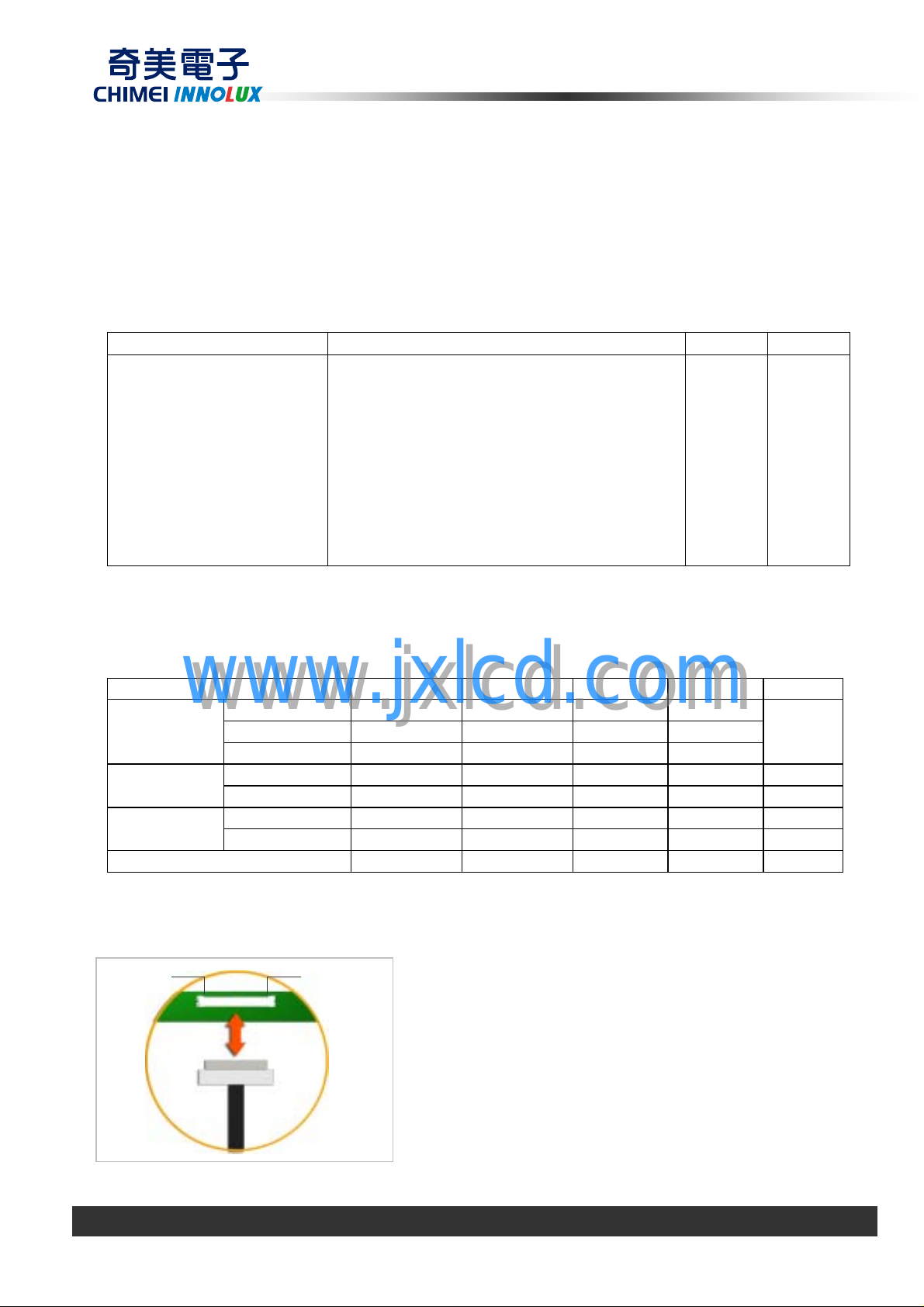
Doc. Number:
□ Tentative Specification
□ Preliminary Specification
■ Approval Specification
MODEL NO.: N101LGE
SUFFIX: P21
Customer: Toshiba
APPROVED BY SIGNATURE
www.jxlcd.com
www.jxlcd.com
Name / Title
Note
Please return 1 copy for your confirmation with your
signature and comments.
Approved By Checked By Prepared By
楊竣傑
2010-09-21
17:53:59
陳逸銘
2010-09-16
14:40:02
阮經綸
2010-09-15
13:31:53
Version 3.0 23 September 2010 1 / 25
The copyright belongs to CHIMEI InnoLux. Any unauthorized use is prohibited.
Page 2
PRODUCT SPECIFICATION
CONTENTS
1. GENERAL DESCRIPTION.........................................................................................................4
1.1 OVERVIEW ................................................................................................................................4
1.2 GENERAL SPECIFICATI0NS ...................................................................................................4
2. MECHANICAL SPECIFICATIONS .............................................................................................4
2.1 CONNECTOR TYPE..................................................................................................................4
3. ABSOLUTE MAXIMUM RATINGS.............................................................................................5
3.1 ABSOLUTE RATINGS OF ENVIRONMENT ..........................................................................5
3.2 ELECTRICAL ABSOLUTE RATINGS......................................................................................6
3.2.1 TFT LCD MODULE...............................................................................................6
4. ELECTRICAL SPECIFICATIONS...............................................................................................7
4.1 FUNCTION BLOCK DIAGRAM...............................................................................................7
4.2 INTERFACE CONNECTIONS ..................................................................................................7
4.2.1 LVDS INPUT PIN ASSIGNMENT..........................................................................7
4.2.2 LED CONVERTER OUTPUT PIN ASSIGNMENT.................................................8
4.3 ELECTRICAL CHARACTERISTICS........................................................................................9
4.3.1 LCD ELETRONICS SPECIFICATION...................................................................9
4.3.2 LED CONVERTER SPECIFICATION .................................................................11
4.3.3 LED CONVERTER OUTPUT RATINGS .............................................................12
4.4 LVDS INPUT SIGNAL TIMING SPECIFICATIONS .............................................................13
4.5 DISPLAY TIMING SPECIFICATIONS ...................................................................................15
4.6 POWER ON/OFF SEQUENCE ................................................................................................16
5. OPTICAL CHARACTERISTICS (light source: C light) ..........................................................17
6. RELIABILITY TEST ITEM ........................................................................................................20
7. PACKING..................................................................................................................................21
7.1 CARTON LABEL .....................................................................................................................21
7.2 CARTON...................................................................................................................................22
www.jxlcd.com
www.jxlcd.com
4.4.1 LVDS DC SPECIFICATIONS..............................................................................13
4.4.2 LVDS DATA FORMAT.........................................................................................13
4.4.3 COLOR DATA INPUT ASSIGNMENT.................................................................14
7.3 PALLET.....................................................................................................................................23
8. PRECAUTIONS........................................................................................................................24
8.1 HANDLING PRECAUTIONS..................................................................................................24
8.2 STORAGE PRECAUTIONS ....................................................................................................24
8.3 OPERATION PRECAUTIONS.................................................................................................24
Appendix. OUTLINE DRAWING..................................................................................................25
Version 3.0 23 September 2010 2 / 25
The copyright belongs to CHIMEI InnoLux. Any unauthorized use is prohibited.
Page 3
PRODUCT SPECIFICATION
REVISION HISTORY
Version Date Page Description
3.0 Sep.15, 2010 All Spec Ver.3.0 was first issued.
www.jxlcd.com
www.jxlcd.com
Version 3.0 23 September 2010 3 / 25
The copyright belongs to CHIMEI InnoLux. Any unauthorized use is prohibited.
Page 4
PRODUCT SPECIFICATION
1. GENERAL DESCRIPTION
1.1 OVERVIEW
N101LGE-P21 is a 10.1” (10.06” diagonal) TFT Liquid Crystal Display cell with driver ICs and a
40-pin-and-1ch-LVDS circuit board. This product supports 1024 x 600 WXGA mode and can
display 262,144 colors. T
direction.
1.2 GENERAL SPECIFICATI0NS
Item Specification Unit Note
Screen Size 10.06” diagonal
Driver Element a-si TFT active matrix - Pixel Number 1024 x R.G.B. x 600 pixel Pixel Pitch 0.2175 (H) x 0.2088 (V) mm Pixel Arrange ment RGB vertical stripe - Display Colors 262,144 color Transmissive Mode Normally white - Surface Treat ment Hard coating (3H), Glare - -
Power Consumption Cell 0.561 W (Max.)
Note (1) The specified power consumption (with converter efficiency) is under the conditions at VCCS =
3.3 V, fv = 60 Hz, Ta = 25 ± 2 ºC, whereas mosaic pattern is displayed.
2. MECHANICAL SPECIFICATIONS
Item Min. Typ. Max. Unit Note
www.jxlcd.com
www.jxlcd.com
Horizontal (H) 231.15 231.45 231.75 mm
Module Size
Bezel Area
Active Area
Note (1) Please refer to the attached drawings for more information of front and back outline dimensions.
Vertical (V) 170.8 171.1 171.4 mm
Thickness (T) - 1.27 1.4 mm
Horizontal
Vertical
Horizontal - 222.72 - mm
Vertical - 125.28 - mm
Weight - 92.3 97.3 g
he backlight unit is not built in. The optimum viewing angle is at 6 o’clock
(1)
(1)
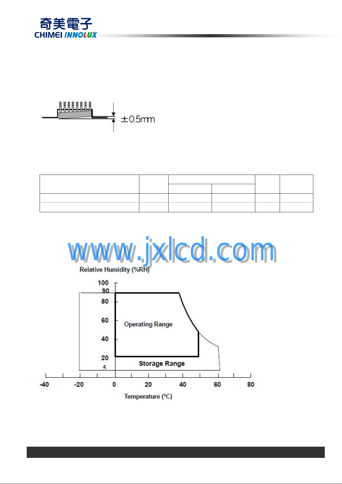
2.1 CONNECTOR TYPE
Version 3.0 23 September 2010 4 / 25
The copyright belongs to CHIMEI InnoLux. Any unauthorized use is prohibited.
Pin1 Pin40
Page 5
PRODUCT SPECIFICATION
Please refer Appendix Outline Drawing for detail design.
Connector Part No.: IPEX-20455-040E-12 or Tyco 5-2069716-3 ,or equivalent
User’s connector Part No: IPEX-20453-040T-01 or equivalent
Note (1) Mounting inclination of a connector carries out as follows
3. ABSOLUTE MAXIMUM RATINGS
3.1 ABSOLUTE RATINGS OF ENVIRONMENT
Item Symbol
Min. Max.
Storage Temperature TST -20 +60 ºC (1)
Operating Ambient T emperature TOP 0 +50 ºC (1), (2)
Value
Unit Note
Note (1) (a) 90 %RH Max. (Ta <= 40 ºC).
(b) Wet-bulb temperature should be 39 ºC Max. (Ta > 40 ºC).
(c) No condensation.
Note (2) The temperature of panel surface should be 0 ºC min. and 60 ºC max.
www.jxlcd.com
www.jxlcd.com
Version 3.0 23 September 2010 5 / 25
The copyright belongs to CHIMEI InnoLux. Any unauthorized use is prohibited.
Page 6
PRODUCT SPECIFICATION
3.2 ELECTRICAL ABSOLUTE RATINGS
3.2.1 TFT LCD MODULE
Item Symbol
Power Supply V oltage VCCS -0.3 +4.0 V
Logic Input Voltage VIN -0.3 VCCS+0.3 V
Converter Input Voltage
Converter Control Signal Voltage
Converter Control Signal Voltage
Note (1) Stresses beyond those listed in above “ELECTRICAL ABSOLUTE RATINGS” may cause
permanent damage to the device. Normal operation should be restricted to the conditions
described in “ELECTRICAL CHARACTERISTICS”.
LED_VCCS
LED_PWM,
LED_EN
Value
Min. Max.
-0.3 25 V (1)
-0.3 5 V (1)
-0.3 5 V (1)
Unit Note
(1)
www.jxlcd.com
www.jxlcd.com
Version 3.0 23 September 2010 6 / 25
The copyright belongs to CHIMEI InnoLux. Any unauthorized use is prohibited.
Page 7
4. ELECTRICAL SPECIFICATIONS
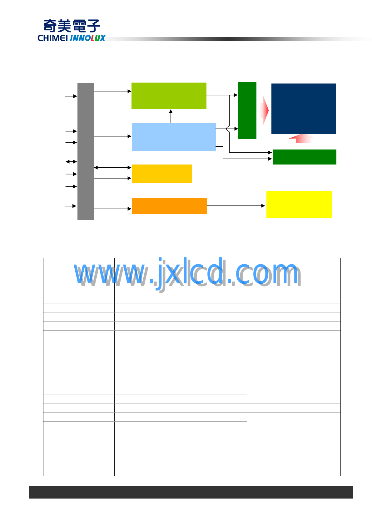
4.1 FUNCTION BLOCK DIAGRAM
LVDS Display
Data & Clock
Data
CLK
V
VCCS
GND
EDID
EDID
EDID
INPUT CONNECTOR
TIMING ONTROLLER
DC/DC CONVERTER &
REFERENCE VOLTAGE
PRODUCT SPECIFICATION
SCAN DRIVER IC
TFT LCD
PANEL
GENERATOR
DA TA DRIVER IC
EDID
EEPROM
Converter
Input Signals
4.2 INTERFACE CONNECTIONS
4.2.1 LVDS INPUT PIN ASSIGNMENT
Pin Symbol Description Remark
1 NC No Connection (Reserve)
2 VCCS Power Supply (3.3V typ.)
www.jxlcd.com
3 VCCS Power Supply (3.3V typ.)
4 VEDID DDC 3.3V power
5 NC No Connection (Reserved for CMI test)
6 CLKEDID DDC clock
7 DATAEDID DDC data
8 Rxin0- LVDS differential data input
9 Rxin0+ LVDS differential data input
10 VSS Ground
11 Rxin1- LVDS differential data input
12 Rxin1+ LVDS differen tial data input
13 VSS Ground
14 Rxin2- LVDS Differential Data Input
15 Rxin2+ LVDS Differential Data Input
16 VSS Ground
17 RxCLK- LVDS differential clock input
18 RxCLK+ LVDS differential clock input
19 VSS Ground
20 NC No Connection (Reserve)
21 NC No Connection (Reserve)
22 VSS Ground
23 NC No Connection (Reserve)
www.jxlcd.com
LED CONVERTER
LED CONVERTER
OUTPUT PAD
R0-R5, G0
G1~G5, B0, B1
B2-B5,HS,VS, DE
LVDS CLK
Version 3.0 23 September 2010 7 / 25
The copyright belongs to CHIMEI InnoLux. Any unauthorized use is prohibited.
Page 8
PRODUCT SPECIFICATION
24 NC No Connection (Reserve)
25 VSS Ground
26 NC No Connection (Reserve)
27 NC No Connection (Reserve)
28 VSS Ground
29 NC No Connection (Reserve)
30 NC No Connection (Reserve)
31 LED_GND LED Ground
32 LED_GND LED Ground
33 LED_GND LED Ground
34 NC No Connection (Reserve)
35 LED_PWM PWM Control Signal of LED Converter
36 LED_EN Enable Control Signal of LED Converter
37 NC No Connection (Reserve)
38 LED_VCCS LED Power Supply
39 LED_VCCS LED Power Supply
40 LED_VCCS LED Power Supply
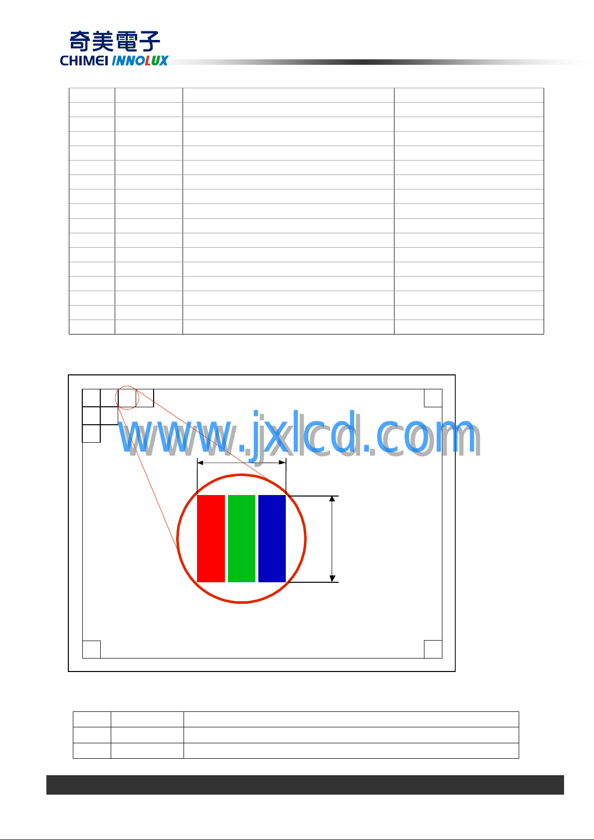
Note (1) The first pixel is odd as shown in the following figure.
1,1
(odd)
2,1
3,1
1,2
1,3
(even)
(odd)
2,2
www.jxlcd.com
www.jxlcd.com
1,4
(even)
Pitch
Pitch
Ymax,1
1,Xmax
Ymax,
Xmax
4.2.2 LED CONVERTER OUTPUT PIN ASSIGNMENT
Pin Symbol Description
1 VL LED converter output voltage
2 ICH LED converter feedback channel
Version 3.0 23 September 2010 8 / 25
The copyright belongs to CHIMEI InnoLux. Any unauthorized use is prohibited.
Page 9

PRODUCT SPECIFICATION
4.3 ELECTRICAL CHARACTERISTICS
4.3.1 LCD ELETRONICS SPECIFICATION
Parameter Symbol
Min. Typ. Max.
Power Supply V oltage VCCS 3.0 3.3 3.6 V Ripple Voltage VRP - 50 - mV -
Value
Unit Note
Inrush Current I
- - 1.5 A (2)
RUSH
Mosaic - 150 170 mA (3)a
Power Supply Current
Black
lcc
- 160 180 mA (3)b
Note (1) The ambient temperature is Ta = 25 ± 2 ºC.
Note (2) I
: the maximum current when VCCS is rising
RUSH
I
: the maximum current of the first 100ms after power-on
IS
Measurement Conditions: Shown as the following figure. Test pattern: black.
+3.3V
Q1 2SK1475
VR1
R1
47K
Q2
2SK1470
C2
47K
R2
1K
0.01uF
(High to Low)
(Control Signal)
SW
+12V
www.jxlcd.com
www.jxlcd.com
C1
1uF
FUSE
C3
1uF
VCCS
(LCD Module Input)
VCCS rising time is 0.5ms
Version 3.0 23 September 2010 9 / 25
The copyright belongs to CHIMEI InnoLux. Any unauthorized use is prohibited.
Page 10

PRODUCT SPECIFICATION
Note (3) The specified power supply current is under the conditions at VCCS = 3.3 V, Ta = 25 ± 2 ºC, DC
Current and f
a. Mosaic Pattern
= 60 Hz, whereas a power dissipation check pattern below is displayed.
v
b. Black Pattern
Active Area
Active Area
www.jxlcd.com
www.jxlcd.com
Version 3.0 23 September 2010 10 / 25
The copyright belongs to CHIMEI InnoLux. Any unauthorized use is prohibited.
Page 11

PRODUCT SPECIFICATION
4.3.2 LED CONVERTER SPECIFICATION
Parameter Symbol
Value
Unit Note
Min. Typ. Max.
Converter Input power supply voltage
Converter Inrush Current
LED_Vccs
ILED
RUSH
6.0 12.0 21.0 V
- - 1.5 A (1)
Backlight On 2.3 - 5 V
EN Control Level
Backlight Off
0 - 0.5 V
PWM High Level 2.3 - 5 V
PWM Control Level
PWM Low Level
0 - 0.5 V
PWM Control Duty Ratio 5 - 100 %
PWM Control Permissive Ripple
Voltage
PWM Control Frequency f
Note (1) ILED
ILED
: the maximum current when LED_VCCS is rising,
RUSH
: the maximum current of the first 100ms after power-on,
IS
VPWM_pp
190 - 2K Hz (2)
PWM
- - 100 mV
Measurement Conditions: Shown as the following figure. LED_VCCS = Typ, Ta = 25 ± 2 ºC, f
= 200 Hz, Duty=100%.
www.jxlcd.com
www.jxlcd.com
LED_VCCS(Typ)
Q1 IRL3303
VR1
R1
47K
R2
1K
47K
0.01uF
Q2
IRL3303
C2
(High to Low)
(Control Signal)
SW=24V
LED_VCCS(Typ)
C1
1uF
FUSE
C3
1uF
(LED Converter Input)
PWM
Version 3.0 23 September 2010 11 / 25
The copyright belongs to CHIMEI InnoLux. Any unauthorized use is prohibited.
Page 12

PRODUCT SPECIFICATION
≤
∗
∗+≤
LED_VCC
LED_PWM
LED_EN
ILED
0V
0V
0V
ILED
VLED rising time is 0.5ms
0.5ms
90%
10%
Rush
100ms
ILED
IS
Note (2) If PWM control frequency is applied in the range less than 1KHz, the “waterfall” phenomenon on
the screen may be found. To avoid the issue, it’s a suggestion that PWM control frequency should
www.jxlcd.com
www.jxlcd.com
follow the criterion as below.
PWM control frequency f
+ fN )33.0( f
should be in the range
PWM
fN
PWM
)66.0(
N : Integer )3( ≥N
f : Frame rate
4.3.3 LED CONVERTER OUTPUT RATINGS
Parameter Symbol
V
Converter output voltage
Converter output current
Converter feedback channel current ICH 38 40 42 mA
L
I
L
Min. Typ. Max.
21 - 34 V
38 40 42 mA
Value
Unit Note
Version 3.0 23 September 2010 12 / 25
The copyright belongs to CHIMEI InnoLux. Any unauthorized use is prohibited.
Page 13

PRODUCT SPECIFICATION
|
|
4.4 LVDS INPUT SIGNAL TIMING SPECIFICATIONS
4.4.1 LVDS DC SPECIFICATIONS
Parameter Symbol
Min. Typ. Max.
LVDS Differential Input High Threshold V
LVDS Differential Input Low Threshold V
LVDS Common Mode Voltage VCM 1.125 - 1.375 V (1)
LVDS Differential Input Voltage |VID| 100 - 600 mV (1)
L VDS Terminating Resistor RT - 100 - Ohm -
Note (1) The parameters of LVDS signals are defined as the following figures.
Single Ended
CM
V
0V
TH(LVDS)
-100 - - mV
TL(LVDS)
- - +100 mV
Value
Unit Note
V
CM
V
CM
VID|
(1),
=1.2V
(1)
=1.2V
www.jxlcd.com
www.jxlcd.com
Differential
4.4.2 LVDS DATA FORMAT
CLK+
Rxin2
Rxin1
Rxin0
T/7
IN20 IN19 IN18 IN17 IN16 IN15 IN14
DE B5 B4 B3 B2 Vsync Hsync
IN13 IN12 IN11 IN10 IN9 IN8 IN7
B1 G4 G3 G2 G1 B0 G5
IN6
G0 R3 R2 R1 R0
V
0V
V
IN5 IN4 IN3 IN2 IN1 IN0
R5
VID|
R4
Signal for 1 DCLK Cycle (T)
Version 3.0 23 September 2010 13 / 25
The copyright belongs to CHIMEI InnoLux. Any unauthorized use is prohibited.
Page 14

PRODUCT SPECIFICATION
4.4.3 COLOR DATA INPUT ASSIGNMENT
The brightness of each primary color (red, green and blue) is based on the 6-bit gray scale data input
for the color. The higher the binary input the brighter the color. The table below provides the assignment
of color versus data input.
Data Signal
Color
R5 R4 R3 R2 R1 R0 G5 G4 G3 G2 G1 G0 B5 B4 B3 B2 B1 B0
Black
Red
Green
Basic
Colors
Gray
Scale
Of
Red
Gray
Scale
Of
Green
Gray
Scale
Of
Blue
Note (1) 0: Low Level Voltage, 1: High Level Voltage
Blue
Cyan
Magenta
Yellow
White
Red(0)/Dark
Red(1)
Red(2)
:
:
Red(61)
Red(62)
Red(63)
Green(0)/Dark
Green(1)
Green(2)
:
:
Green(61)
www.jxlcd.com
www.jxlcd.com
Green(62)
Green(63)
Blue(0)/Dark
Blue(1)
Blue(2)
:
:
Blue(61)
Blue(62)
Blue(63)
0
1
0
0
0
1
1
1
0
0
0
:
:
1
1
1
0
0
0
:
:
0
0
0
0
0
0
:
:
0
0
0
Red Green Blue
0
0
0
0
0
0
0
0
0
0
0
0
0
0
0
0
1
1
1
1
1
0
0
0
0
0
0
0
0
0
0
0
0
0
0
0
0
1
1
1
1
1
1
0
0
0
0
0
0
0
0
0
0
0
0
0
0
0
0
1
1
1
1
1
0
0
0
0
0
1
1
1
1
1
1
1
1
1
1
1
1
1
1
1
1
0
0
0
0
0
0
1
1
1
1
1
1
1
1
1
1
1
1
1
1
1
1
0
0
0
0
0
1
1
1
1
1
1
1
1
1
1
1
1
1
1
1
1
0
0
0
0
0
0
0
0
0
0
0
0
0
0
0
0
0
0
0
0
1
0
0
0
0
0
0
0
0
0
0
0
0
0
0
1
0
0
0
0
0
0
0
0
0
0
0
0
:
:
:
:
:
:
:
:
:
:
:
:
:
:
:
:
:
:
:
:
:
:
:
:
:
:
:
:
:
:
:
:
1
1
1
0
1
0
0
0
0
0
0
0
0
0
0
0
1
1
1
1
0
0
0
0
0
0
0
0
0
0
0
0
1
1
1
1
1
0
0
0
0
0
0
0
0
0
0
0
0
0
0
0
0
0
0
0
0
0
0
0
0
0
0
0
0
0
0
0
0
0
0
0
0
0
1
0
0
0
0
0
0
0
0
0
0
0
0
0
0
1
0
0
0
0
0
0
:
:
:
:
:
:
:
:
:
:
:
:
:
:
:
:
:
:
:
:
:
:
:
:
:
:
:
:
:
:
:
:
0
0
0
0
0
1
1
1
1
0
1
0
0
0
0
0
0
0
0
0
0
1
1
1
1
1
0
0
0
0
0
0
0
0
0
0
0
1
1
1
1
1
1
0
0
0
0
0
0
0
0
0
0
0
0
0
0
0
0
0
0
0
0
0
0
0
0
0
0
0
0
0
0
0
0
0
0
0
0
0
0
0
0
0
0
0
0
0
0
0
0
0
0
0
0
1
:
:
:
:
:
:
:
:
:
:
:
:
:
:
:
:
:
:
:
:
:
:
:
:
:
:
:
:
:
:
:
:
0
0
0
0
0
0
0
0
0
0
0
1
1
1
1
0
0
0
0
0
0
0
0
0
0
0
0
1
1
1
1
1
0
0
0
0
0
0
0
0
0
0
0
1
1
1
1
1
0
0
0
1
1
1
0
1
0
0
0
:
:
0
0
0
0
0
0
:
:
0
0
0
0
1
0
:
:
1
0
1
Version 3.0 23 September 2010 14 / 25
The copyright belongs to CHIMEI InnoLux. Any unauthorized use is prohibited.
Page 15

PRODUCT SPECIFICATION
4.5 DISPLAY TIMING SPECIFICATIONS
The input signal timing specifications are shown as the following table and timing diagram.
Signal Item Symbol Min. Typ. Max. Unit Note
DCLK Frequency 1/Tc 39.57 43.97 46.16 MHz -
Vertical Total Time TV 604 619 624 TH -
Vertical Active Display Period TVD 600 600 600 TH -
DE
Note (1) Because this module is operated by DE only mode, Hsync and Vsync are ignored.
DE
DCLK
DE
Vertical Active Blanking Period TVB TV-TVD 19 TV-TVD TH -
Horizontal Total Time TH 1 106 1184 1224 Tc -
Horizontal Active Display Period THD 1024 1024 1024 Tc -
Horizontal Active Blanking Period THB
INPUT SIGNAL TIMING DIAGRAM
www.jxlcd.com
www.jxlcd.com
TC
TH-THD
T
HD
160
TH-THD
Tc -
DATA
Version 3.0 23 September 2010 15 / 25
The copyright belongs to CHIMEI InnoLux. Any unauthorized use is prohibited.
Page 16

PRODUCT SPECIFICATION
4.6 POWER ON/OFF SEQUENCE
The power sequence specifications are shown as the following table and diagram.
Symbol
t1 0.5 - 10 ms
t2 0 - 50 ms
t3 0 - 50 ms
t4 500 - - ms
t5 200 - - ms
t6 200 - - ms
t7 0.5 - 10 ms
tA 0.5 - 10 ms
tB 0 10 ms
tC 10 - - ms
tD 10 - - ms
tE 10 - - ms
tF 10 - - ms
Min. Typ. Max.
Value
Unit Note
- Power Supply
for LCD, VCCS
- Interface Signal
(LVDS Signal of
Transmitter), VI
- Power Supply for
LED Converter,
LED_VCCS
- LED Converter
Dimming Signal,
LED_PWM
- LED Converter
Enable Signal,
LED_EN
Power On
90%
10%
0V
www.jxlcd.com
www.jxlcd.com
0V
0V
0V
0V
Power Off
t1
t2
Valid Data
t6 t5
90%
10%
tA
tC
PWM Signal
tE t
90%
tB
t
D
F
t7
90%
10%
t3
10%
10%
t4
Note (1) Please don’t plug the interface cable of on when sy stem is turned on.
Note (2) Please avoid floating state of the interface signal during signal invalid period.
Note (3) It is recommended that the backlight power must be turned on after the power supply for LCD and the
interface signal is valid.
Version 3.0 23 September 2010 16 / 25
The copyright belongs to CHIMEI InnoLux. Any unauthorized use is prohibited.
Page 17

PRODUCT SPECIFICATION
5. OPTICAL CHARACTERISTICS (light source: C light)
Item Symbol Conditions
Transmittance T% -- 7.05 -- %
Contrast Ratio CR 400 500 -- -
Response Time
Hor.
Viewing Angle
Ver.
Red
Green
Chromaticity
Blue
White
TR -- 3 8 ms
T
θ
X+
θ
X-
θ
Y+
θ
Y-
Rx 0.562 0.592 0.622 Ry 0.316 0.346 0.376 Gx 0.270 0.300 0.330 Gy 0.517 0.547 0.577 Bx 0.112 0.142 0.172 -
By 0.153 0.183 0.213 Wx 0.284 0.314 0.344 Wy
F
Viewing
normal
angle θ
=0°
θ
Y
Center
CR≥10
=
X
Specifications
Min. Typ. Max.
-- 7 12 ms
40 45 -40 45 -15 20 --
40 45 --
0.329 0.359 0.389 -
Unit Note
deg.
All left side data are based on
CMI’s following condition
1. Color Gamut: NTSC 43.7%
2. LC: TN
3. Light Source: CMI LED
BLU
4. Film: Sumitomo
SRW062APK/SRW062APK
dark < 5 V, VLC white <1 V
5. V
LC
Simulation Data
Reference Only
Under C light simulation
Note (1) Definition of Contrast Ratio (CR):
The contrast ratio can be calculated by the following expression.
Contrast Ratio (CR) = L63 / L0
www.jxlcd.com
www.jxlcd.com
L63: Luminance of gray level 63
L 0: Luminance of gray level 0
CR = CR (5)
CR (X) is corresponding to the Contrast Ratio of the point X at Figure in Note (5).
Note (2) Definition of Response Time (
TR, TF):
100%
90%
Optical
Response
10%
0%
T
T
R
F
Time
Version 3.0 23 September 2010 17 / 25
The copyright belongs to CHIMEI InnoLux. Any unauthorized use is prohibited.
Page 18

Note(3) Definition of Viewing Angle
(
A
)
θ
θx− θx+
θ
θ
y
PRODUCT SPECIFICATION
Normal
x =
= 0º
y-
x-
Note (4) Measurement Set-Up:
The LCD module should be stabilized at a given temperature for 20 minutes to avoid abrupt temperature
change during measuring. In order to stabilize the luminance, the measurement should be executed after lighting
Backlight for 20 minutes in a windless room.
θX- = 90º
6 o’clock
θ
y- = 90º
www.jxlcd.com
www.jxlcd.com
LCD M odule
θy- θy+
12 o’clock direction
y+
y+ = 90º
x+
θX+ = 90º
LCD P anel
USB2000
Center of the S creen
Version 3.0 23 September 2010 18 / 25
or equivalent
500 mm
or equivalent
CS-2000T
Light Shield Room
mbient Luminance < 2 l u x
The copyright belongs to CHIMEI InnoLux. Any unauthorized use is prohibited.
Page 19

Note (5) Definition of White Variation (δW):
Measure the luminance of gray level 63 at 5 points
= {Minimum [L (1) ~ L (5)] / Maximum [L (1) ~ L (5)]}*100%
δW
5p
PRODUCT SPECIFICATION
Note (6) The listed optical specifications refer to the initial value of manufacture, but the condition of the
specifications after long-term operation will not be warranted.
www.jxlcd.com
www.jxlcd.com
Version 3.0 23 September 2010 19 / 25
The copyright belongs to CHIMEI InnoLux. Any unauthorized use is prohibited.
Page 20

PRODUCT SPECIFICATION
6. RELIABILITY TEST ITEM
Test Item Test Condition Note
High Temperature S t orage Test 60ºC, 240 hours
Low Temperature Storage Test -20ºC, 240 hours
Thermal Shock Storage Test
-20ºC, 0.5hour←→60℃, 0.5hour; 100cycles, 1hour/cycle
High Temperature Operation Test 50ºC, 240 hours
Low Temperature Operation Test 0ºC, 240 hours
High Temperature & High Humidity
Operation Test
Note (1) criteria : Normal display image with no obvious non-uniformity and no line defect.
Note (2) Evaluation should be tested after storage at room temperature for more than two hour
www.jxlcd.com
www.jxlcd.com
50ºC, RH 80%, 240hours
(1) (2)
Version 3.0 23 September 2010 20 / 25
The copyright belongs to CHIMEI InnoLux. Any unauthorized use is prohibited.
Page 21

7. PACKING
7.1 CARTON LABEL
PRODUCT SPECIFICATION
N101LGE-P21
XX
Made in XXXX
Production location: Made In XXXX. XXXX stands for production location.
www.jxlcd.com
www.jxlcd.com
Version 3.0 23 September 2010 21 / 25
The copyright belongs to CHIMEI InnoLux. Any unauthorized use is prohibited.
Page 22

7.2 CARTON
PRODUCT SPECIFICATION
www.jxlcd.com
www.jxlcd.com
Figure. 7-1 Packing
Version 3.0 23 September 2010 22 / 25
The copyright belongs to CHIMEI InnoLux. Any unauthorized use is prohibited.
Page 23

7.3 PALLET
PRODUCT SPECIFICATION
www.jxlcd.com
www.jxlcd.com
Figure. 7-2 Packing
Version 3.0 23 September 2010 23 / 25
The copyright belongs to CHIMEI InnoLux. Any unauthorized use is prohibited.
Page 24

PRODUCT SPECIFICATION
8. PRECAUTIONS
8.1 HANDLING PRECAUTIONS
(1) The module should be assembled into the system firmly by using every mounting hole. Be careful
not to twist or bend the module.
(2) While assembling or installing modules, it can only be in the clean area. The dust and oil may cause
electrical short or damage the polarizer.
(3) Use fingerstalls or soft gloves in order to keep display clean during the incoming inspection and
assembly process.
(4) Do not press or scratch the surface harder than a HB pencil lead on the panel because the polarizer
is very soft and easily scratched.
(5) If the surface of the polarizer is dirty, please clean it by some absorbent cotton or soft cloth. Do not
use Ketone type materials (ex. Acetone), Ethyl alcohol, Toluene, Ethyl acid or Methyl chloride. It
might permanently damage the polarizer due to chemical reaction.
(6) Wipe off water droplets or oil immediately. Staining and discoloration may occur if they left on panel
for a long time.
(7) If the liquid crystal material leaks from the panel, it should be kept away from the eyes or mouth. In
case of contacting with hands, legs or clothes, it must be washed away thoroughly with soap.
(8) Protect the module from static electricity, it may cause damage to the C-MOS Gate Array IC.
(9) Do not disassemble the module.
(10) Do not pull or fold the LED wire.
www.jxlcd.com
(11) Pins of I/F connector should not be touched directly with bare hands.
8.2 STORAGE PRECAUTIONS
(1) High temperature or humidity may reduce the performance of module. Please store LCD module
within the specified storage conditions.
(2) It is dangerous that moisture come into or contacted the LCD module, because the moisture may
damage LCD module when it is operating.
(3) It may reduce the display quality if the ambient temperature is lower than 10 ºC. For example, the
response time will become slowly, and the starting voltage of LED will be higher than the room
temperature.
www.jxlcd.com
8.3 OPERATION PRECAUTIONS
(1) Do not pull the I/F connector in or out while the module is operating.
(2) Always follow the correct power on/off sequence when LCD module is connecting and operating.
This can prevent the CMOS LSI chips from damage during latch-up.
(3) The startup voltage of Backlight is approximately 1000 Volts. It may cause electrical shock while
assembling with converter . Do not disassemble the module or insert anything into the Backlight unit.
Version 3.0 23 September 2010 24 / 25
The copyright belongs to CHIMEI InnoLux. Any unauthorized use is prohibited.
Page 25

Appendix. OUTLINE DRAWING
PRODUCT SPECIFICATION
www.jxlcd.com
www.jxlcd.com
Version 3.0 23 September 2010 25 / 25
The copyright belongs to CHIMEI InnoLux. Any unauthorized use is prohibited.
 Loading...