

CHIMEI V420H1 User Guide
Issue Date: Dec.18.2006
A
Model No.:V420H1-L07
Approval
TFT LCD Approval Specification
MODEL NO.: V420H1 - L07
Customer:
pproved by:
Note:
Approved By
Reviewed By
TV Head Division.
LY Chen
QRA Dept. Product Development Div.
Tomy Chen WT Lin
Prepared By
LCD TV Marketing and Product Management Div.
Ken Wu Menghui Lin
1
Issue Date: Dec.21.2006
Model No.:V420H1-L07
Approval
- CONTENTS -
1. GENERAL DESCRIPTION -------------------------------------------------------4
1.1 OVERVIEW
1.2 FEATURES
1.3 APPLICATION
1.4 GENERAL SPECIFICATIONS
1.5 MECHANICAL SPECIFICATIONS
2. ABSOLUTE MAXIMUM RATINGS
2.1 ABSOLUTE RATINGS OF ENVIRONMENT
2.2 ELECTRICAL ABSOLUTE RATINGS
2.2.1 TFT LCD MODULE
2.2.2 BACKLIGHT INVERTER UNIT
3. ELECTRICAL CHARACTERISTICS
3.1 TFT LCD MODULE
3.2 BACKLIGHT UNIT
3.2.1 CCFL
3.2.2 INVERTER CHARACTERISTICS
3.2.3 INVERTER INTERFACE CHARACTERISTICS
(Cold Cathode Fluorescent Lamp) CHARACTERISTICS
4. BLOCK DIAGRAM
4.1 TFT LCD MODULE
5. V420H1-L07 LCD INPUT TERMINAL PIN ASSIGNMENT
5.1 TFT LCD MODULE INPUT
5.2 BACKLIGHT UNIT
5.3 INVERTER UNIT
5.4 BLOCK DIAGRAM OF INTERFACE
5.5 LVDS INTERFACE
5.6 COLOR DATA INPUT ASSIGNMENT
6. INTERFACE TIMING
6.1 INPUT SIGNAL TIMING SPECIFICATIONS
6.2 POWER ON/OFF SEQUENCE
7. OPTICAL CHARACTERISTICS
7.1 TEST CONDITIONS
7.2 OPTICAL SPECIFICATIONS
8. PRECAUTIONS
8.1 ASSEMBLY AND HANDLING PRECAUTIONS
8.2 SAFETY PRECAUTIONS
9.DEFINITION OF LABELS -------------------------------------------------------33
9.1 CMO MODULE LABEL
10. PACKAGING
10.1 PACKING SPECIFICATION.
10.2 PACKING METHOD
11.MECHANICAL CHARACTERISTICS --------------------------------------------------------36
------------------------------------------------------- 6
--------------------------------------------------------8
--------------------------------------------------------14
---------------------------------------------------------15
-------------------------------------------------------25
-------------------------------------------------------28
-------------------------------------------------------32
------------------------------------------------------34
2
Version 2.0
Issue Date: Dec.21.2006
Model No.:V420H1-L07
Approval
REVISION HISTORY
Version Date Page Section Description
Ver 0.0 July, 20,2006 All All Tentative Specification was first issued.
Ver.1.0 Sept.08,2006 All All Preliminary. Spec. was first issued.
Ver.1.1 Nov,01,2006 8 3.1 I
28 7.2 CR;Color Chromaticity.
29 7.2 Note(2)
36 11 Mechanical Characteristics
Ver 2.0 Dec,21,2006 5 1.5 Weight
7 2.3 Note(3)
8 3.1 Power Supply Current(White)
10 3.2.2 Input Ripple Noise(Max.)=912 mV
12~13 3.2.3 INVERTER INTERFACE CHARACTERISTICS(Status Signal, VBL
14 4.1 TFT LCD MODULE (CN 23~ 27)
18 5.3 Inverter Unit (Pin 11~ 14) ;Note(1)~(3);
28 7.2 Color Chromaticity (R,G,B)
36~38 11 MECHANICAL CHARACTERISTICS
;Rush Current.
RUSH
Rising Time, VBL Falling Time ,PWM Delay Time, Note (1) )
P-P
3
Version 2.0
Issue Date: Dec.21.2006
Model No.:V420H1-L07
1. GENERAL DESCRIPTION
1.1 OVERVIEW
V420H1-L07 is a 42” TFT Liquid Crystal Display module with 20-CCFL Backlight unit and 2ch-LVDS
interface. This module supports 1920 x 1080 HDTV format and can display true 16.7M colors (8-bit/color).
The inverter module for backlight is built-in.
1.2 FEATURES
- High brightness (500 nits)
- High contrast ratio (1500:1)
- Fast response time (Gray to gray average 6.5 ms)
- High color saturation (NTSC 72%)
- Full HDTV (1920 x 1080 pixels) resolution, true HDTV format
- DE (Data Enable) only mode
- LVDS (Low Voltage Differential Signaling) interface
- Optimized response time for 50/60 Hz frame rate
- Ultra wide viewing angle : Super MVA technology
- 180 degree rotation display option
- RoHS compliance
1.3 AP PL ICATION
Approval
- Standard Living Room TVs.
- Public Display Application.
- Home Theater Application.
- MFM Application.
1.4 GENERAL SPECIFICATIONS
Item Specification Unit Note
Active Area 930.24(H) x 523.26 (V) (42.02” diagonal) mm
Bezel Opening Area 938.3 (H) x 531.3 (V) mm
Driver Element a-si TFT active matrix - Pixel Number 1920x R.G.B. x 1080 pixel Pixel Pitch(Sub Pixel) 0.1615 (H) x 0.4845 (V) mm Pixel Arrangement RGB vertical stripe - Display Colors 16.7M color -
Display Operation Mode Transmissive mode / Normally black - -
Surface Treatment
Note (1) Please refer to the attached drawings in chapter 9 for more information about the front and
back outlines.
Note (2) The spec of the surface treatment is temporarily for this phase. CMO reserves the rights to
Anti-Glare coating (Haze 25%)
Hard coating (3H)
- (2)
(1)
change this feature.
4
Version 2.0
Issue Date: Dec.21.2006
Model No.:V420H1-L07
1.5 MECHA NICAL SPECIF ICATIONS
Item Min. Typ. Max. Unit Note
Horizontal (H) 982.3 983.0 984.0 mm
Module Size
Note (1) Please refer to the attached drawings for more information of front and back outline dimensions.
Note (2) Module Depth does not include connectors.
Vertical (V) 575.3 576.0 577.0 mm
Depth (D) 51.3 52.3 53.3 mm
Weight 12800 13000 13200 g -
Approval
(1), (2)
5
Version 2.0

Issue Date: Dec.21.2006
Model No.:V420H1-L07
Approval
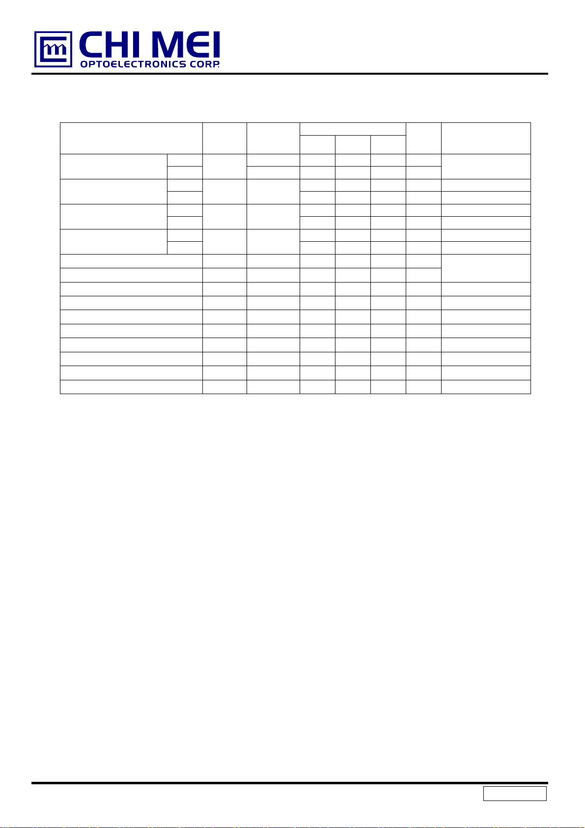
2. ABSOLUTE MAXIMUM RATINGS
2.1 ABSOLUTE RATINGS OF ENVIRONMENT
Item Symbol
Storage Temperature TST -20 +60 ºC (1)
Operating Ambient Temperature TOP 0 50 ºC (1), (2)
Shock (Non-Operating) S
Vibration (Non-Operating) V
Note (1) Temperature and relative humidity range is shown in the figure below.
(a) 90 %RH Max. (Ta ≦ 40 ºC).
(b) Wet-bulb temperature should be 39 ºC Max. (Ta > 40 ºC).
(c) No condensation.
Note (2) The maximum operating temperature is based on the test condition that the surface temperature of
display area is less than or equal to 65 ºC with LCD module alone in a temperature controlled chamber.
Thermal management should be considered in final product design to prevent the surface temperature
- 50 G (3), (5)
NOP
- 1.0 G (4), (5)
NOP
Min. Max.
Value
Unit Note
of display area from being over 65 ºC. The range of operating temperature may degrade in case of
improper thermal management in final product design.
Note (3) 11 ms, half sine wave, 1 time for ± X, ± Y, ± Z.
Note (4) 10 ~ 200 Hz, 10 min, 1 time each X, Y, Z.
Note (5) At testing Vibration and Shock, the fixture in holding the module has to be hard and rigid enough so that
the module would not be twisted or bent by the fixture.
6
Version 2.0

2.2 ELECTRICAL ABSOLUTE RATINGS
2.2.1 TFT LCD MODULE
Issue Date: Dec.21.2006
Model No.:V420H1-L07
Approval
Item Symbol
Min. Max.
Power Supply Voltage VCC -0.3 13.5 V
Logic Input Voltage VIN -0.3 3.6 V
Value
Unit Note
(1)
2.2.2 BACKLIGHT INVERTER UNIT
Item Symbol
Lamp Voltage VW
Power Supply Voltage VBL 0 30 V
Control Signal Level
Note (1) Permanent damage to the device may occur if maximum values are exceeded. Function operation
should be restricted to the conditions described under Normal Operating Conditions.
Note (2) No moisture condensation or freezing.
Note (3)The control signals include On/Off Control, Internal PWM Control, External PWM Control.
-
Value
Min. Max.
-
-0.3 7 V
3000 V
Unit Note
RMS
(1)
(1), (3)
7
Version 2.0
3. ELECTRICAL CHARACTERISTICS
3.1 TFT LCD MODULE (Ta = 25 ± 2 ºC)
Parameter Symbol
Power Supply Voltage VCC 10.8 12 13.2 V (1)
Power Supply Ripple Voltage VRP - - 350 mV
Rush Current I
White 1.35 1.7 A
Power Supply Current
Differential Input High
Differential Input Low
LVDS
Interface
Common Input Voltage
Terminating Resistor
CMOS
interface
Input High Threshold Voltage
Input Low Threshold Voltage
Black 0.5 A
Vertical Stripe
Threshold Voltage V
Threshold Voltage V
Issue Date: Dec.21.2006
Model No.:V420H1-L07
Value
Unit Note
RUSH
Min. Typ. Max.
- - 4.0 A (2)
-
-
-
LVT H
LVT L
V
LVC
R
- 100 - ohm
T
2.7 - 3.3 V
V
IH
V
0 - 0.7 V
IL
1.0 A
- - 100 mV
-100 - - mV
1.125 1.25 1.375 V
Approval
(3)
Note (1) The module should be always operated within the above ranges.
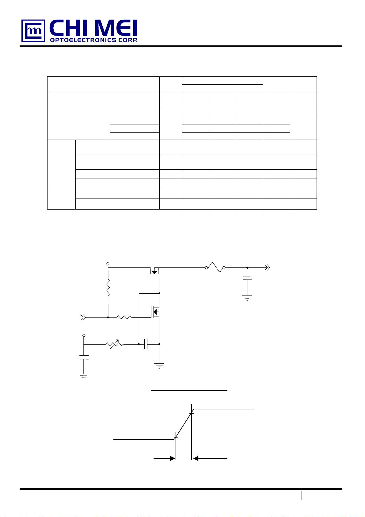
Note (2) Measurement condition:
Vs (12V)
R1
47K
Q1 2SK1475
FUSE
(High to Low)
(Control Signal)
SW
+24V
C1
1uF
VR1
47K
R2
1K
0.01uF
Q2
2SK1470
C2
Vcc rising time is 470us
Vcc
C3
1uF
Vcc
(LCD Module Input)
0.9Vcc
0.1Vcc
GND
470us
8
Version 2.0
Issue Date: Dec.21.2006
Model No.:V420H1-L07
Approval
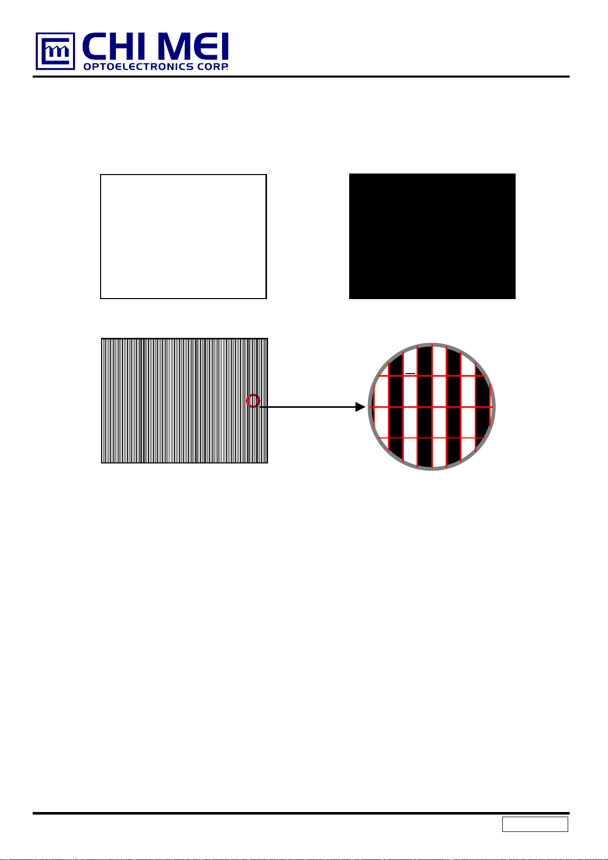
Note (3) The specified power supply current is under the conditions at Vcc = 12 V, Ta = 25 ± 2 ºC, fv = 60 Hz,
whereas a power dissipation check pattern below is displayed.
a. White Pattern
Active Area
c. Vertical Stripe Pattern
b. Black Pattern
Active Area
R
G
R
B
G
R
B
G
R R
G
B
B
B
B
R
R
R
G
G
G
G
B
B
B
B
R
R
Active Area
9
Version 2.0

Issue Date: Dec.21.2006
Model No.:V420H1-L07
Approval
3.2 BACKLIGHT UNIT
3.2.1 CCFL (Cold Cathode Fluorescent Lamp) CHARACTERISTICS (Ta = 2 5 ± 2 º C)
Parameter Symbol
Min. Typ. Max.
Lamp Input Voltage VL - 1520 - V
Lamp Current IL 5.3 5.8 6.3 mA
Lamp Turn On Voltage VS
- -
- Operating Frequency FL 40 - 70 KHz
Lamp Life Time LBL 50,000 60,000 - Hrs (2)
3.2.2 INVERTER CHARACTERISTICS (Ta = 25 ± 2 ºC)
Parameter Symbol
Power Consumption at
Gray level 255
Power Consumption at
Gray level 128
Power Consumption at
Gray level 0
P
- 170 180 W (5)(6), IL =5.8mA
255
P
- 85 - W
128
P
- 60 - W
0
Power Supply Voltage VBL 22.8 24 25.2 VDC
Power Supply Current IBL - 7.1 - A Non Dimming
Input Ripple Noise - - - 912 mV
Backlight Turn on
Voltage
V
BS
Oscillating Frequency FW 47 50 53 kHz
Dimming frequency FB 150 160 170 Hz
Minimum Duty Ratio D
- 20 - %
MIN
Note (1) Lamp current is measured by utilizing AC current probe and its value is average by measuring
Min. Typ. Max.
2370
2160 - - V
Value
Unit Note
V
V
Value
2370
2160
- -
-
RMS
(1)
RMS
Ta = 0 º C
RMS
Ta = 25 ºC
RMS
Unit Note
VBL=22.8V
P-P
V
Ta = 0 ºC
RMS
Ta = 25 ºC
RMS
master and slave board.
Note (2) The lamp starting voltage V
should be applied to the lamp for more than 1 second after startup.
S
Otherwise the lamp may not be turned on.
Note (3) The lamp frequency may produce interference with horizontal synchronous frequency of the
display input signals, and it may result in line flow on the display. In order to avoid interference, the
lamp frequency should be detached from the horizontal synchronous frequency and its harmonics
as far as possible.
Note (4) The life time of a lamp is defined as when the brightness is larger than 50% of its original value and
the effective discharge length is longer than 80% of its original length (Effective discharge length is
defined as an area that has equal to or more than 70% brightness compared to the brightness at
the center point of lamp.) as the time in which it continues to operate under the condition at Ta = 25
±2℃ and I
Note (5) The power supply capacity should be higher than the total inverter power consumption P
= 5.3~ 6.3mArms.
L
. Since
BL
the pulse width modulation (PWM) mode was applied for backlight dimming, the driving current
changed as PWM duty on and off. The transient response of power supply should be considered
for the changing loading when inverter dimming.
10
Version 2.0
Issue Date: Dec.21.2006
Model No.:V420H1-L07
Approval
Note (6) The measurement condition of Max. value is based on 42" backlight unit under input voltage 24V,
average lamp current 6.1 mA and lighting 30 minutes later.
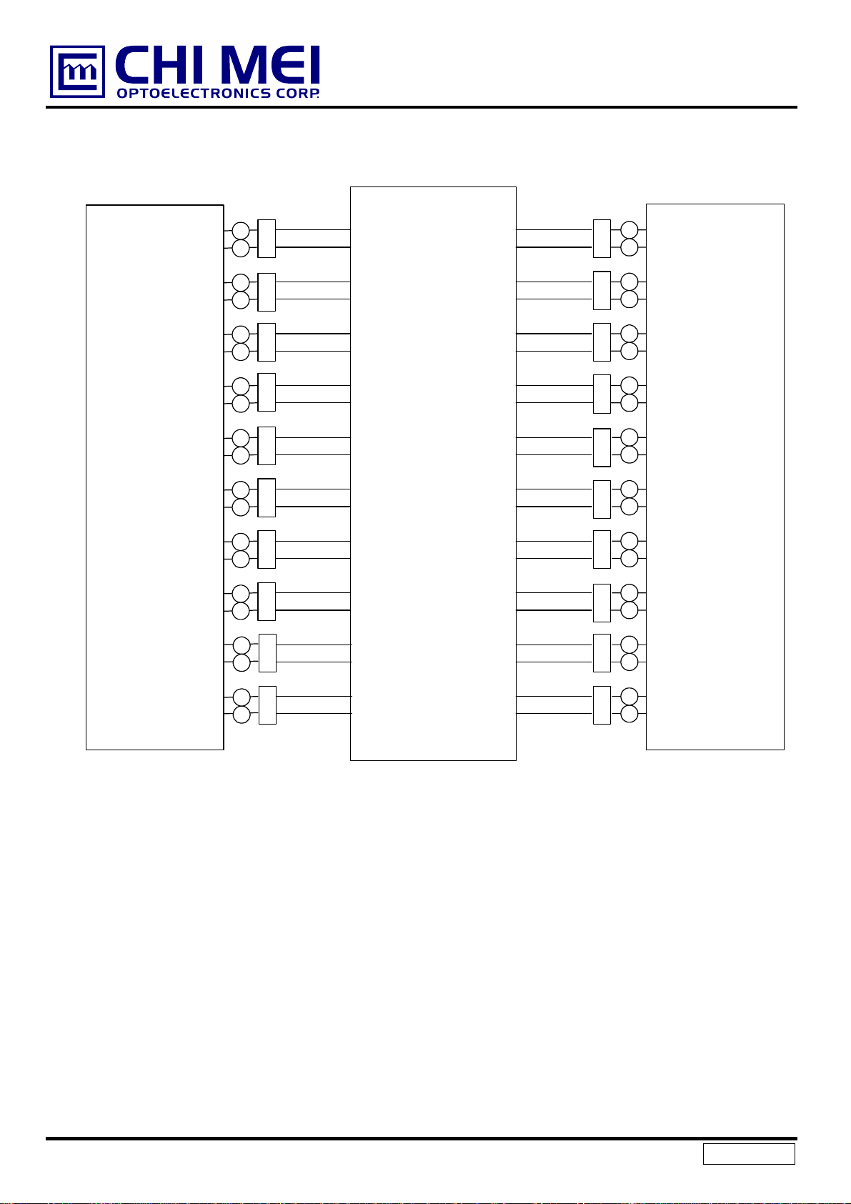
Inverter
(Master)
A
A
A
A
A
A
A
A
A
A
A
A
A
A
A
A
HV (White -)
1
HV(Pink -)
2
HV (White +)
1
HV(Pink +)
2
HV (White -)
1
HV(Pink -)
2
HV (White +)
1
HV(Pink +)
2
HV (White -)
1
HV(Pink -)
2
HV (White +)
1
HV(Pink +)
2
HV (White -)
1
HV(Pink -)
2
HV (White +)
1
HV(Pink +)
2
LCD Module
HV (Pink +)
HV (White +)
HV (Pink -)
HV (White -)
HV (Pink +)
HV (White +)
HV (Pink -)
HV (White -)
HV (Pink +)
HV (White +)
HV (Pink -)
HV (White -)
HV (Pink +)
HV (White +)
HV (Pink -)
HV (White -)
A
1
2
A
A
1
2
A
A
1
2
A
A
1
2
A
A
1
2
A
A
1
2
A
A
1
2
A
A
1
2
A
Inverter
(Slavor)
A
A
A
A
HV(Blue -)
1
HV (Pink -)
2
HV(Blue +)
1
HV (Pink +)
2
HV (Pink +)
HV (White +)
HV (Pink -)
HV (White -)
A
1
2
A
A
1
2
A
11
Version 2.0
Issue Date: Dec.21.2006
y
y
Model No.:V420H1-L07
Approval
3.2.3 INVERTER INT ERFACE CHAR ACTERISTICS
2.0
0
-
0
0
1
Value
-
-
0
-
-
-
5.0 V
0.8 V
-
5.0 V duty on External PWM Control
0.8 V dut
0.8 V abnormal
100 ms
100 ms
50 us
50 us
- - MΩ
Unit Note
V minimum dut
ratio
off
See as below
Parameter Symbol
On/Off Control Voltage
Voltage
Voltage
Status Signal
ON
OFF
MAX 2.85 3.0 3.15 V maximum duty ratioInternal PWM Control
MIN
HI 2.0
LO
HI 3.0 3.3 3.6 V normal
LO
V
BLON
V
IPWM
V
EPWM
Status
Condition
Tes t
Min. Typ. Max.
-
-
-
-
-
VBL Rising Time Tr1 - 30 - 50 ms
VBL Falling Time Tf1 - 30 - 50 ms
Control Signal Rising Time Tr
Control Signal Falling Time Tf
PWM Signal Rising Time T
PWM Signal Falling Time T
PWMR
PWMF
Input impedance RIN
PWM Delay Time T
BLON Delay Time T
BLON Off Time T
PWM
on
off
- 100 300 mS
- 1 - - ms
- 1 - - ms
- - -
- - -
- - -
- - -
-
Note (1) The Dimming signal should be valid before backlight turns on by BLON signal. It is inhibited to
change the internal/external PWM signal during backlight turn on period.
Note (2) The power sequence and control signal timing are shown in the following figure.
Note (3) The power sequence and control signal timing must follow the figure below. For a certain reason,
the inverter has a possibility to be damaged with wrong power sequence and control signal
timing.
12
Version 2.0
 Loading...