

Chimei V400H1-L01 Schematic
Issued Date: Aug. 02, 2007
1
Model No.: V400H1 - L01
TFT LCD Approval Specification
MODEL NO.: V400H1 - L01
Customer:
Approval
Approved by:
Note:
TVHD
Approved By
LY Chen
Reviewed By
QRA Dept. Product Development Div.
Tomy Chen WT Lin
LCD TV Marketing and Product Management Div.
Prepared By
Denise Shieh Gina Tsou
Version 2.0

Issued Date: Aug. 02, 2007
2
Model No.: V400H1 - L01
- CONTENTS -
REVISION HISTORY
1. GENERAL DESCRIPTION
1.1 OVERVIEW
1.2 FEATURES
1.3 APPLICATION
1.4 GENERAL SPECIFICATIONS
1.5 MECHANICAL SPECIFICATIONS
2. ABSOLUTE MAXIMUM RATINGS
2.1 ABSOLUTE RATINGS OF ENVIRONMENT
2.2 PACKAGE STORAGE
2.3 ELECTRICAL ABSOLUTE RATINGS
2.3.1 TFT LCD MODULE
2.3.2 BACKLIGHT UNIT
3. ELECTRICAL CHARACTERISTICS
3.1 TFT LCD MODULE
3.2 BACKLIGHT UNIT
3.2.1 CCFL(Cold Cathode Fluorescent Lamp) CHARACTERISTICS
3.2.2 BALANCE BOARD CHARACTERISTICS
4. BLOCK DIAGRAM
4.1 TFT LCD MODULE
5. INTERFACE PIN CONNECTION
5.1 TFT LCD MODULE
5.2 BACKLIGHT UNIT
5.3 BALANCE BOARD UNIT
5.4 BLOCK DIAGRAM OF INTERFACE
5.5 LVDS INTERFACE
5.6 COLOR DATA INPUT ASSIGNMENT
6. INTERFACE TIMING
6.1 INPUT SIGNAL TIMING SPECIFICATIONS
6.2 POWER ON/OFF SEQUENCE
7. OPTICAL CHARACTERISTICS
7.1 TEST CONDITIONS
7.2 OPTICAL SPECIFICATIONS
8. DEFINITION OF LABELS
8.1 CMO MODULE LABEL
9. PACKAGING
9.1 PACKING SPECIFICATIONS
9.2 PACKING METHOD
10. PRECAUTIONS
10.1 ASSEMBLY AND HANDLING PRECAUTIONS
10.2 SAFETY PRECAUTIONS
10.3 SAFETY STANDARDS
11. MECHANICAL CHARACTERISTICS
-------------------------------------------------------
-------------------------------------------------------
-------------------------------------------------------
-------------------------------------------------------
-------------------------------------------------------
-------------------------------------------------------
-------------------------------------------------------
-------------------------------------------------------
-------------------------------------------------------
-------------------------------------------------------
-------------------------------------------------------
-------------------------------------------------------
Approval
3
4
5
7
11
12
21
24
28
29
31
32
Version 2.0
Issued Date: Aug. 02, 2007
3
Model No.: V400H1 - L01
Version
Ver 2.0
REVISION HISTORY
Date
Aug. 02,’07 All All Approval Specification was first issued.
Page
(New)
Section
Description
Approval
Version 2.0

Issued Date: Aug. 02, 2007
4
Model No.: V400H1 - L01
1. GENERAL DESCRIPTION
1.1 OVERVIEW
V400H1- L01 is a 40” TFT Liquid Crystal Display module with 20-CCFL Backlight unit and 2ch-LVDS
interface. This module supports 1920 x 1080 FHD format and can display true 16.7M colors (8-bit colors).
The inverter module for backlight is built-in.
1.2 FEATURES
- High brightness (550 nits)
- Ultra-high contrast ratio (1800:1)
- Faster response time (Gray to gray average 6.5ms)
- High color saturation NTSC 72%
- Ultra wide viewing angle : 176(H)/176(V) (CR>20) with Super MVA technology
- DE (Data Enable) only mode
- LVDS (Low Voltage Differential Signaling) interface
- Color reproduction (nature color)
Approval
- Optimized response time for both 50/60 Hz Frame rate
- Low color shift function
- RoHS compliance
1.3 APPLICATION
- TFT LCD TVs
- Multi-Media Display
1.4 GENERAL SPECIFICATI0NS
Item Specification Unit Note
Active Area 885.6(H) x 498.15 (V) (40” diagonal) mm
Bezel Opening Area 891.7 (H) x 504.2 (V) mm
Driver Element a-si TFT active matrix -
Pixel Number 1920 x R.G.B. x 1080 pixel
Pixel Pitch (Sub Pixel) 0.1730 (H) x 0.5190 (V) mm
Pixel Arrangement RGB vertical stripe -
Display Colors 16.7M color
Display Operation Mode Transmissive mode / Normally black -
Surface Treatment Anti-Glare coating (Haze 25%),Hard coating (3H)
(1)
-
1.5 MECHANICAL SPECIFICATIONS
Item Min. Typ. Max. Unit Note
Horizontal(H) 951 952 953 mm (1)
Module Size
Note (1) Please refer to the attached drawings for more information of front and back outline dimensions.
Vertical(V) 550 551 552 mm (1)
Depth(D) 45.6 46.6 47.6 mm To PCB cover
Depth(D) 52.2 53.2 54.2 mm To inverter cover
Weight - 10350 - g
Version 2.0
Issued Date: Aug. 02, 2007
5
80 60
80 40 60 20 10
Model No.: V400H1 - L01
2. ABSOLUTE MAXIMUM RATINGS
2.1 ABSOLUTE RATINGS OF ENVIRONMENT
Item Symbol
Storage Temperature TST -20 +60 ºC (1)
Operating Ambient Temperature TOP 0 +50 ºC (1), (2)
Shock (Non-Operating) S
Vibration (Non-Operating) V
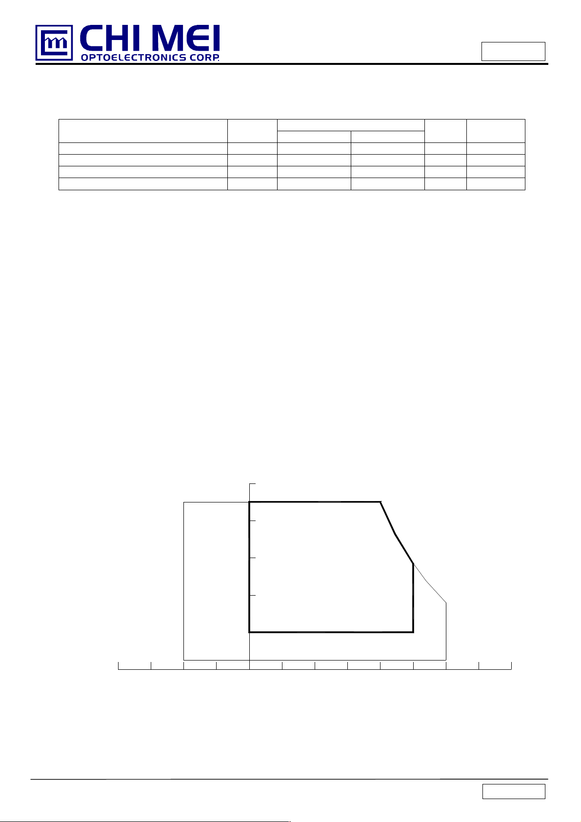
Note (1) Temperature and relative humidity range is shown in the figure below.
(a) 90 %RH Max. (Ta 40 ºC).
(b) Wet-bulb temperature should be 39 ºC Max. (Ta > 40 ºC).
(c) No condensation.
Note (2) The maximum operating temperature is based on the test condition that the surface temperature of
display area is less than or equal to 60 ºC with LCD module alone in a temperature controlled chamber.
Thermal management should be considered in final product design to prevent the surface temperature of
display area from being over 60 ºC. The range of operating temperature may degrade in case of improper
- 50 G (3), (5)
NOP
- 1.0 G (4), (5)
NOP
Min. Max.
Value
Unit Note
Approval
thermal management in final product design.
Note (3) 11 ms, half sine wave, 1 time for ± X, ± Y, ± Z.
Note (4) 10 ~ 200 Hz, 10 min, 1 time each X, Y, Z.
Note (5) At testing Vibration and Shock, the fixture in holding the module has to be hard and rigid enough
so that the module would not be twisted or bent by the fixture.
Relative Humidity (%RH)
100
90
Operating Range
-40
-20 40
Storage Range
0 20
Temperature (ºC)
Version 2.0
Issued Date: Aug. 02, 2007
6
Value
Min. M
ax.
Lamp Voltage
V
3000
V
Model No.: V400H1 - L01
2.2 PACKAGE STORAGE
When storing modules as spares for a long time, the following precaution is necessary.
(a) Do not leave the module in high temperature, and high humidity for a long time. It is highly recommended to
store the module with temperature from 0 to 35at normal humidity without condensation.
(b) The module shall be stored in dark place. Do not store the TFT-LCD module in direct sunlight or fluorescent
light.
2.3 ELECTRICAL ABSOLUTE RATINGS
2.3.1 TFT LCD MODULE
Item Symbol
Power Supply Voltage Vcc -0.3 13.5 V
Input Signal Voltage VIN -0.3 3.6 V
Min. Max.
Value
Unit Note
(1)
2.3.2 BACKLIGHT UNIT
Approval
Item Symbol
Note (1) No moisture condensation or freezing.
Unit Note
Version 2.0
Issued Date: Aug. 02, 2007
7
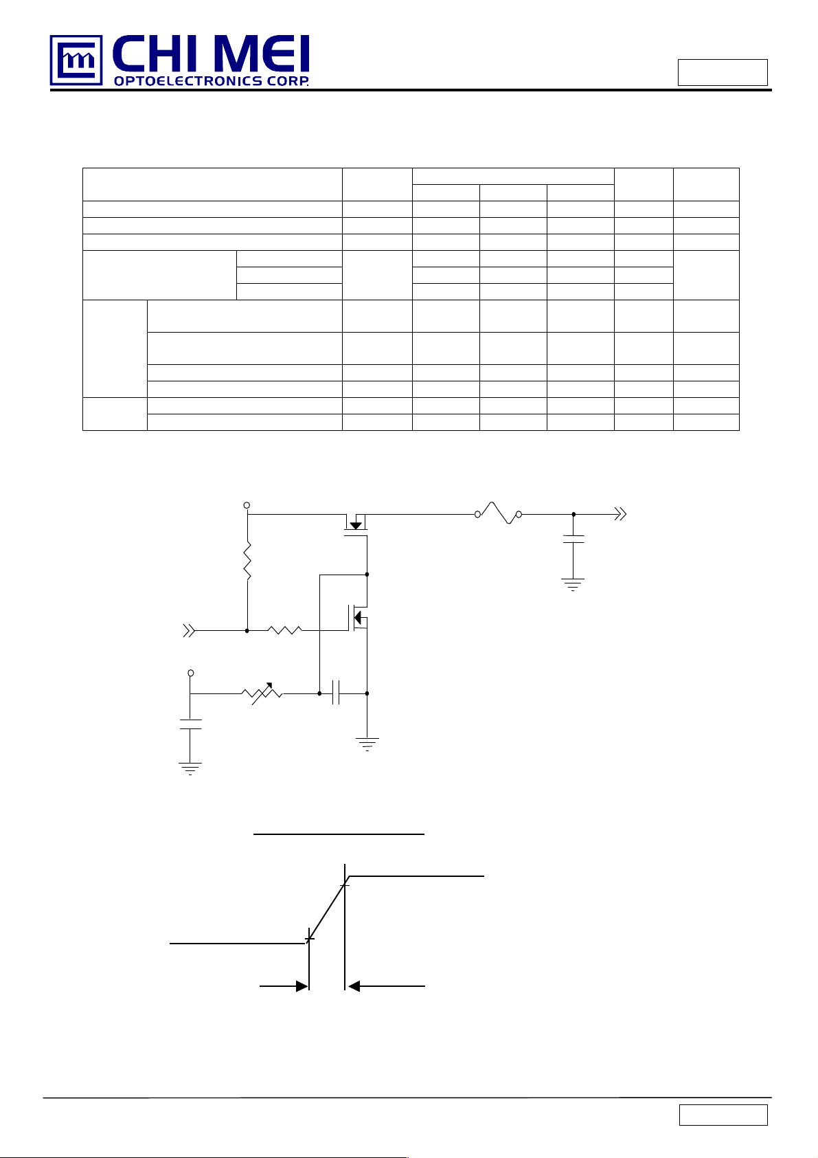
(High to Low)
SW Q2 C1
Q1
R2 1K
C2
C3
Model No.: V400H1 - L01
3. ELECTRICAL CHARACTERISTICS
3.1 TFT LCD MODULE
Parameter Symbol
Power Supply Voltage VCC 10.8 12.0 13.2 V (1)
Power Supply Ripple Voltage VRP - - 350 mV
Rush Current I
White - 1.2 1.5 A
Power Supply Current
Differential Input High
LVDS
Interface
Threshold Voltage
Differential Input Low
Threshold Voltage
Common Input Voltage V
Terminating Resistor R
Input High Threshold Voltage VIH 2.7 - 3.3 V CMOS
interface
Input Low Threshold Voltage VIL 0 - 0.7 V
Note (1) The module should be always operated within above ranges.
Note (2) Measurement Conditions:
Black - 0.6 0.7 A
Vertical Stripe
+12.0V
R1
47K
Ta = 25 ± 2 ºC
Value
Min. Typ. Max.
- - 4.5 A (2)
RUSH
Unit Note
ICC
- 1.0 1.2 A
V
- - +100 mV
LVTH
-100 - - mV
V
LVTL
1.125 1.25 1.375 V
LVC
- 100 - ohm
T
2SK1475
Vcc
FUSE
1uF
(LCD Module Input)
Approval
(3)
(Control Signal)
+15V
VR1
2SK1470
47K
1uF
0.01uF
Vcc rising time is 470us
+12V
0.9Vcc
0.1Vcc
GND
470us
Version 2.0
Issued Date: Aug. 02, 2007
8
- 1400
-
RMS
7.7 8.0 8.3
RMS
RMS
(2)
, Ta = 0
ºC
RMS
(2)
, Ta = 25
ºC
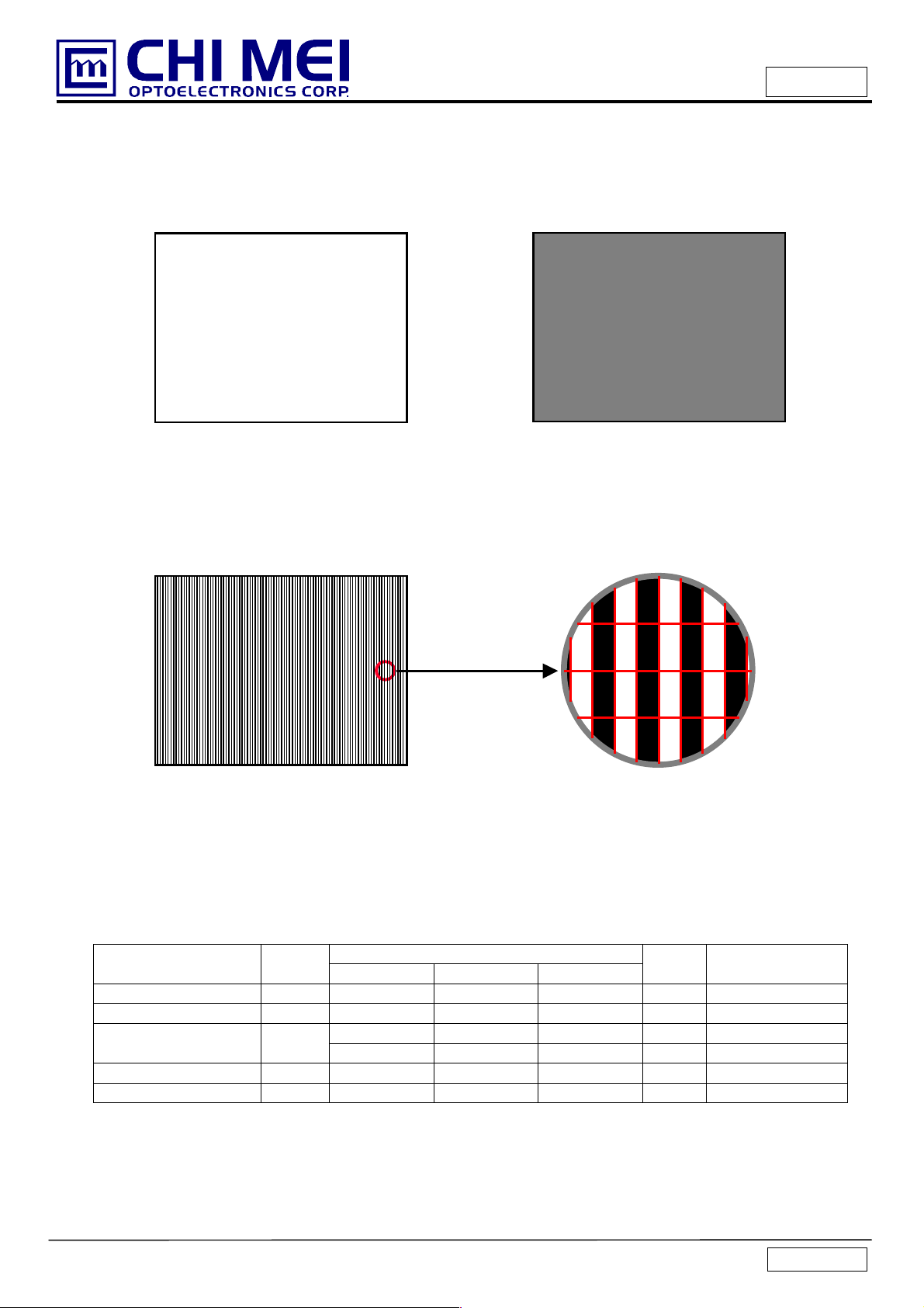
R R R R R R R G G G G B B B B B B G G G G B B B B R R
Model No.: V400H1 - L01
Note (3) The specified power supply current is under the conditions at Vcc = 12 V, Ta = 25 ± 2 ºC, fv = 60
Hz, whereas a power dissipation check pattern below is displayed.
a. White Pattern
Active Area
b. Black Pattern
Active Area
Approval
c. Vertical Stripe Pattern
Active Area
3.2 BACKLIGHT UNIT
3.2.1 CCFL (Cold Cathode Fluorescent Lamp) CHARACTERISTICS (
Parameter Symbol
Lamp Voltage VW
Lamp Current IL
Lamp Starting Voltage
Operating Frequency FO 40 - 70
Lamp Life Time LBL 50,000 - -
VS
Min. Typ. Max.
- -
- -
Value
R
2290
2060
Ta = 25 ± 2 ºC)
Unit Note
V
Ih = 8.0mA
mA
V
V
KHz (3)
Hrs (4)
(1)
Version 2.0
Issued Date: Aug. 02, 2007
9
BL
(HV)
Oscillating Frequency
MIN
Model No.: V400H1 - L01
3.2.2 BALANCE BOARD CHARACTERISTICS (
Parameter Symbol
Input High Voltage V
Input Current I
(HV1/HV2
Min. Typ. Max.
- 1400 - V (2)
175 mArms
Ta = 25 ± 2 ºC)
Value
Unit Note
FW 41 44 47 kHz
Individual Lamp Current
High (LD) LD
I
7.7 8.0 8.3 mA H.V
L
5
V Normal Operation
Lamp Detection
Low (LD) LD
1.5
V Lamp Connector Open
Dimming frequency FB 150 160 170 Hz
Minimum Duty Ratio D
- 15 - %
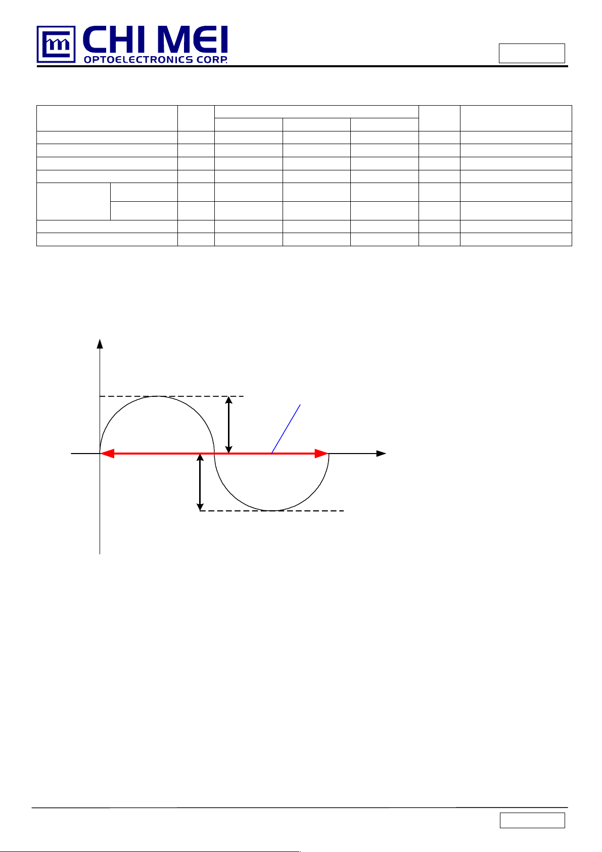
Note (1) Lamp current is measured by utilizing high frequency current meters as shown below:
Note (2) Input High Voltage Hv based on spec. +-7% tolerance.
Note (3) Asymmetric ratio must be from 90% to 110% (0.9<Ip/ I
rms@T/2X2
<1.1)
Approval
No Dimming
T
Ip
I-p
Version 2.0
Issued Date: Aug. 02, 2007
10
Model No.: V400H1 - L01
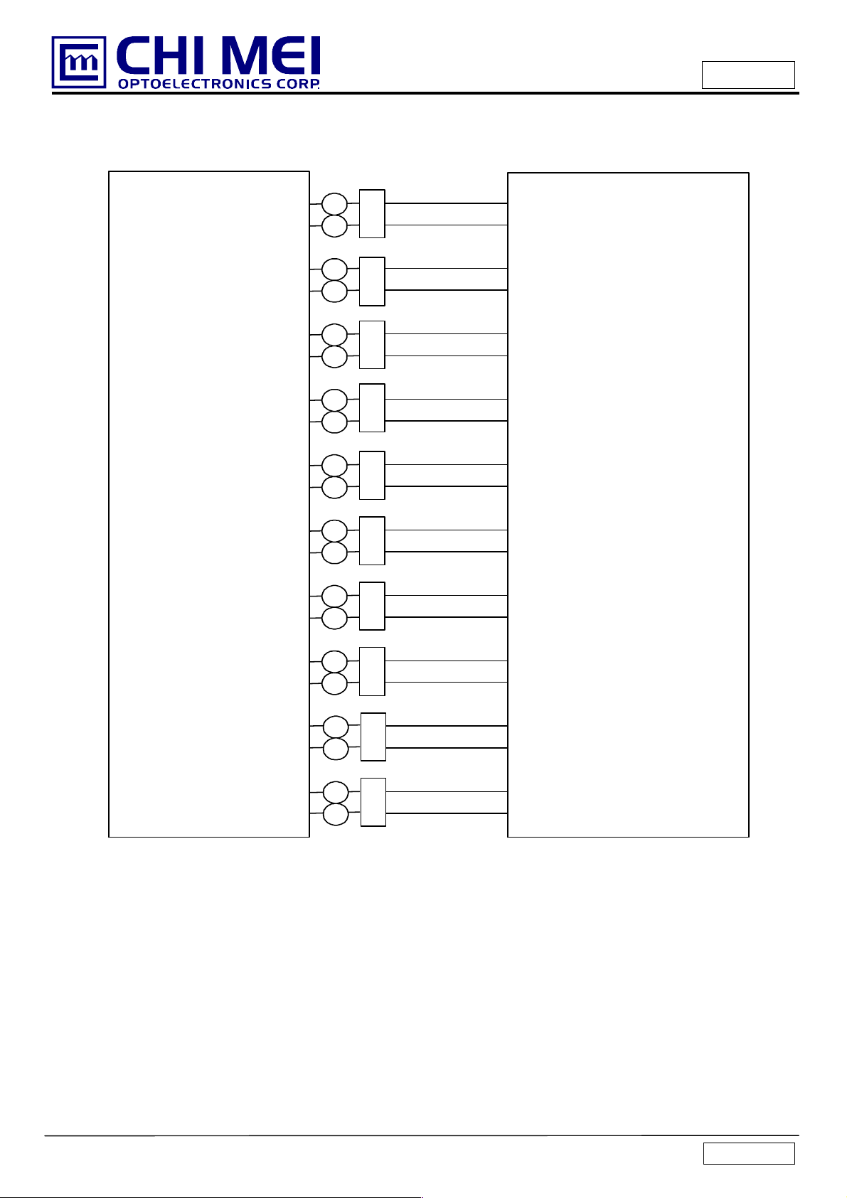
Approval
HV (Blue +)
1
Balance
Board
A
A
A
A
A
A
A
A
A
A
HV (White -)
2
HV (Blue +)
1
HV (White -)
2
HV (Blue +)
1
HV (White -)
2
HV (Blue +)
1
HV (White -)
2
HV (Blue +)
1
HV (White -)
2
LCD M odule
A
A
A
A
A
A
A
A
A
A
HV (Blue +)
1
HV (White -)
2
HV (Blue +)
1
HV (White -)
2
HV (Blue +)
1
HV(W hite -)
2
HV (Blue +)
1
HV (White -)
2
HV (Blue +)
1
HV (White -)
2
Version 2.0
 Loading...