

chimei N156BGE-E31 Datasheet
PRODUCT SPECIFICATION
Customer:
Doc. Number:
□ Tentative Specification
▓ Preliminary Specification
□ Approval Specification
MODEL NO.: N156BGE
SUFFIX: E31
APPROVED BY SIGNATURE
Name / Title
Note
Please return 1 copy for your confirmation with your
signature and comments.
Approved By Checked By Prepared By
楊竣傑
楊竣傑
楊竣傑楊竣傑
2013-03-29
18:33:22 CST
曹文彬
曹文彬
曹文彬曹文彬
2013-03-27
16:56:13 CST
孫莉
孫莉
孫莉孫莉
2013-03-04
18:20:09 CST
Version 1.1 1 March 2013 1 / 37
The copyright belongs to InnoLux. Any unauthorized use is prohibited.

PRODUCT SPECIFICATION
CONTENTS
1. GENERAL DESCRIPTION.........................................................................................................4
1.1 OVERVIEW ................................................................................................................................4
1.2 GENERAL SPECIFICATI0NS ...................................................................................................4
2. MECHANICAL SPECIFICATIONS .............................................................................................5
2.1 CONNECTOR TYPE..................................................................................................................5
3. ABSOLUTE MAXIMUM RATINGS .............................................................................................6
3.1 ABSOLUTE RATINGS OF ENVIRONMENT ..........................................................................6
3.2 ELECTRICAL ABSOLUTE RATINGS......................................................................................6
3.2.1 TFT LCD MODULE............................................................................................................6
4. ELECTRICAL SPECIFICATIONS...............................................................................................7
4.1 FUNCTION BLOCK DIAGRAM...............................................................................................7
4.2. INTERFACE CONNECTIONS .................................................................................................7
4.3 ELECTRICAL CHARACTERISTICS........................................................................................9
4.3.1 LCD ELETRONICS SPECIFICATION...............................................................................9
4.3.2 LED CONVERTER SPECIFICATION..............................................................................11
4.3.3 BACKLIGHT UNIT...........................................................................................................13
4.4 INPUT SIGNAL TIMING SPECIFICATIONS ........................................................................14
4.4.1 DISPLAY PORT INTERFACE ..........................................................................................14
4.4.2 COLOR DATA INPUT ASSIGNMENT ............................................................................15
4.5 DISPLAY TIMING SPECIFICATIONS ...................................................................................16
4.6 POWER ON/OFF SEQUENCE ................................................................................................17
5. OPTICAL CHARACTERISTICS ...............................................................................................19
5.1 TEST CONDITIONS.................................................................................................................19
5.2 OPTICAL SPECIFICATIONS ..................................................................................................19
6. RELIABILITY TEST ITEM ........................................................................................................22
7. PACKING..................................................................................................................................23
7.1 MODULE LABEL ....................................................................................................................23
7.2 CARTON ...................................................................................................................................24
7.3 PALLET.....................................................................................................................................24
7.3 PALLET.....................................................................................................................................25
8. PRECAUTIONS........................................................................................................................26
8.1 HANDLING PRECAUTIONS..................................................................................................26
8.2 STORAGE PRECAUTIONS ....................................................................................................26
8.3 OPERATION PRECAUTIONS.................................................................................................26
Appendix. EDID DATA STRUCTURE...........................................................................................27
Appendix. OUTLINE DRAWING..................................................................................................30
Appendix. SYSTEM COVER DESIGN GUIDANCE....................................................................32
Version 1.1 1 March 2013 2 / 37
The copyright belongs to InnoLux. Any unauthorized use is prohibited.
PRODUCT SPECIFICATION
REVISION HISTORY
Version
1.0 Dec. 08, 2012 All Preliminary Specification Ver.1.0 was first issued.
1.1 Mar. 01, 2013
31 Modify “Appendix.
Date Page Description
All Change logo & content from “CHIMEI INNOLUX” to “INNOLUX”
SYSTEM COVER DESIGN GUIDANCE”
Version 1.1 1 March 2013 3 / 37
The copyright belongs to InnoLux. Any unauthorized use is prohibited.
PRODUCT SPECIFICATION
1. GENERAL DESCRIPTION
1.1 OVERVIEW
N156BGE-E31 is a 15.6” (1
unit and 30 pins eDP interface. This module supports 1366 x 768 HD mode and can display
262,144 colors. The optimum viewing angle is at 6 o’clock direction.
5.6
” diagonal) TFT Liquid Crystal Display module with LED Backlight
1.2 GENERAL SPECIFICATI0NS
Item Specification Unit Note
Screen Size 15.6” diagonal
Driver Element a-si TFT active matrix - Pixel Number 1366 x R.G.B. x 768 pixel Pixel Pitch 0.252 (H) x 0.252 (V) mm Pixel Arrangement RGB vertical stripe - Display Colors 262,144 color Transmissive Mode Normally white - Surface Treatment Hard coating (3H), Anti-Glare - Luminance, White 200 Cd/m2
Power Consumption Total (2.86) W (Max.) @ cell (1.0) W (Max.), BL (1.86) W (Max.) (1)
Note (1) The specified power consumption (with converter efficiency) is under the conditions at VCCS =
3.3 V, fv = 60 Hz, LED_VCCS = Typ, fPWM = 200 Hz, Duty=100% and Ta = 25 ± 2 ºC, whereas Mosaic
pattern is displayed.
Version 1.1 1 March 2013 4 / 37
The copyright belongs to InnoLux. Any unauthorized use is prohibited.
PRODUCT SPECIFICATION
Pin1 Pin30
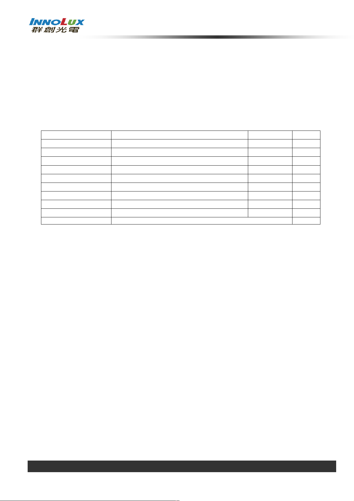
2. MECHANICAL SPECIFICATIONS
Item Min. Typ. Max. Unit Note
Horizontal (H) 359 359.5 360 mm
Vertical (V) w/o
Module Size
Bezel Area
Active Area
Note (1) Please refer to the attached drawings for more information of front and back outline dimensions.
PCB and Hinge
Vertical (V) with
PCB w/o Hinge
Thickness (T) - 3.5 3.8 mm
Horizontal 347.06 347.36 347.66 mm
Vertical 196.29 196.59 196.89 mm
Horizontal 343.932 344.232 344.532 mm
Vertical 193.236 193.536 193.836 mm
Weight - 410 425 g
2.1 CONNECTOR TYPE
206 206.5 207 mm
217 217.5 218 mm
(1)
Please refer Appendix Outline Drawing for detail design.
Connector Part No.: IPEX-20455-030E-12
User’s connector Part No: IPEX-20453-030T-01
Version 1.1 1 March 2013 5 / 37
The copyright belongs to InnoLux. Any unauthorized use is prohibited.
PRODUCT SPECIFICATION
3. ABSOLUTE MAXIMUM RATINGS
3.1 ABSOLUTE RATINGS OF ENVIRONMENT
Item Symbol
Min. Max.
Storage Temperature TST -20 +60 ºC (1)
Operating Ambient Temperature TOP 0 +50 ºC (1), (2)
Note (1) (a) 90 %RH Max. (Ta <= 40 ºC).
(b) Wet-bulb temperature should be 39 ºC Max. (Ta > 40 ºC).
(c) No condensation.
Note (2) The temperature of panel surface should be 0 ºC min. and 60 ºC max.
Relative Humidity (%RH)
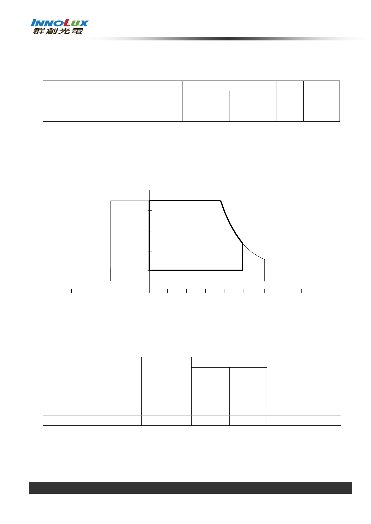
100
90
80
Value
Unit Note
60
Operating Range
40
20
10
Storage Range
Temperature (ºC)
3.2 ELECTRICAL ABSOLUTE RATINGS
3.2.1 TFT LCD MODULE
Item Symbol
Power Supply Voltage VCCS -0.3 +4.0 V
Logic Input Voltage VIN -0.3 VCCS+0.3
Converter Input Voltage
Converter Control Signal Voltage
Converter Control Signal Voltage
LED_VCCS
LED_PWM,
LED_EN
Value
Min. Max.
-0.3 (26) V (1)
-0.3 (5) V (1)
-0.3 (5) V (1)
80 60 -20 40 0 20 -40
Unit Note
(1)
V
Note (1) Stresses beyond those listed in above “ELECTRICAL ABSOLUTE RATINGS” may cause
permanent damage to the device. Normal operation should be restricted to the conditions
described in “ELECTRICAL CHARACTERISTICS”.
Version 1.1 1 March 2013 6 / 37
The copyright belongs to InnoLux. Any unauthorized use is prohibited.
PRODUCT SPECIFICATION
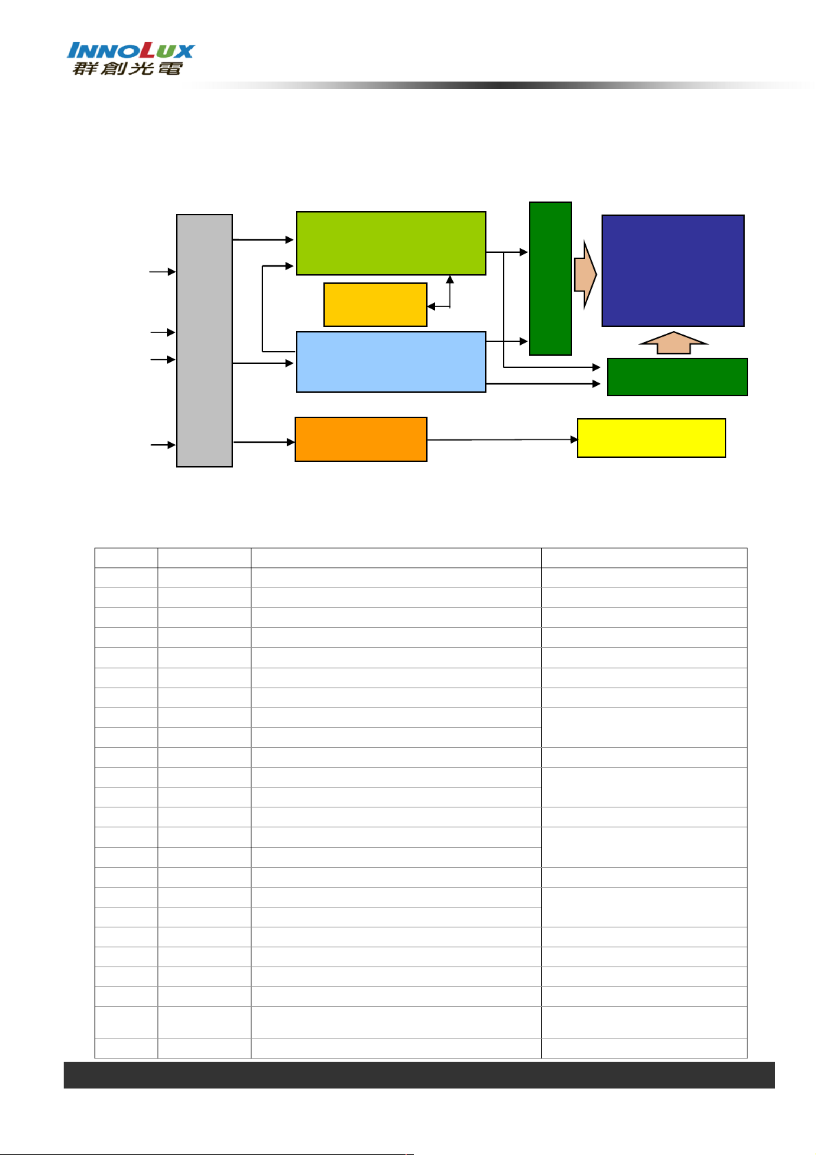
SCAN DRIVER
CIRCUIT
EDID
DC/DC CONVERTER &
LED
4. ELECTRICAL SPECIFICATIONS
4.1 FUNCTION BLOCK DIAGRAM
Display port
Signals
INPUT CONNECTOR
TIMING
CONTROLLER
TFT LCD PANEL
Converter
Input Signals
VCCS
GND
EEPROM
REFERENCE VOLTAGE
GENERATOR
CONVERTER
DATA DRIVER IC
BACKLIGHT UNIT
4.2. INTERFACE CONNECTIONS
PIN ASSIGNMENT
Pin Symbol Description Remark
1 NC No Connection (Reserved)
2 H_GND High Speed Ground
3 NC No Connection (Reserved)
4 NC No Connection (Reserved)
5 H_GND High Speed Ground
6 ML0- Complement Signal-Lane 0
7 ML0+ True Signal-Main Lane 0
8 H_GND High Speed Ground
9 AUX+ True Signal-Auxiliary Channel
10 AUX- Complement Signal-Auxiliary Channel
11 H_GND High Speed Ground
12 VCCS Power Supply +3.3 V (typical)
13 VCCS Power Supply +3.3 V (typical)
14 NC No Connection (Reserved for INNOLUX test)
15 GND Ground
16 GND Ground
17 HPD Hot Plug Detect
18 BL_GND BL Ground
19 BL_GND BL Ground
20 BL_GND BL Ground
21 BL_GND BL Ground
22 LED_EN BL_Enable Signal of LED Converter
23 LED_PWM
24 NC No Connection
PWM Dimming Control Signal of LED
Converter
Version 1.1 1 March 2013 7 / 37
The copyright belongs to InnoLux. Any unauthorized use is prohibited.
PRODUCT SPECIFICATION
Pitch
25 NC No Connection
26 LED_VCCS BL Power
27 LED_VCCS BL Power
28 LED_VCCS BL Power
29 LED_VCCS BL Power
30 NC No Connection (Reserved)
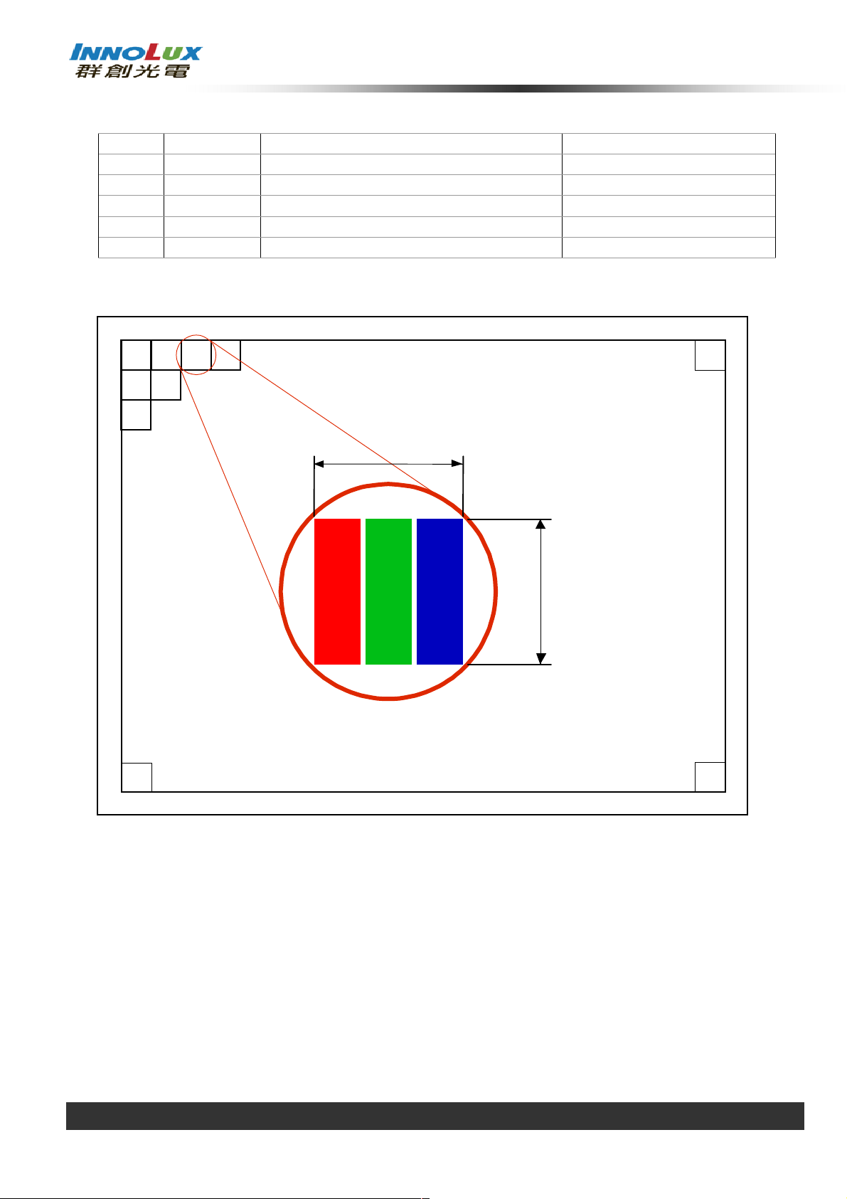
Note (1) The first pixel is odd as shown in the following figure.
1,1
(odd)
2,1
3,1
1,2
(even)
2,2
1,3
(odd)
1,4
(even)
1,Xmax
Pitch
Ymax,
Ymax,1
Xmax
Version 1.1 1 March 2013 8 / 37
The copyright belongs to InnoLux. Any unauthorized use is prohibited.
PRODUCT SPECIFICATION
C2
4.3 ELECTRICAL CHARACTERISTICS
4.3.1 LCD ELETRONICS SPECIFICATION
Parameter Symbol
Min. Typ. Max.
Power Supply Voltage VCCS 3.0 3.3 3.6 V (1)-
Value
Unit Note
HPD
High Level (2.25) - (2.75) V
Low Level (0) - (0.4) V
Ripple Voltage VRP - (50) - mV (1)Inrush Current I
- - (1.5) A (1),(2)
RUSH
Mosaic - (250) (300) mA (3)a
Power Supply Current
Black
lcc
- (300) (340) mA (3)
Note (1) The ambient temperature is Ta = 25 ± 2 ºC.
Note (2) I
: the maximum current when VCCS is rising
RUSH
IIS: the maximum current of the first 100ms after power-on
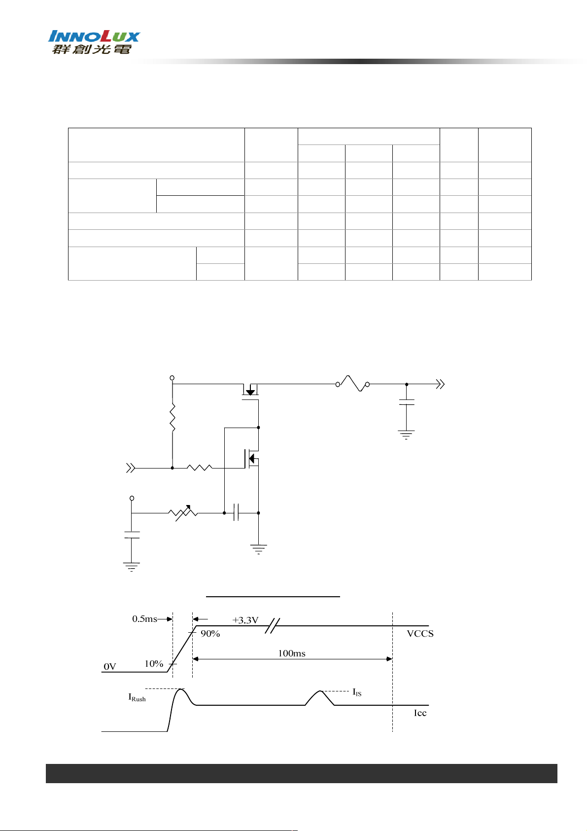
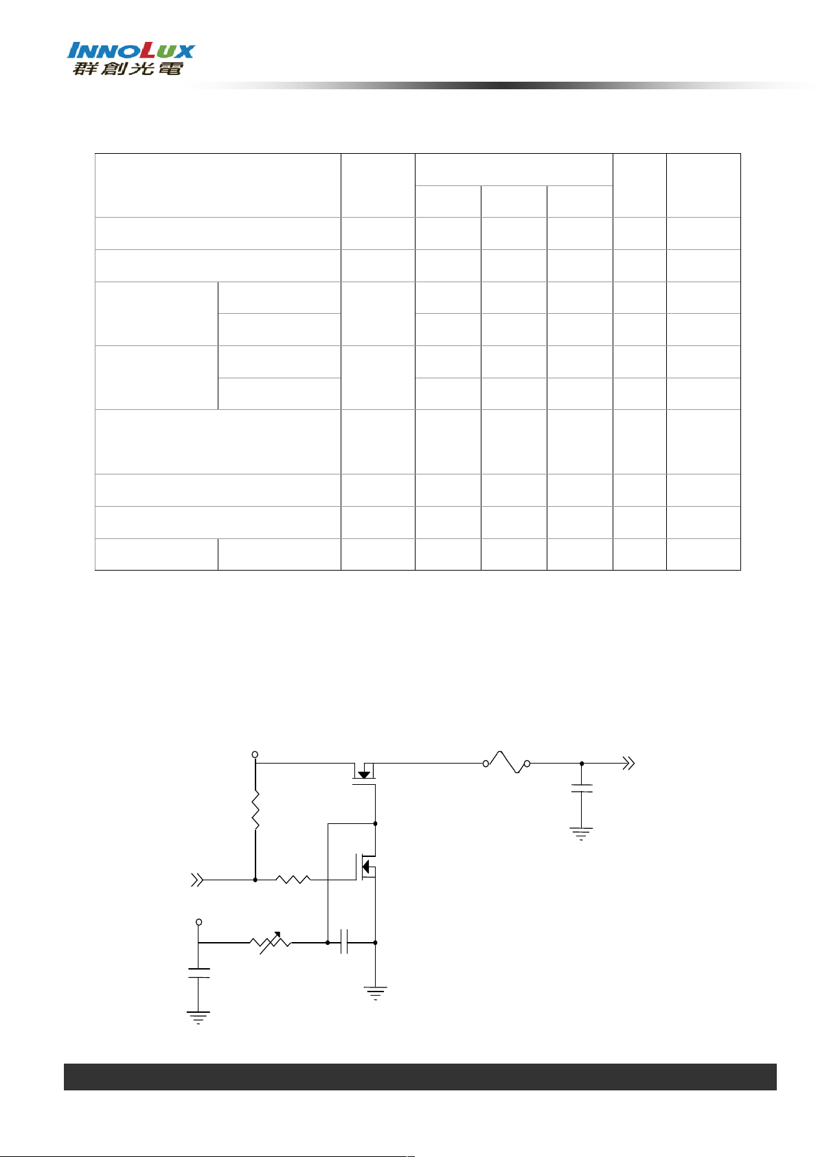
Measurement Conditions: Shown as the following figure. Test pattern: black.
(High to Low)
(Control Signal)
SW
+12V
+3.3V
R1
47K
R2
1K
47K
VR1
C1
1uF
Q1 2SK1475
0.01uF
Q2
2SK1470
FUSE
C3
1uF
VCCS
(LCD Module Input)
VCCS rising time is 0.5ms
Version 1.1 1 March 2013 9 / 37
The copyright belongs to InnoLux. Any unauthorized use is prohibited.

PRODUCT SPECIFICATION
Note (3) The specified power supply current is under the conditions at VCCS = 3.3 V, Ta = 25 ± 2 ºC, DC
Current and fv = 60 Hz, whereas a power dissipation check pattern below is displayed.
a. Mosaic Pattern
Active Area
Version 1.1 1 March 2013 10 / 37
The copyright belongs to InnoLux. Any unauthorized use is prohibited.
PRODUCT SPECIFICATION
PWM Control Permissive Ripple
C2
4.3.2 LED CONVERTER SPECIFICATION
Parameter Symbol
Value
Unit Note
Min. Typ. Max.
Converter Input power supply voltage
Converter Inrush Current
LED_Vccs
ILED
RUSH
(5.0) (12.0) (21.0) V
- - (1.5) A (1)
Backlight On (2.2) - (5) V
EN Control Level
Backlight Off
PWM High Level
PWM Control Level
PWM Low Level
(0) - (0.6) V
(2.2) - (5) V
(0) - (0.6) V
PWM Control Duty Ratio (5) - (100) %
Voltage
PWM Control Frequency f
LED Power Current LED_VCCS =Typ.
Note (1) ILED
: the maximum current when LED_VCCS is rising,
RUSH
(190) - (2K) Hz (2)
PWM
ILED (116) (145) (163) mA (3)
- - (100) mV
V
PWM_pp
ILEDIS: the maximum current of the first 100ms after power-on,
Measurement Conditions: Shown as the following figure. LED_VCCS = Typ, Ta = 25 ± 2 ºC, f
= 200 Hz, Duty=100%.
.
LED_VCCS(Typ)
Q1 IRL3303
(High to Low)
(Control Signal)
SW=24V
LED_VCCS(Typ)
C1
1uF
R1
47K
R2
1K
Q2
IRL3303
47K
VR1
0.01uF
FUSE
C3
1uF
(LED Converter Input)
PWM
Version 1.1 1 March 2013 11 / 37
The copyright belongs to InnoLux. Any unauthorized use is prohibited.

PRODUCT SPECIFICATION
≤∗+
∗+≤
≥
VLED rising time is 0.5ms
0.5ms
90%
ILED
10%
Rush
100ms
ILED
IS
LED_VCC
LED_PWM
LED_EN
ILED
Note (3) If PWM control frequency is applied in the range less than 1KHz, the “waterfall” phenomenon on
the screen may be found. To avoid the issue, it’s a suggestion that PWM control frequency should
follow the criterion as below.
0V
0V
0V
PWM control frequency f
fN )33.0(
N
: Integer
f
: Frame rate
Note (4) The specified LED power supply current is under the conditions at “LED_VCCS = Typ.”, Ta = 25
± 2 ºC, f
= 200 Hz, Duty=100%.
PWM
should be in the range
PWM
f
PWM
)3(
N
fN
)66.0(
Version 1.1 1 March 2013 12 / 37
The copyright belongs to InnoLux. Any unauthorized use is prohibited.
 Loading...