

chimei N156B6-L0A Datasheet
Dcc No.:400040432
Issued Date: Jun,24, 2010
Model No.: N156B6-L0A
Approval
TFT LCD Approval Specification
MODEL NO.: N156B6-L0A
Customer : ____
Approved by :
Note :
核准時間 部門 審核 角色 投票
楊
NB
2010-06-28
14:23:38
產品管理處
2010.06.28
竣 傑
1 / 33
Director Accept
Version 2.1

Dcc No.:400040432
Issued Date: Jun,24, 2010
Model No.: N156B6-L0A
Approval
- CONTENTS -
REVISION HISTORY ------------------------------------------------------- 3
1. GENERAL DESCRIPTION
1.1 OVERVIEW
1.2 FEATURES
1.3 APPLICATION
1.4 GENERAL SPECIFICATIONS
1.5 MECHANICAL SPECIFICATIONS
2. ABSOLUTE MAXIMUM RATINGS
2.1 ABSOLUTE RATINGS OF ENVIRONMENT
2.2 ELECTRICAL ABSOLUTE RATINGS
3. ELECTRICAL CHARACTERISTICS
3.1 TFT LCD MODULE
3.2 BACKLIGHT UNIT
4. BLOCK DIAGRAM
4.1 TFT LCD MODULE
5. INPUT TERMINAL PIN ASSIGNMENT
5.1 TFT LCD MODULE
5.2 TIMING DIAGRAM OF LVDS INPUT SIGNAL
5.3 COLOR DAT A INPUT ASSIGNMENT
5.4 EDID DATA STRUCTURE
6. CONVERTER
6.1 ABSOLUTE MAXIMUM RATINGS
6.2 RECOMMENDED OPERATING RATINGS
7. INTERFACE TIMING
7.1 INPUT SIGNAL TIMING SPECIFICATIONS
7.2 POWER ON/OFF SEQUENCE
8. OPTICAL CHARACTERISTICS
8.1 TEST CONDITIONS
8.2 OPTICAL SPECIFICATIONS
9. PRECAUTIONS
9.1 HANDLING PRECAUTIONS
9.2 STORAGE PRECAUTIONS
9.3 OPERATION PRECAUTIONS
10. PACKING ------------------------------------------------------- 29
10.1 CARTON
10.2 PALLET
11. DEFINITION OF LABELS
11.1 CMO MODULE LABEL
11.2 CARTON LABEL
12. MECHANICAL DRAWING
------------------------------------------------------- 4
------------------------------------------------------- 5
------------------------------------------------------- 7
------------------------------------------------------- 11
------------------------------------------------------- 12
------------------------------------------------------- 19
------------------------------------------------------- 21
------------------------------------------------------- 24
------------------------------------------------------- 28
------------------------------------------------------- 31
------------------------------------------------------- 33
2 / 33
Version 2.1
Dcc No.:400040432
Issued Date: Jun,24, 2010
Model No.: N156B6-L0A
Approval
Version Date
Ver. 2.0
Ver.2.1
Dec.24, 2009
May.31,2010
Page
(New)
All
10
REVISION HISTORY
Section Description
Approval spec 2.0 was first issued for N156B6-L0B.
All
p.28
Approval spec 2.1 was updated for packing.
3 / 33
Version 2.1
Dcc No.:400040432
Issued Date: Jun,24, 2010
Model No.: N156B6-L0A
1. GENERAL DESCRIPTION
1.1 OVERVIEW
N156B6-L0B is a 15.6” (15.547” diagonal) TFT Liquid Crystal Display module with LED Backlight unit and
40 pins LVDS interface. This module supports 1366 x 768 HD mode and can display 262,144 colors. The
optimum viewing angle is at 6 o’clock direction.
1.2 FEATURES
- HD (1366 x 768 pixels) resolution
- 3.3V LVDS (Low Voltage Differential Signaling) interface with 1 pixel/clock
- WLED
- LED converter embedded
1.3 APPLICA TION
Approval
- TFT LCD Notebook
1.4 GENERAL SPECIFICATI0NS
Item Specification Unit Note
Active Area 344.232 (H) x 193.536 (V) (15.547” diagonal) mm
Bezel Opening Area 349.58 (H) x 198.29 (V) mm
Driver Element a-si TFT active matrix - Pixel Number 1366 x R.G.B. x 768 pixel Pixel Pitch 0.252 (H) x 0.252 (V) mm Pixel Arrange ment RGB vertical stripe - Display Colors 262,144 color Transmissive Mode Normally white - Surface Treat ment Hard coating (3H), Glare - -
1.5 MECHANICAL SPECIFICATIONS
Item Min. Typ. Max. Unit Note
Horizontal(H) 358.8 359.3 359.8 mm
Module Size
Note (1) Please refer to the attached drawings for more information of front and back outline dimensions.
Vertical(V) 209 209.5 210 mm
Thickness(T) - 5.2 5.5 mm
Weight --- 430 445 g -
(1)
(1)
4 / 33
Version 2.1
Dcc No.:400040432
A
Issued Date: Jun,24, 2010
Model No.: N156B6-L0A
Approval
2. ABSOLUTE MAXIMUM RATINGS
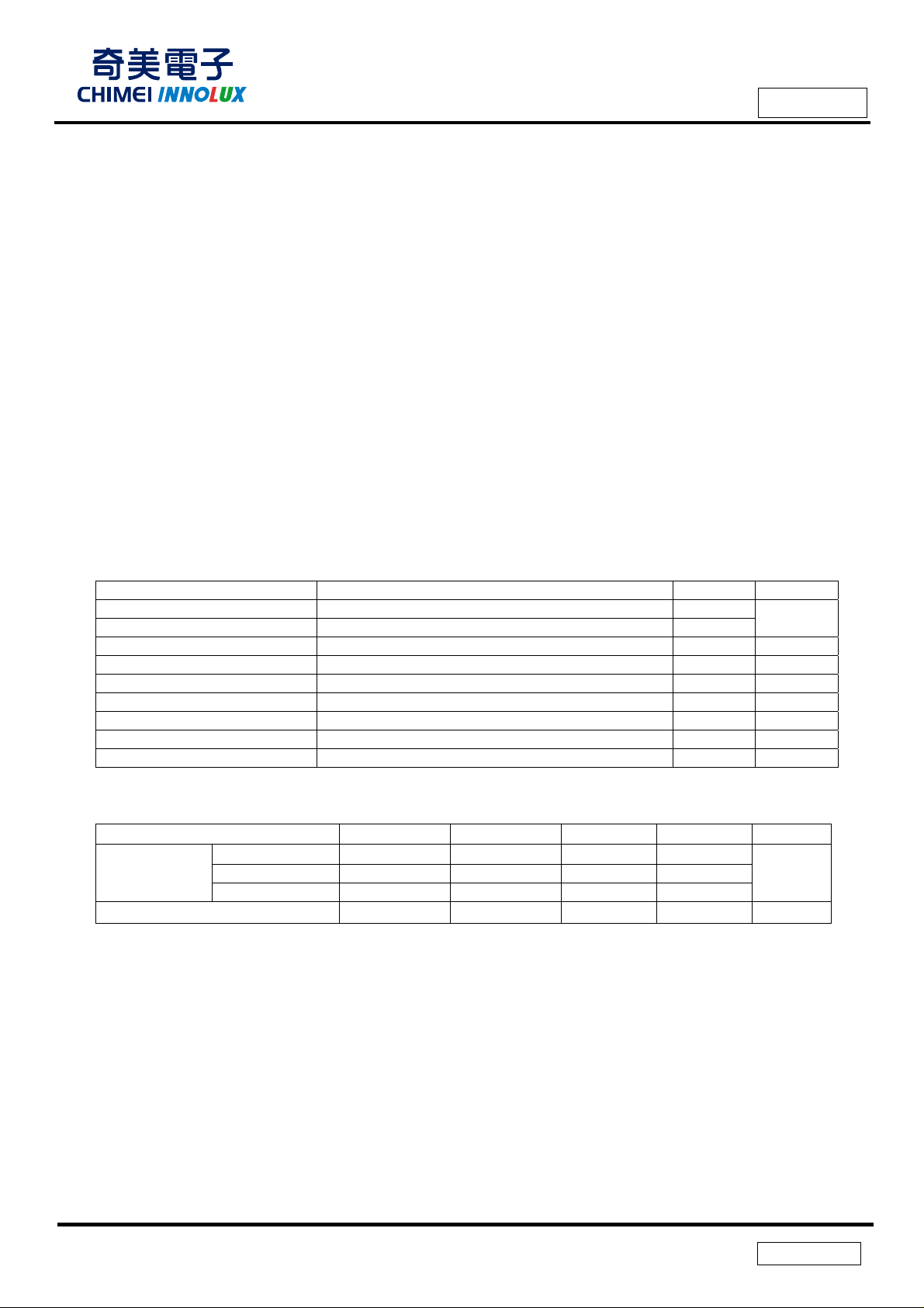
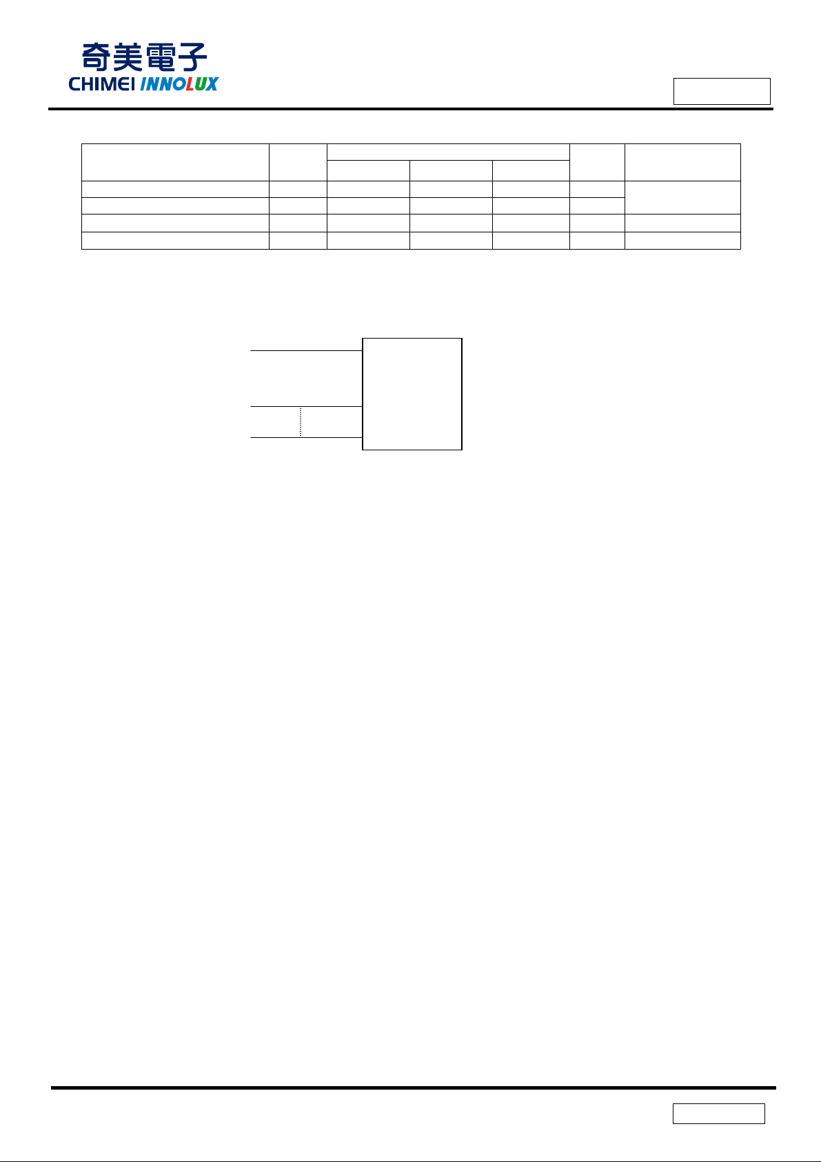
2.1 ABSOLUTE RATINGS OF ENVIRONMENT
Item Symbol
Storage Temperature TST -20 +60 ºC (1)
Operating Ambient T emperature TOP 0 +50 ºC (1), (2)
Shock (Non-Operating) S
Vibration (Non-Operating) V
Note (1) (a) 90 %RH Max. (Ta <= 40 ºC).
(b) Wet-bulb temperature should be 39 ºC Max. (Ta > 40 ºC).
(c) No condensation.
Note (2) The temperature of panel surface should be 0 ºC min. and 60 ºC max.
- 220/2 G/ms (3), (5)
NOP
- 1.5 G (4), (5)
NOP
Min. Max.
Relative Humidity (%RH)
100
90
Value
Unit Note
80
60
Operating Range
40
20
10
Storage Range
80 60 -20 40 0 20 -40
Temperature (ºC)
Note (3) 1 time for ± X, ± Y, ± Z. for Condition (220G / 2ms) is half Sine Wave,.
Note (4) 10~500 Hz, 0.5hr/cycle 1cycle for X,Y,Z
Note (5) At testing Vibration and Shock, the fixture in holding the module has to be hard and rigid
enough so that the module would not be twisted or bent by the fixture.
The fixing condition is shown as below:
t Room Temperature
Side Mount Fixing Screw
Gap=2mm
Bracket
LCD Module
Side Mount Fixing Screw
Stage
5 / 33
Version 2.1
Dcc No.:400040432
Issued Date: Jun,24, 2010
Model No.: N156B6-L0A
Approval
2.2 ELECTRICAL ABSOLUTE RATINGS
2.2.1 TFT LCD MODULE
Item Symbol
Power Supply V oltage VCCS -0.3 +4.0 V
Logic Input Voltage VI -0.3 VCCS+0.3 V
Note (1) Permanent damage to the device may occur if maximum values are exceeded. Function operation
should be restricted to the conditions described under Normal Operating Co nditions.
Min. Max.
2.2.2 BACKLIGHT UNIT
Item
LED Light Bar Power Supply Voltage -40 28 VDC
LED Light Bar Power Supply Current 0 150 mADC
Note (1) Permanent damage to the device may occur if maximum values are exceeded. Function operation
Min Max.
Value
Value
Unit Note
(1)
Unit Note
(1), (2)
should be restricted to the conditions described under Normal Operating Co nditions.
Note (2) Specified values are for LED (Refer to Section 3.2 for further information).
6 / 33
Version 2.1
Dcc No.:400040432
Issued Date: Jun,24, 2010
Model No.: N156B6-L0A
Approval
3. ELECTRICAL CHARACTERISTICS
3.1 TFT LCD MODULE Ta = 25 ± 2 ºC
Parameter Symbol
Min. Typ. Max.
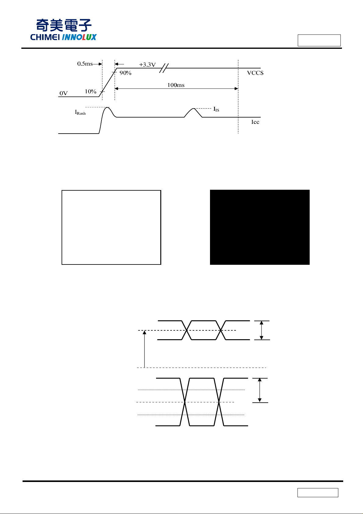
Power Supply V oltage VCCS 3.0 3.3 3.6 V Ripple Voltage VRP - 50 - mV Rush Current I
- - 1.5 A (2)
RUSH
Initial Stage Current IIS - - 1.0 A (2)
Power Supply Current
LVDS Differential Input High Threshold V
LVDS Differential Input Low Threshold V
White 185 215 245 (3)a (3)a
Black
lcc
TH(LVDS)
TL(LVDS)
320 360 400 (3)b (3)b
- - +100 mV
-100 - - mV
LVDS Common Mode Voltage VCM 1.125 - 1.375 V (4)
LVDS Differential Input Voltage |VID| 100 - 600 mV (4)
Terminating Resistor RT - 100 - Ohm -
Power per EBL WG PEBL - 1.97 W (5)
Note (1) The ambient temperature is Ta = 25 ± 2 ºC.
Value
Unit Note
V
CM
V
CM
(4),
=1.2V
(4)
=1.2V
Note (2) I
: the maximum current when VCCS is rising
RUSH
I
: the maximum current of the first 100ms after power-on
IS
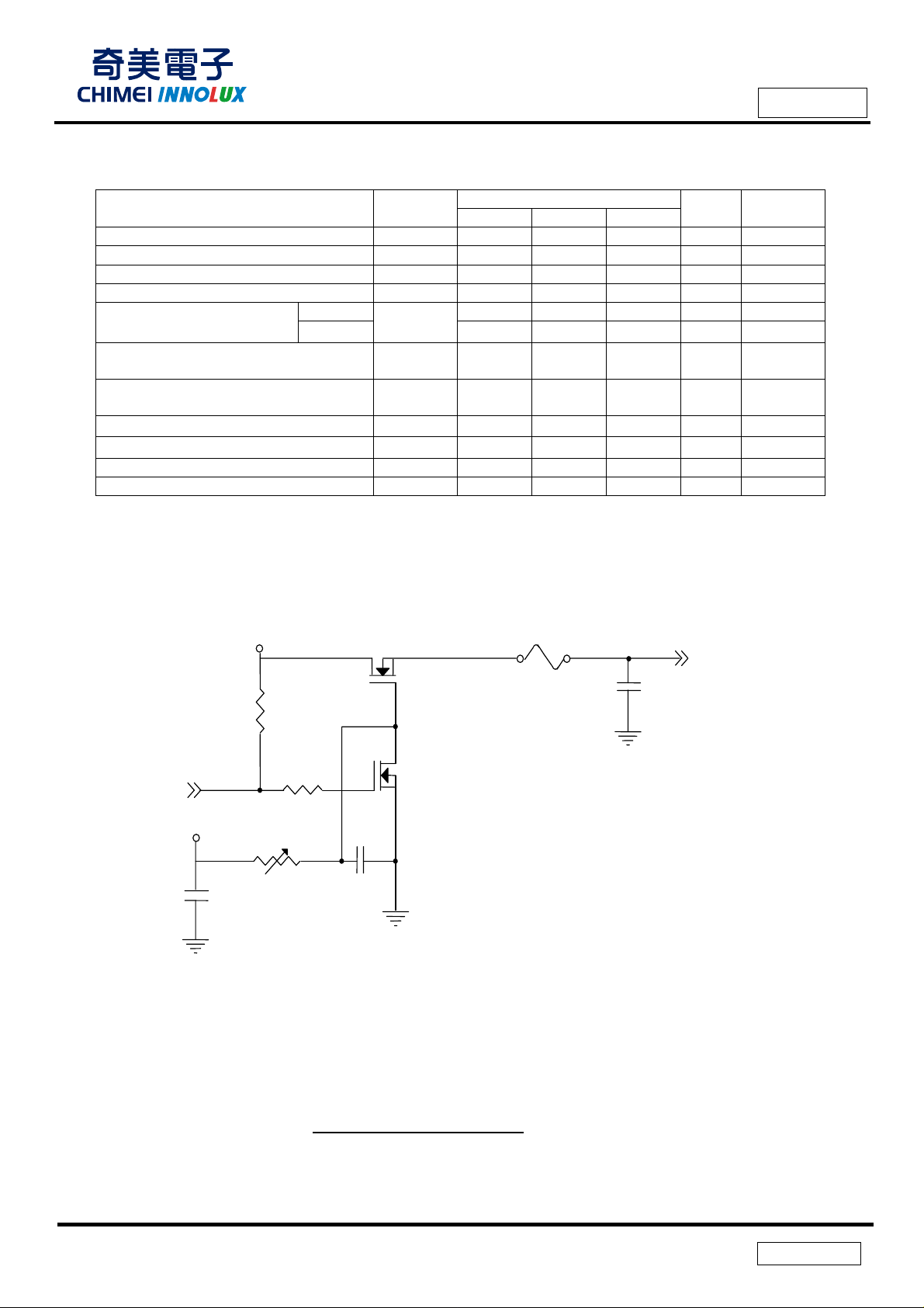
Measurement Conditions: Shown as the following figure. Test pattern: black.
+3.3V
Q1 2SK1475
VR1
R1
47K
47K
R2
1K
Q2
2SK1470
C2
0.01uF
(High to Low)
(Control Signal)
SW
+12V
C1
1uF
FUSE
C3
1uF
VCCS
(LCD Module Input)
VCCS rising time is 0.5ms
7 / 33
Version 2.1
Dcc No.:400040432
|
|
Issued Date: Jun,24, 2010
Model No.: N156B6-L0A
Approval
Note (3) The specified power supply current is under the conditions at VCCS = 3.3 V, Ta = 25 ± 2 ºC, DC
Current and f
Note (4) The parameters of LVDS signals are defined as the following figures.
a. White Pattern
Single Ended
= 60 Hz, whereas a power dissipation check pattern below is displayed.
v
b. Black Pattern
Active Area
CM
V
Active Area
VID|
Note (5) The specified power are the sum of LCD panel electronics input power and the converter input
Differential
V
V
0V
VID|
0V
8 / 33
Version 2.1
power. Test conditions are as follows.
Dcc No.:400040432
Issued Date: Jun,24, 2010
Model No.: N156B6-L0A
Approval
(a) VCCS = 3.3 V, Ta = 25 ± 2 ºC, f
(b) The pattern used is a black and white 32 x 36 checkerboard, s lide #100 from the VESA fil e
“Flat Panel Display Monitor Setup Patterns”, FPDMSU.ppt.
(c) Luminance: 60 nits.
= 60 Hz,
v
9 / 33
Version 2.1
Dcc No.:400040432
Issued Date: Jun,24, 2010
Model No.: N156B6-L0A
Approval
3.2 BACKLIGHT UNIT Ta = 25 ± 2 ºC
Parameter Symbol
LED Light Bar input Voltage V
L
Min. Typ. Max.
22.4 25.6 27.2 V
LED Light Bar input Current IL 114 120 126 mA
Power Consumption PL 2.55 3.07 3.43 W (3) Duty=100%
LED Life Time LBL 15000 Hrs (4)
Note (1) LED light bar configuration is shown as below.
V
Light Bar Feedback
Channels
L, IL
LED
Light Bar
Value
Unit Note
(1) Duty 100%
Note (2) For better LED light bar driving quality, it is recommended to utilize the adaptive boost converter
with current balancing function to drive LED light-bar.
Note (3) P
= IL × V
L
L
Note (4) The lifetime of LED is defined as the time when it continues to operate under the conditions at Ta =
o
25 ± 2
C and IL = 24.0mA (Per EA) until the brightness becomes 50% of its original value.≦
10 / 33
Version 2.1
 Loading...