

CHI MEI N150X3-L09 User Manual
RGB ELEKTRONIKA AGACIAK CIACIEK
SPÓŁKA JAWNA
Jana Dlugosza 2-6 Street
51-162 Wrocław
Poland
biuro@rgbelektronika.pl
+48 71 325 15 05
www.rgbautomatyka.pl
www.rgbelektronika.pl
DATASHEET
www.rgbautomatyka.pl
www.rgbelektronika.pl
OTHER SYMBOLS:
N150X3-L09
N150X3L09, N150X3 L09, N150X3-L09
CHI MEI
YOUR
PARTNER IN
MAINTENANCE
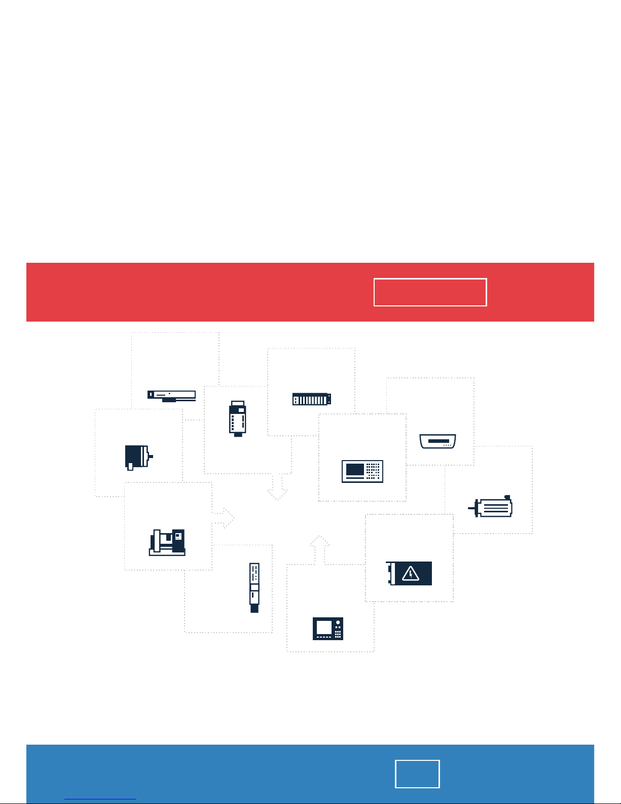
At our premises in Wrocław, we have a fully equipped servicing facility. Here we perform all the repair
works and test each later sold unit. Our trained employees, equipped with a wide variety of tools and
having several testing stands at their disposal, are a guarantee of the highest quality service.
OUR SERVICES
ENCODERS
SERVO
DRIVERS
LINEAR
ENCODERS
SERVO AMPLIFIERS
CNC
MACHINES
MOTORS
POWER
SUPPLIERS
OPERATOR
PANELS
CNC
CONTROLS
INDUSTRIAL
COMPUTERS
PLC
SYSTEMS
Repair this product with RGB ELEKTRONIKA
ORDER A DIAGNOSIS
∠
Buy this product at RGB AUTOMATYKA
BUY
∠

www.DataSheet.net/
Datasheet pdf - http://www.DataSheet4U.co.kr/

Issued Date: Sep.27, 2005
Model No.: N150X3 - L09
Approval
2 / 27
Version 2.2
- CONTENTS -
REVISION HISTORY ------------------------------------------------------- 3
1. GENERAL DESCRIPTION ------------------------------------------------------- 4
1.1 OVERVIEW
1.2 FEATURES
1.3 APPLICATION
1.4 GENERAL SPECIFICATIONS
1.5 MECHANICAL SPECIFICATIONS
2. ABSOLUTE MAXIMUM RATINGS ------------------------------------------------------- 5
2.1 ABSOLUTE RATINGS OF ENVIRONMENT
2.2 ELECTRICAL ABSOLUTE RATINGS
2.2.1 TFT LCD MODULE
2.2.2 BACKLIGHT UNIT
3. ELECTRICAL CHARACTERISTICS ------------------------------------------------------- 6
3.1 TFT LCD MODULE
3.2 BACKLIGHT UNIT
3.3 EDID DATA
4. BLOCK DIAGRAM ------------------------------------------------------- 13
TFT LCD MODULE w/ INVERTER
5. INPUT TERMINAL PIN ASSIGNMENT ------------------------------------------------------- 13
5.1 TFT LCD MODULE
5.2 TIMING DIAGRAM OF LVDS INPUT SIGNAL
5.3 COLOR DATA INPUT ASSIGNMENT
6. INTERFACE TIMING ------------------------------------------------------- 16
6.1 INPUT SIGNAL TIMING SPECIFICATIONS
6.2 POWER ON/OFF SEQUENCE
7. OPTICAL CHARACTERISTICS ------------------------------------------------------- 18
7.1 TEST CONDITIONS
7.2 OPTICAL SPECIFICATIONS
8. PRECAUTIONS ------------------------------------------------------- 23
8.1 ASSEMBLY AND HANDLING PRECAUTIONS
8.2 SAFETY PRECAUTIONS
9. DEFINITION OF LABELS ------------------------------------------------------- 24
9.1 CMO MODULE LABEL
9.2 Dell LABEL
10.2.1 MAL PPID LABEL
10.2.2 CARTON LABEL
10.2.3 PALLET LABEL
10. PACKING ------------------------------------------------ 25
10.1 CARTON
10.2 PALLET
www.DataSheet.net/
Datasheet pdf - http://www.DataSheet4U.co.kr/

Issued Date: Sep.27, 2005
Model No.: N150X3 - L09
Approval
3 / 27
Version 2.2
REVISION HISTORY
Version Date
Page
(New)
Section Description
Ver 1.0
Ver 2.0
Ver 2.1
Ver 2.2
Jan.31 ‘05
May.23 ’05
Aug.31 ‘05
Sep 27,’05
All
9
25
14
15
All
3.3
10
4.2
5.1
Perminaliary specification was first issued
Added EDID code
Modified Carton & pallet
Added 4.2 BLU unit
Modified pin assignment
www.DataSheet.net/
Datasheet pdf - http://www.DataSheet4U.co.kr/
Issued Date: Sep.27, 2005
Model No.: N150X3 - L09
Approval
4 / 27
Version 2.2
1. GENERAL DESCRIPTION
1.1 OVERVIEW
N150X3- L09 is a 15.0” TFT Liquid Crystal Display module. This module supports 1024 x 768 XGA mode
and can display 262,144 colors. The optimum viewing angle is at 6 o’clock direction.
1.2 FEATURES
- Thin and Light Weight
- XGA (1024 x 768 pixels) resolution
- DE only mode
- 3.3V LVDS (Low Voltage Differential Signaling) interface with 1 pixel/clock
- SPWG (Standard Panel Working Group) Style B compatible
- Single CCFL
- ROHS product
1.3 APPLICATION
- TFT LCD Notebook
1.4 GENERAL SPECIFICATI0NS
Item Specification Unit Note
Active Area 304.1 (H) x 228.1 (V) (15.0” diagonal) mm
Bezel Opening Area 307.8 (H) x 231.6 (V) mm
(1)
Driver Element a-si TFT active matrix - Pixel Number 1024 x R.G.B. x 768 pixel Pixel Pitch 0.297 (H) x 0.297 (V) mm Pixel Arrangement RGB vertical stripe - Display Colors 262,144 color Transmissive Mode Normally white - Surface Treatment Hard coating (3H), Anti-glare (Haze 25) - -
1.5 MECHANICAL SPECIFICATIONS
Item Min. Typ. Max. Unit Note
Horizontal(H) 316.8 317.3 317.8 mm (1)
Vertical(V) 241.5 242 242.5 mm (1)
Module Size
Depth(D) - 5.7 6.0 mm (1)
Weight - 550 565 g -
Note (1) Please refer to the attached drawings for more information of front and back outline dimensions.
www.DataSheet.net/
Datasheet pdf - http://www.DataSheet4U.co.kr/
Issued Date: Sep.27, 2005
Model No.: N150X3 - L09
Approval
5 / 27
Version 2.2
2. ABSOLUTE MAXIMUM RATINGS
2.1 ABSOLUTE RATINGS OF ENVIRONMENT
Value
Item Symbol
Min. Max.
Unit Note
Storage Temperature TST -20 +60 ºC (1)
Storage Humidity HST 10 90 %RH (1)
Operating Ambient Temperature TOP 0 +50 ºC (1), (2)
Operating Ambient Humidity HOP 20 90 %RH (1)
Shock (Non-Operating) S
NOP
- 200/2 G/ms (3), (4), (5)
Vibration (Non-Operating) V
NOP
- 1.5/10-200 G/Hz (4), (5)
Note (1) (a) 90 %RH Max. (Ta ≦ 40 ºC).
(b) Wet-bulb temperature should be 39 ºC Max. (Ta > 40 ºC).
(c) No condensation.
Note (2) The temperature of panel surface should be 0℃ min. and 50 ℃ max.
Note (3) Condition for 200/2 G/ms is Half Since Wave.
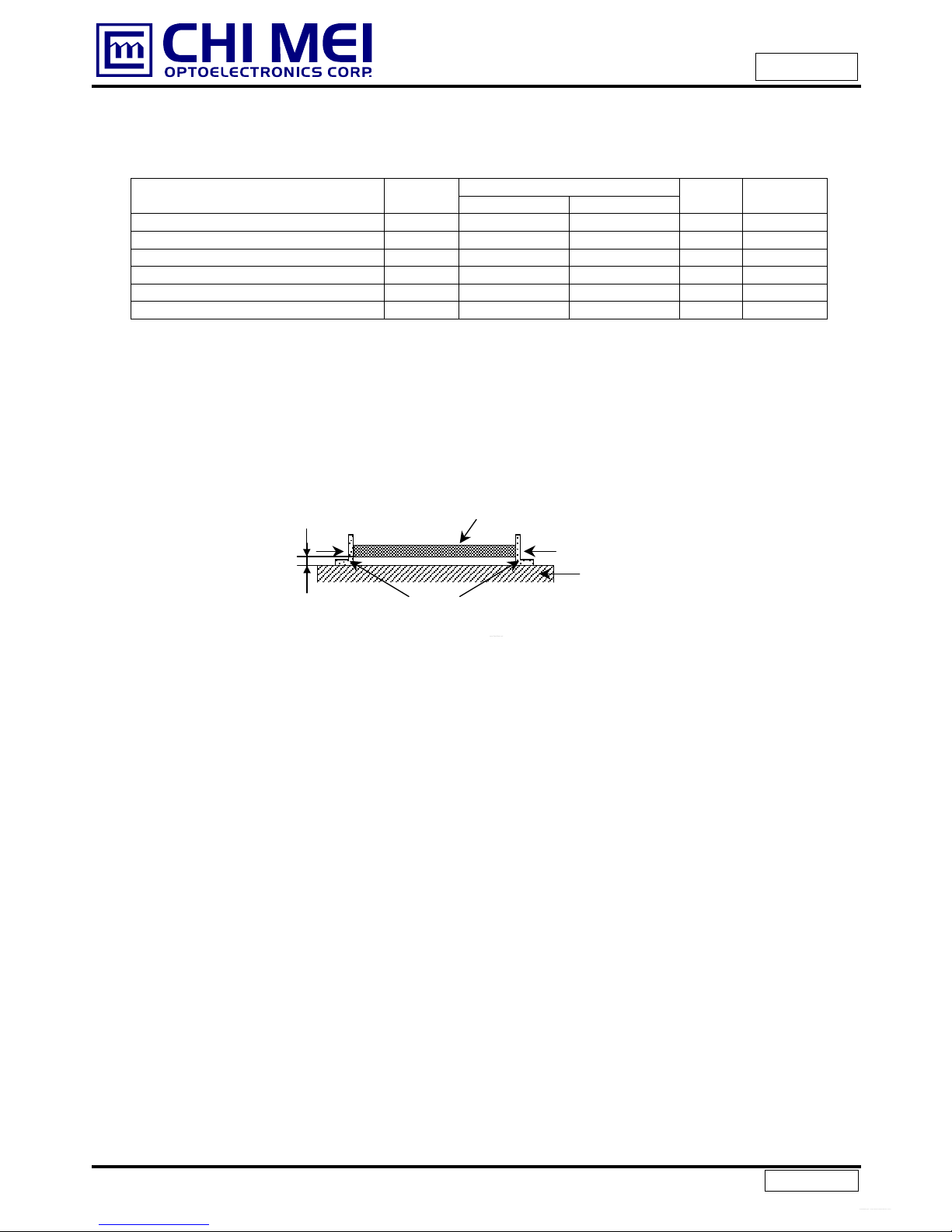
Note (4) The fixing condition is shown as below:
Note (5) At testing Vibration and Shock, the fixture in holding the module has to be hard and rigid enough
so that the module would not be twisted or bent by the fixture.
Side Mount Fixing Screw
Side Mount Fixing Screw
Stage
Bracket
LCD Module
gap=2mm
www.DataSheet.net/
Datasheet pdf - http://www.DataSheet4U.co.kr/
Issued Date: Sep.27, 2005
Model No.: N150X3 - L09
Approval
6 / 27
Version 2.2
2.2 ELECTRICAL ABSOLUTE RATINGS
2.2.1 TFT LCD MODULE
Value
Item Symbol
Min. Max.
Unit Note
Power Supply Voltage VCC -0.3 +4.0 V
Logic Input Voltage VIN -0.3 VCC+0.3 V
(1)
2.2.2 BACKLIGHT UNIT
Value
Item Symbol
Min. Max.
Unit Note
Lamp Voltage VL - (2.5K) V
RMS
(1), (2), IL = 6.0 mA
Lamp Current IL 2.0 6.5 mA
RMS
Lamp Frequency FL 50 80 KHz
(1), (2)
Note (1) Permanent damage to the device may occur if maximum values are exceeded. Function operation
should be restricted to the conditions described under Normal Operating Conditions.
Note (2) Specified values are for lamp (Refer to 3.2 for further information).
3. ELECTRICAL CHARACTERISTICS
3.1 TFT LCD MODULE Ta = 25 ± 2 ºC
Value
Parameter Symbol
Min. Typ. Max.
Unit Note
Power Supply Voltage Vcc 3.0 3.3 3.6 V Ripple Voltage VRP - 100 - mV Rush Current I
RUSH
- - 1.5 A (2)
White - 300 350 mA (3)a
Power Supply Current
Black
Lcc
- 350 400 mA (3)b
“H” Level VIL - - +100 mV - Logical Input Voltage
(LVDS)
“L” Level V
IH
-100 - - mV Terminating Resistor RT - 100 - Ohm Power per EBL WG P
EBL
- 3.224 - W (4)
Note (1) The module should be always operated within above ranges.
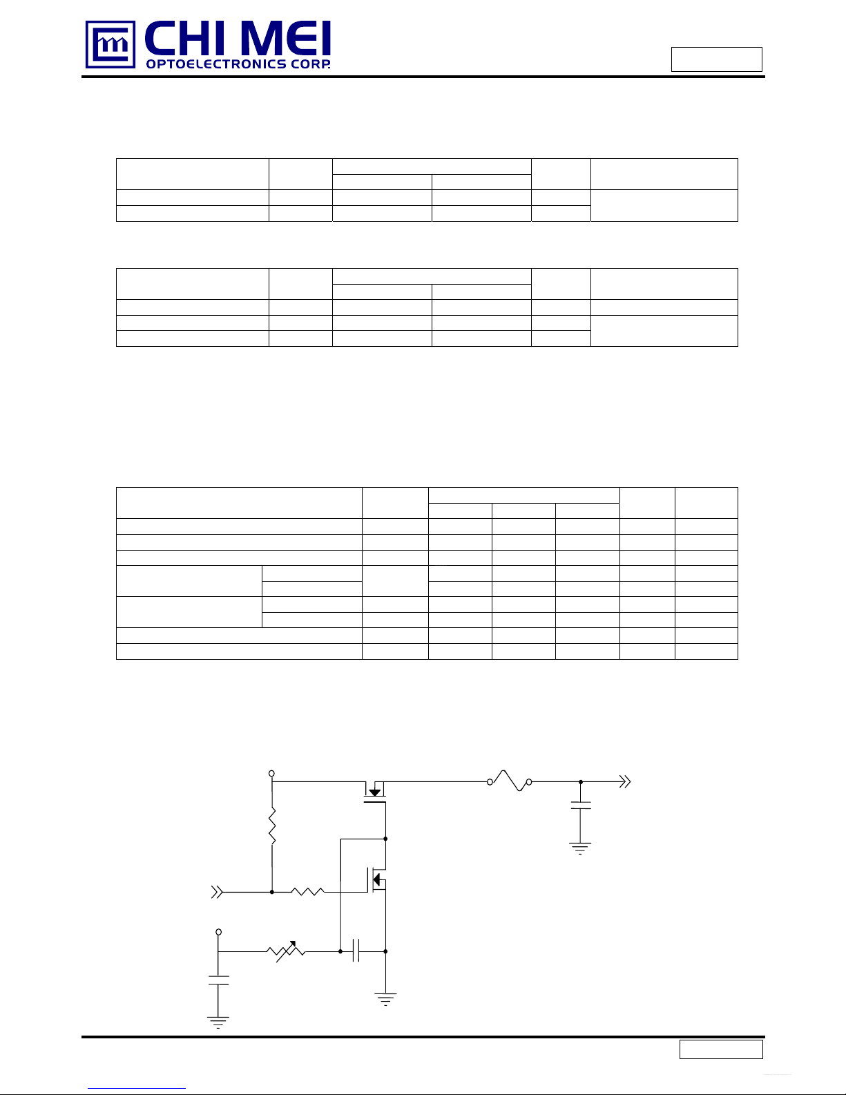
Note (2) Measurement Conditions:
R1
(High to Low)
(Control Signal)
+12V
SW
Q2
C1
1uF
Vcc
+3.3V
2SK1470
Q1 2SK1475
47K
R2
1K
VR1
47K
C2
0.01uF
C3
1uF
FUSE
(LCD Module Input)
www.DataSheet.net/
Datasheet pdf - http://www.DataSheet4U.co.kr/
Issued Date: Sep.27, 2005
Model No.: N150X3 - L09
Approval
7 / 27
Version 2.2
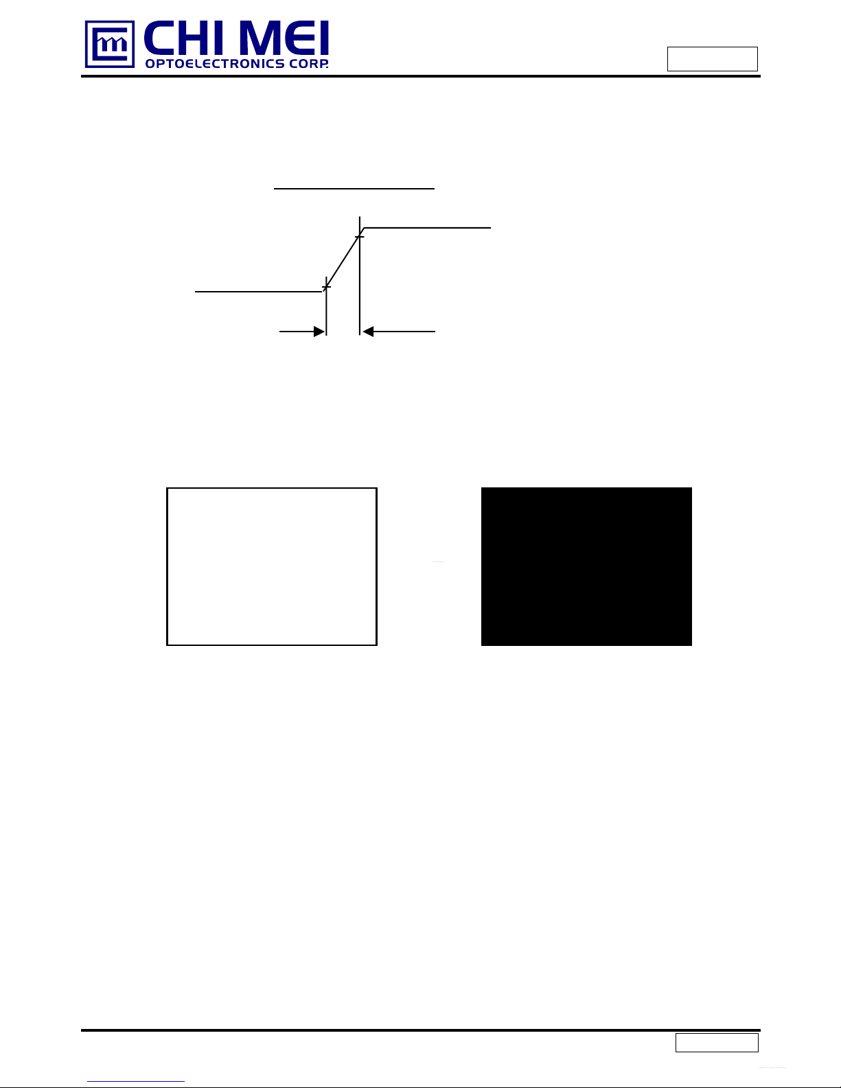
Note (3) The specified power supply current is under the conditions at Vcc = 3.3 V, Ta = 25 ± 2 ºC, f
v
= 60
Hz, whereas a power dissipation check pattern below is displayed.
Note (4) The specified power are the sum of LCD panel electronics input power and the inverter input
power. Test conditions are as follows.
(a) Vcc = 3.3 V, Ta = 25 ± 2 ºC, f
v
= 60 Hz,
(b) The pattern used is a black and white 32 x 36 checkerboard, slide #100 from the VESA file
“Flat Panel Display Monitor Setup Patterns”, FPDMSU.ppt.
(c) Luminance: 60 nits.
(d) The inverter used is provided from O2Micro (www.o2micro.com). Please contact O2Mirco for detail
information. CMO doesn’t provide the inverter in this product.
Vcc rising time is 470µs
470µs
+3.3V
GND
0.9Vcc
0.1Vcc
Active Area
a. White Pattern
Active Area
b. Black Pattern
www.DataSheet.net/
Datasheet pdf - http://www.DataSheet4U.co.kr/
 Loading...