

Page 1
100%
<="
€>
CH-498B
Motherboard
User’s
Manual
252-00498-C01
September,
1994
Printed
in
Thailand
Page 2
1.
Introduction
Mainboard
2.
Hardware
CONMECIOLS
JUMNIPETS.
DRAM
Hardware
3.
Green
CPU
VGA
IDE
External
Specification
..........
Description
«6
s:0incon
cine
cs
sesce
ess
A.
B.
C.
D.
E.
F.
G.
H.
I.
J.
K.
L.
sess
Cache
Size
Selection:
Voltage
Adjustment
5V/3.3V
Voltage
JP12:
CMOS
Powergood
CPU
VL-Bus
CPU
CPU
VL-Bus
Reserved
Bank
Selection:
Reserved
Function,
Data
Clear
(JP13)
Signal
Selection:
Clock
Selection
Targets
High
Clock
Selection:
Type
Selection:
Operation
Clock
Function:
Configuration............
or
Software
Speed
Function
Power
Down
Control
For
SMI
Green
(can
Normal
Down
Device
Down
Green
Control.
Control
Power
stop
(can’t
Down
For
Power
Power
Table
00...
eee c cece
eseonaaeraas
meme
ss
sumemecess
(IPO ~ JP7)
for
(JP15)..........
Speed
(JP17~JP20)
(JP21~JP29)
(JP31~JP33)..........
...........
clock
stop
............
............0
yb
soemaTTSS
..........
3.3V
CPU:
(JP8)..............000
(JP9~JP11)
..................
Setting
is
Open.....................5.
........
0.00
cece
(JP14)..........
0006 c cence
write:
(JP16)....................55-
............
0.0.0...
Selection:
(JP30)..................+55-
00.0 c cece
Change
...................0
0.6
cece
CPU
series)
clock
CPU
series)
0c e cece
00
cece
Control.............0.6:e
of
Contents
eee
ener
eee
sseneser
arene
17560
RROET
EA
Reems
0...
cee
cc
cece
eee
0.
eee
200
eee
eee
eee
0.6
.c cc
eeeeee
eres
cece
eee
eens
00
cece
cece
eee
eee
eee
ees
0...
cece
cece
ee
eens
ccc
eee
eens
sees
eee
cee
cece
ence
eee
.....................55:
eee
eees
.................5.
eee
een
eee
eee
cence
eee
eens
cece
eee e ees
eee
1-2
2-1
2-3
2-3
2-3
2-4
2-4
2-4
2-4
2-4
2-4
2-4
2-5
2-6
2-6
2-6
2-6
3-1
3-1
3-2
3-2
3-2
3-2
Page 3
4.
WinBIOS
A.
B.
C.
D.
E.
Appendix
eee
PCB
Setup
a.
Standard
b.
Advanced
c.
Chipset
d.
Power
Utility
a.
Detect
By
CM
Security
Ba
I
By
Ct
Default
Exit
Setup
Layout
Setup
Window
Setup
Management
Window
C:
Bet
Window...
VES
Window.
0...
Placement
«2.2.0.0.
ecco
Setup.
Setup
00.0.0
cece.
Setup.....................................,
©0600.
and
Detect
Dr...
con
4
151
itinmenonsss4
+9
£¢8Réiwaasdnauancomermens....
sacnen
«4
ass»
0.0.0.0...
men
EEE
rersaaodoasy
2.0.2...
oc
11a
mn
remit:
41
Saebacecmentasccueues
sae
+
eeeampibissiammmmasmnnsegrcey
0k
oooocoecececee
ccc
ececcececeeeeceecec
0.0.
oeccececececceceeeee.
cece
cece.
ce
cee
cee
ce
ccceeceecece
cece.
cee.
ee.
i.
4-2
4-2
4-5
4-9
4-12
4-14
4-14
4-14
4-14
4-14
4-17
4-18
4-19
A-1
Chapter
Introduction
The
mainboard
is a 486-based
Three
VESA
slots
operation
in
high
and
And
numerous
And
introduction
performance,
so
on.
Dark
Green
work
frequency,
on
board
voltage
support
function
regulator
1
high
uses
is
PC/AT
performance
such
designed
different
support
system
as
OS/2,
+3.3V
and
add-on
Windows/386,
for
power
kinds
of
for
provides
cards,
saving.
CPU,
the
3.3V
Dark
Green
optimized
Windows
This
compatible
CPU
mainboard
for
series.
function.
for
running
3.1,
XENIX,
CPU
upgrade.
can
software
UNIX
provide
9-4
Page 4
Mainboard
CPU:
Frequency:
System
chipset:
Cache
size:
SRAM
type:
DRAM
size:
DRAM
type:
Slots:
Dark
Green
PCB:
Support
green
On
board
Hardware
Remark
If
the
i486DX4).
Specification
function:
power
supply
adjustable
voltage
suspend
switch
"*":
mainboard
INTEL
1486DX/DX2.
SL
enhanced
P24T
PGA
14860DX4
P24D
PGA
AMD
Am486DX/
CYRIX
Cx486DX/DX2
UMC
USS
Support
system
running
UMC
82C498,
82496.
Write
back
direct
64/128/256KB/512K/1MB
TAG
SRAM
8Kx8/16Kx8/32Kx8/64Kx8
DATA
SRAM
8Kx8/32Kx8/64Kx8/128Kx8.
Four
banks
of
mixed
to
128
MB.
Support
256Kx,
DRAM
chip.
Seven
16-bit
ISA
master
mode
slots,
IDE
Power
Down
VGA
Power
Down
External
Device
Power
CPU
stop
clock
CPU
slow
clock
(8
220 x 260
m/m, 4 layers
connector
for
regulator
for
supported
with
regulator
in
Q3
1480SX.
PGA
package
PGA — *
packag
DX2/DXLIDXL2
PGA
20/25/33/40/50
mapped
cache
selection.
72-pin
512Kx8,
1Mx1,
slots.
one
located
at
Down
MHz) — INTEL
controlling
3.3V
CPU
or
Q4,
then
1487SX
PGA
package.
(optional).
PGA
package
MHz.
with
size
and
30-
pin
SIMM
2Mx8,
4Mx1,
8-bit
ISA
slot.
ISA
slot
1,2,3.
INTEL
SL
enhanced.
Cyrix
Cx486DX/DX2.
i486SX/DX/DX2.
AMD
Am486DX/DX2/DXL/DXL2
UMC
U5S
the
AC
output
series
(e.g
i486DX4)
it
can
support
package.
of
three
power.
3.3V
package.
module
4Mx4,
VESA
CPU
of
16Mx1
(e.g.
Chapter
Hardware
Connector
In
this
chapter
help
you
or
make
up
an
Connectors
J1:
J2:
J3:
J4:
we
do
the
right
upgrade.
Keyboard
Power
Connector
On
board/External
Pin]
&4: e For
Pin
1:
Pin
4:
Pin 2 &
3:
2-3
short:
2-3
Open:
External
Pin
1-2:
Pin
1:
Pin
2:
Pin
3-4
Pin
3:
Pin
4:
and
will
setting
For
Connector
Device
2
describe
the
PCB
Description
Jumper
Settings
the
system
mainboard’s
of
this
board
whenever
Layout
Placement,
Battery
Connector
external
battery
Vde
Ground
On board
battery
enabled/disabled
Enabled
Disabled
Power
Down
Connector
For
external
device
Active
low
signal
external
low
device
signal
output
output
Ground
For
Active
Ground
|
2
pack
connectors
you
please
change
refer
to
and
the
the
jumpers.
system
Appendix.
That
will
configuration
CH-498B
Hardware
Description
Page 5
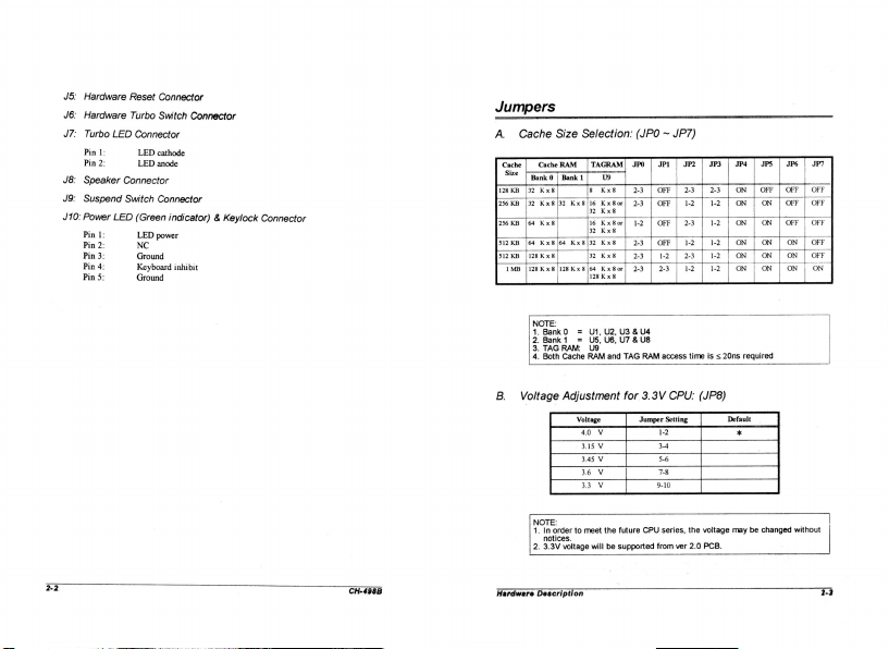
J5:
Hardware
Reset
2:
1:
2:
3:
4:
5:
1:
LED
Connector
Switch
LED
Turbo
Connector
LED
LED
(Green
LED
NC
Ground
Keyboard
Ground
Connector
Switch
cathode
anode
Connector
power
Connector
indicator) & Keylock
inhibit
Connector
CH-498B
J6:
Hardware
U7:
N
Turbo
Pin
Pin
J8:
Speaker
J9:
Suspend
J10:
Power
Pin
Pin
Pin
Pin
Pin
Jumpers
A.
Cache
Size
Selection:
(JPO ~ JP7)
Cache | CacheRAM
Size
128KB
256
KB
256KB
512KB
512KB
1MB
B.
Voltage
Hardware
|TAGRAM|
/Bank0
|]
Banki1|
[32
Kx8 8 Kx8 | 2-3 | OFF | 2-3 | 2-3 | ON | OFF | OFF | OFF
[32
Kx8|32
[64
Kx8
|64
Kx8l64
|128Kx8
128
Kx
8|128
NOTE:
1.
BankO = U1, U2,
3.
TAG
RAM:
4.
Both
Cache
Adjustment
NOTE:
1.
In
order
notices.
2.
3.3V
voltage
Description
JPO | JP1 | JP2 | JP3 | JP4 | JPS | JP6 | JP7
U9
Kx8|16
Kx8or|
2-3 | OFF | 1-2 | 1-2 | ON | ON | OFF | OFF
2
Kx8
16
Kx8or|
1-2 | OFF | 2-3 | 1-2 | ON | ON | OFF | OFF
32
Kx8
Kx8|32
Kx8 | 23 | OFF | 1-2 | 1-2 | ON | ON | ON | OFF
32
Kxs | 2-3 | 1-2 | 23 | 1-2 | ON | ON | ON | OFF
Kx
8/64
Kx
8or
23 | 23 | 12 | 1-2 | ON | ON | ON | ON
128Kx8&
=
US,
U6,
RAM
to
meet
the
will
U3 & U4
U7
&
U8
and
TAG
RAM
for
3.3V
future
CPU
be
supported
from
access
series,
time
is < 20ns
CPU:
(JP8)
the
voltage
ver
2.0
PCB.
Default
may
required
*
be
changed
without
|
Page 6
sh
S
>
D
=
wo
oO
Q
WwW
Ww
©
=
~z
2-4
9
©
®
Ss
oO
LJ
GS
a)
N
~H
O
Aa
ia
§
Qo
§
Ga
2a
..
9
yn
gid
Oo
qa
_.
{Ea
Oc
ZF,
>
mM
4
Qe”
28
a6
O
@
O
>
a=
Zee
Oo
23>
DM
|
PB
[I=
fafa
wo
>>|
{8
lo
|a
mn
*
wets
x
9
@
S
so‘!
Bo
Q
O<ee
©
6
®
e628
S42
25
°
FED
3
ol
G8
wm
=
D
9
oF
[US
©
3
38
Ss
58
B
&
3s
ys
¢s3cs
gy
x
—=
5
@
®
OBB
oO
&$3
2
&
O24
}
2]
s|
=
Ss
c
2
S
o
SS
@-2
leg2
=
S82
aes
Nw
..
Ss
S
o
~
S
S
9
&
©
8
se
no
23
ge
gr
ao
2
.¢
ke
>
—~
Stl]
®
oO
fo
i
i
S328
=
€nrneegqan
oA
rer
tse
®
S828
GBS
—$5
of
50
2
S
oO
z
2]
2
>
Ss
os
3
o
G
o
|
Ya
D
8B
ee
5
oo
5
~~
3S
3
fc
-.
£
5
3
§
So
cna
Ss
8s
Eg
o
«
<
Oo
&
oa
S
:
af
fe
=
§
fs)
®
3
=
a
8
2
,
&
—
[Zle
5]
iM
Y)
@
=
>
2
g@2o5
38
=
=
5
2
Doz
S
N
2
3
g
g&
oe
=
ed
o
.
3
35
i
>
a
j
+
+O
a
=
Q
vi
Hi—
Oo
2
wn
<
Q
+
=~
>
&&
35
3
=
3
s
=
~~
~
a
=
N
S
a\§a|iSsa
BIB
S/S
SIS
AIBAS
'
Te
&
a
°
®
~
~
~
[PI
&
Is
Y
(%
g
oO
23
as
Qa
Zz
5|
>|
3s
&
a
aloe
S
F
ss
Joe
88
SS
Sed
3
=
5
J.
CPU
Type
+—
—
a|x
A
x
c
2
FS
=
=
>
5
=
SH
Q
9
¢
x
3
A
Bs
é
5
3
3
Ss
S
o
¢
a
°
a
S
o
+
=
g
v
Ww
,
:
$
2
—
s
£
ie
a
o
:
CH-498B
Hardware
NadO
N3dO
NadO
NadO
vedr
6edr
2-1
z-1
e-2
e-2
N3dO
NadO
ede
S-p
s-p
p-e'z-t
p-e'2-1
NadO
NadO
Lede
|
p-e'e-1
NadO
ede
2-1
v-£
NadO
NadO
NadO
NadO
sede
vedr
2-4
€-2
€-2
2-1
NadO
NadO
NadO
NadO
ezdr
|
|
__-€'2-1
r-€'2-1
zedr
e-2
e-2
Nado_|1S-zxa/xager!
NadO
NadO
nado
lear
|
OOyaxager!
18-xS98P!
AdAL
XS98¢!
NdO
TEINI_|
73.LNI
TSLNI
T31NI
Description
Selection
NadO
Nado
z-t
s-p
yOOTO
ee
p-e'e-1
NdO
|
XE
pe'e-1
:
NAdO
Si
JO
ll
XZ
:
E-2
40
XG:
z
e-2
2-1
Nado
|
__
p-e'2-1
NadO
pXxC98b!
T3LNI
NadO
N3dO
|
S-r'2z-1
2-1
|
S-v'e-z
S-b
p-e'2-1
p-e'z-1
|
|
S-P'e-1
p-e'2-1
NadO
NadO
e-2
€-2
N3ad0
NadO
|
|
_¢-e'2-1
>-€'2-1
NadO
e-2
Qbéd
ved
T3LNI
TSN!
(JP21~JP29)
N3dO
NadO
NadO
NadO
|9-S‘p-e'2-1
]9-S'b-e'2-1
€-2
e-2
|
|
p-€'2-1
p-'2-1
NadO
NadO
NadO
NadO
e-2
e-2
|
|
p-€'2-1
p-e'2-1
NadO
v-£
NadO
NadO
Nado
NadO
e-2
z-t
Z-1
€-2
|9-s'p-e'2-1
|o-s'p-e'2-1
N3ad0
NadO
|
|
|
p-€'2-1
p-€'2-1
p-€'2-1
€-2
p-€'2-1
NadO
Nado
2-4
|z1xa/nxagerwy
ZXA98XO
XC9BPXO
ssn
XIHAD
XIHAD
own
aN
ae
ee
pe
e2|
N3dO
|
NadO
|
v-€
|
NadO
|
2-4
|
NadO
|
p-e'2-1
|
N3dO
pxageruy
anv
|
-FLON
ul
peyoddns
si
NdO
pxPespuy
“Lulg
seyiubis,
GV
eUL
M,“t
‘2
4@}&j
10
O'Z
UOISIBA
QOd
z@de
|.
vzar
|
szar
J]
czar
2-6
Page 7
K.
VL-Bus
Operation
Short:
Open:
L.
Reserved
Default
Setting
DRAM
Bank
There
are
two
72-pin
socket;
Guarantee
The
mainboard
will
memory
size
is
up
The
72-pin
SIMM
(RAS
pin = pin
34,
mode
is
required.
Hardware
The
mainboard
supports
changed
by
the
hardware
follows:
<ALT><CTRL><+> _ is
<ALT><CTRL><->_
If
the
turbo
switch
to
OFF,
the
system
set
to
HIGH
speed.
while
at
the
same
time
Clock
CPU
clock > 33
MHz
CPU
clock < 33
MHz
Function:
(JP31~JP33)
JP31:
Open
JP32:
2-3
JP33:
Short
Configuration
double-side
SIMM
the
DRAM
module
auto
detect
the
128
MB
socket
support
44
and
pin
Software
hardware
turbo
is
set
to
can
be
set
If
you
want
the
turbo
is
ON,
33,
switch
set
set
to
to
switch
the
high
total
single
45)
and
to
to
system
set
speed
to
or
Selection:
(Default)
sockets
installed
memory
bank
DRAM
module,
Speed
software
and
software
high
speed.
low
speed.
is
depending
the
system
must
also
set
(four
up
(RAS
speed
banks)
to
four
installed
pin = pin
the
changed
speed
to
low
on
to
HIGH
be
set
(JP30)
and one
banks
which
in
the
DRAM
Change
function.
is
changed
speed
or
the
software
speed
to
OFF.
SIMM
33,
module
if
with
bank
34)
by
the
are
and
of 80
Hardware
the
turbo
speed
the
of
30-pin
all
auto
socket.
double
ns
keyboard
switch
change
use
of
SIMM
banking.
The
total
banks
fast
page
speed
are
is
is
also
keyboard,
Chapter
Green
CPU
The
mainboard
supports
rate
on
standby
power
down
For
SM!
is
as
set
System
at
Power
two
timer
sequence
Green
Normal
Step
high
speed
i
Down
supports
to
set
mode.
are
(can
running
3
Function
Control
green
function
the
power
down
These.
function
as
follows:
stop
clock
Standby
ee
timeo
ie
ie | tep
System
at
low
t
1
for
the
system
saving
power.
The
system
stop
LED
Device
BIOS
be
set
to
low
clock
Setup.
The
|
|
off
*
off
*)
time.
The
CPU
clock
can
in
the
|
|
also
Power
Management
ane
ane
System
(Power
Monitor « off
IDE
o
peenal
are
included
CPU
series)
aaa
|
ae
spee
Green
Function
Page 8
For
Normal
VGA
The
mainboard
Management
Disabled:
Normal:
DPMS:
SMART:
IDE
The
mainboard
the
IDE
function,
External
The
mainboard
external
_
Enabled
function
detail
information,
3-2
Green
|
NOTE: * =
Power
Setup
Power
supports
power
the
IDE
supports
peripheral.
or
Disabled
CPU,
the
(can’t
stop
Normal
Step
System
running
at
high
speed
If
these
power
Down
supports
VGA
provides
Disabled/Normal/DPMS/SMART
Disable
the
function
Support
no
screen
For
VGA
card
BIOS
will
automatically
monitor
power
Down
IDE
power
down
control
setup
will
be
power
Device
Power
two
external
The
system
by
the
Power
external
device
please
refer
to
clock
Standby
timer
timeout
down
control
Control
power
down
mode
with
VESA
down mode
Control
down
enable
down.
device
BIOS
can
Management
power
down
chapter 2 for
CPU
control
but no
DPMS
detect
for
control
the
Down
for
set
the
Setup.
function
hardware
series)
Standby
Step
System
it 8 MHz
(Power
Monitor
IDE
off
External
functions
power
function.
the
power
to
system
power
external
running
LED
off
off
*
*
Device
are
to
set
monitor
saving
VGA
card
saving.
save
the
to
enter
Control
down
connector
device
If
the
system
is
always
connection
off)
enabled.
for
different
function.
type
IDE
power
the
power
uses
set
(J4).
to
then
power
to
(J4)
down
the
Enabled.
OFF,
the
VGA
card.
proceed
to
consumption.
management
to
control
function
non
stop
For
CH-498B
Power
the
clock
more
Chapter
WinBIOS
WinBIOS
Setup
has
had
used
interface.
Starting
As
POST
Hit
Press
<DEL>
The
WinBIOS
and
Default
activate a specific
follows:
If
the
to
WinBiOs
Setup
configures
an
easy-to-use
the
Microsoft
WinBlOS
executes,
<DEL>
to
run
Setup
four
Power
Mgmt
the
if
you
WinBIOS
main
windows.
function.
4
system
graphical
Windows.
Setup:
following
want
to
menu,
Each
The
Advanced
1
Setup
information
user
interface
WinBIOS
appears:
run
setup.
Setup.
shown
below,
window
contains
WinBIOS
Chipset
that
Setup
is
Setup
is
stored
that
is
sets a new
organized
several
icons
easily
into
icons,
and
in
CMOS
recognize
standard
Setup,
by
clicking
functions
RAM.
WinBIOS
by
anyone
in
BIOS
Utilities,
each
are
described
who
user
Security
icon
will
as
+1
Page 9
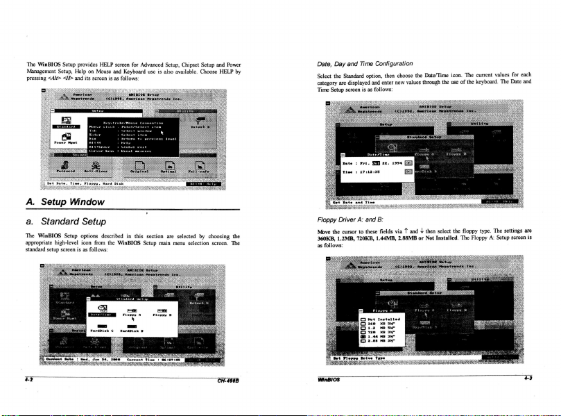
The
WinBIOS
Management
pressing
A.
Setup
a.
Standard
The
WinBIOS
appropriate
standard
setup
4-2
Setup,
<4/t>
high-level
Setup
<H>
Setup
screen
provides
Help
on
and
its
Window
Setup
options
icon
is
as
HELP
screen
Mouse
and
Keyboard
screen
is
as
follows:
Keystrake/Mouse
P
>
Return
described
in
from
the
WinBIOS
follows:
Sr
ate
Flovey
=
==
Harddisk C HardDisk
for
this
Advanced
use
Convention
t
to
previous
section
Setup
a
B
is
main
Setup,
also
level
are
Chipset
available.
selected
menu
selection
Setup
Choose
by
choosing
and
HELP
screen.
CH-496B
Power
the
The
Date,
Day
and
Time
by
Select
category
Time
Setup
the
Floppy
Move
the
360KB,
as
follows:
winBios
Standard
option,
are
displayed
screen
is
:
Fei,
3
17:12:35
Driver
A:
and
cursor
to
these
1.2MB, 720KB,
Configuration
then
and
enter
as
follows:
EJ
22.
B:
fields
1.44MB,
34"
3%"
34"
34"
choose
the
new
values
1994
Eg
via T and \ then
2.88MB
or
Date/Time
through
select
Not
Installed.
icon.
The
current
values
for
type.
each
The
Date
and
The
settings
are
A:
Setup
screen
is
the
use
of
the
keyboard.
the
floppy
The
Floppy
4-3
Page 10
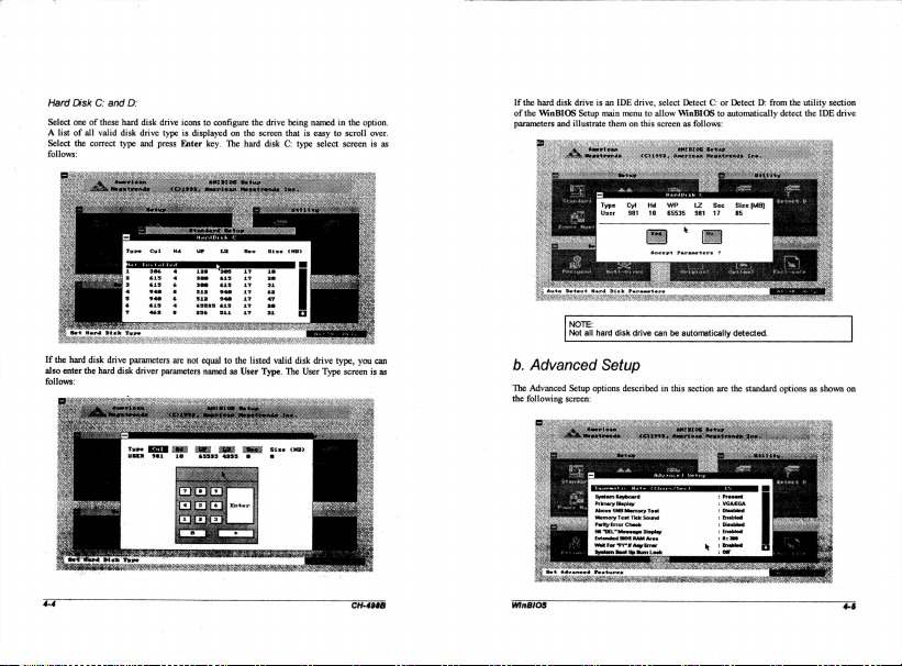
Hard
Disk
Select
A
list
Select
follows:
If
the
hard
also
enter
‘alloows:
one
of
the
of
all
correct
disk
the
C:
these
valid
hard
and
drive
D:
hard
disk
type
parameters
disk
driver
Ture
USER
disk
drive
and
(EME
drive
type
press
are
parameters
(a:
981
16
icons
is
Enter
to
displayed
<RAREIE:
cate
HardDaisk
not
equal
named
mes
65535
configure
key.
Sa
to
4355
If
the
hard
disk
drive
is
an
IDE
drive,
select
Detect
C:
or
Detect
D:
from
the
utility
of the
WinBIOS
Setup
main
menu
to
allow
WinBIOS
to
the
drive
being
named
in
the
on
the
screen
that
The
hard
disk
C:
is
C
the
listed
valid
disk
as
User
Type.
The
SE
size
<u>
@
e
type
is
User
easy
select
drive
Type
to
type,
scroll
screen
screen
option.
you
over.
is
can
is
as
as
parameters
b.
Advanced
The
Advanced
the
following
and
illustrate
NOTE:
Not
Setup
screen:
all
them
Type
User
hard
Setup
options
on
ae
Cyt
981
disk
drive
described
this
Hd
screen
10
Accept
can
in
as
Sep
Pte
‘WP
65535
k
Parameters
be
automatically
this
follows:
as
Lae
LZ
981
section
automatically
Sec _ Size
17
85
7
detected.
are
the
(MB)
standard
detect
$
RAEAEE
options
section
the
IDE
drive
as
shown
on
4-4
CH-498B
WinBios
4-6
Page 11
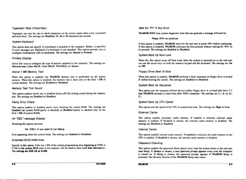
Typematic
Typematic
and
held
System
This
option
if
error
messages
configure
Primary
Select
this
Monochrome,
Above 1 MB
When
this
memory.
system
memory.
Memory
This
option
test.
The
Parity
Error
This
option
Enabled
first 1 MB
Hit
"DEL"
Disabling
from
appearing
Extended
Specify i in
0:300
in
The
settings
£6
Rate
rate
sets
down.
The
Keyboard
does
not
workstations
Display
icon
to
Color
Memory
option
When
this
The
Test
Tick
enables
settings
are
Check
enables
(all
system
of
system
message
this
option
Hit
<DEL>
when
BIOS
this
option
the
system
are‘DOS
(Chars/Sec)
the
rate
settings
specify
are
displayed
with
configure
40x25,
Test
is
enabled,
option
settings
Sound
(turns
Enabled
or
disables
RAM
RAM).
Display
prevents
if
the
system
RAM
Area
if
the
BIOS
1K
or
at
which
are
Disabled,
if a keyboard
if a keyboard
no
keyboards.
the
type
Color
the
is
disabled,
are
Enabled
on)
or
disabled
or
Disabled.
parity
parity
you
want
boots.
top 1 KB
area
in
0:300.
characters
of
80x25,
WinBIOS
is
checked)
to
The
of
low
memory
15,
monitor
VGA/EGA,
the
or
error
run
the
20
is
attached
is
The
settings
memory
memory
Disabled.
(turns
checking
or
Setup
settings
system
will
on
the
or
30
to
not
attached.
attached
or
test
off)
the
Disabled
are
programming
be
used
screen
repeat
characters
the
computer.
are
Absent
to
the
Absent.
test
is
is
done
ticking
for
system
(parity
Enabled
to
store
when a key
per
second.
This
option
or
Present.
computer.
performed
only
on
sound
RAM.
is
checked
or
Disabled.
area
beginning
hard
Rather,
permits
The
the
during
The
disk
is
pressed
it
specifies
you
settings
on
all
system
first 1 MB
the
memory
settings
only
at
639K
information.
CH-498B
Wait
for
"F1"
If
Any
POST
option
option
The
Boot
this
the
arrow
Drive
option
booting
Boot
sets
Boot
sets
Cache
is
enabled.
are
Disabled
Cache
enabled
enabled.
enables
If
on.
See
runs
Press
is
enabled,
is
disabled,
settings
Up
option
Seek
is
the
Up
the
attempts
Up
the
enables
If
Checking
Always
If
Setup
Security
system
<F1>
Num
turns
keys
At
enabled,
system.
Sequence
sequence
CPU
speed
secondary
If
or
internal
disabled
the
is
Section
Error
diagnostic
to
continue
WinBIOS
WinBIOS
are
Enabled
Lock
off
Num
on
both
the
Boot
WinBIOS
The
of
boot
to
boot
from
Speed
of
the
CPU
Disabled
Enabled.
cache
is
chosen,
password
chosen, a user
is
chosen,
of
tests
waits
continues
or
Lock
numeric
performs a Seek
settings
drivers
after
at
cache
is
chosen,
memory.
the
check
option
the
the
WinBIOS
that
for the
the
Disabled.
when
keypad
are
Enabled
(either
POST
system
memory.
the
If
enabled
internal
password
password
can
generate a message
end
user
boot
process
the
system
and
the
command
or
floppy
completes.
boot
time.
If
enabled
external
is
cache
memory
lee
time
prompt
prompt
Setup
main
to
press
without
is
powered
keyboard.
Disabled.
drive
The
The
settings
is
cache
selected,
the
system
appears
appears
menu.
<F1>
on
floppy
A:
or
settings
selected,
memory
the
cache
is
disabled.
boots
every
if
followed
before
waiting
on
so
The
settings
hard
are
are
High
external
is
or
time
WinBIOS
by:
continuing.
for
the
end
drive
A:or/and
disk
drive
C:,
A:
or
disabled.
memory
the
end
the
computer
Setup
<F1>
are
Low.
or
cache
in
user
A:,
The
user
47
to
On
C:)
the
is
WinBIOS
If
this
If
this
be
to
are
of
are
on
the
or
pressed.
System
When
can
use
or
Off.
Floppy
When
B:
before
System
This
option
=
WinBIOS
System
This
option
External
This
memory
settings
Internal
This
option
CPU
is
Password
This
option
runs
Setup.
is
tumed
executed.
WinBios
On,
this
option
Page 12
Video
Shadow
Video
Shadow
When
this
(shadowed)
ShadowCs800,
ShadowCCoo,
ShadowD000,
ShadowD400,
ShadowD800,
ShadowDCo0,
ShadowE000,
These
options
The
settings
Main
BIOS
When
this
copied
(shadowed)
IDE
Block
The
BIOS
that
specifies
present.
The
IDE
LBA
When
set
otherwise
IDE
32
Bit
If
the
IDE
enable
to
should
be
Video
Shadow
When
set
normal
speed.
option
to
RAM
enable
are
Shadow
option
Mode
support
the
setting
Mode
to
enable,
the
IDE
Mode
hard
disk
speed
disabled.
to
enable,
C000,
C400,
is
set
for
16K
16K
16K
16K
16K
16K
64K
Disabled
is
set
to
the
maximum
are
the
hard
drive
up
the
Before
the
16K
16K
to
Enabled,
faster
shadowing
or
F000,
to
enabled,
RAM
for
transfer
number
Disabled
BIOS
disk
drive
and
IDE
Video
system
execution.
of
Enabled.
64K
faster
of
multiple
or
can
support
size
IDE
access
Init
power
the
video
The
the
contents
the
main
execution.
of
sectors
Enabled.
the
limitation
controller
speed.
It
on
is
ROM
settings
of
BIOS
The
sectors
that
IDE
is
card
does
initiated
area
are
the
ROM
setting
to
can
hard
528
support
not
to
from
Disabled
ROM
area
are
and
from
be
transferred
disk
drive
MB.
32-bit
support
fast
C0000h - C7FFFh
or
Enabled.
area
named
from
F0000h - FFFFFh
Disabled
an
IDE
at a time
size
bigger
transfer,
32-bit
transfer,
speed,
otherwise
in
the
or
drive.
you
is
option
Enabled.
This
may
than
can
this
it
is
copied
option
also
528
set
feature
only
title.
is
be
MB,
it
to
in
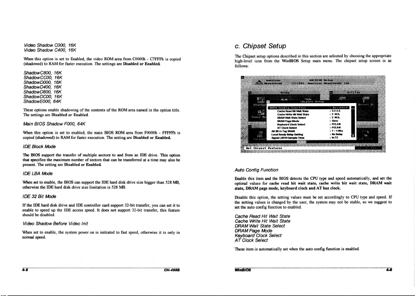
c.
Chipset
The
Chipset
high-level
follows:
Auto
Config
Enable
this
optimal
state,
DRAM
Disable
the
setting
set
the
auto
Cache
Cache
DRAM
DRAM
Keyboard
AT
Clock
These
item
setup
icon
item
values
page
this
option,
values
config
Read
Write
Wait
Page
Clock
Select
is
automatically
Setup
options
from
Function
and
for
cache
mode,
is
function
Hit
Wait
Hit
Wait
State
Mode
Select
the
the
the
changed
Select
described
WinBIOS
BIOS
read
keyboard
setting
by
to
enabled.
State
State
set
detects
hit
values
the
when
in
wait
clock
user,
the
this
Setup
the
must
state,
and
auto
section
main
CPU
AT
be
the
system
config
are
menu.
type
cache
bus
set
accordingly
function
selected
The
and
speed
write
clock.
may
not
by
choosing
chipset
setup
automatically,
hit
wait
state,
to
CPU
be
stable,
is
enabled.
type
so
the
appropriate
screen
and
DRAM
and
we
suggest
set
speed.
is
wait
as
the
If
to
4-8
CH-4988
WinBIiOs
4-9
Page 13
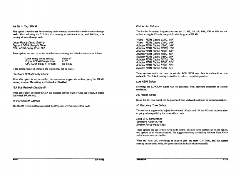
Alt
Bit
This
option
mode.
running
Local
Signal
CPU
These
If
the
Hardware
When
memory
ISA
Bus
When
the
refresh
DRAM
The
DRAM
in
Tag
is
When
at
write-through
Ready
LDEV#
ADS#
options
Local
Signal
CPU
setting
DRAM
this
option
module.
Refresh
set
to
slow,
DRAM
Refresh
refresh
SRAM
used
to
selecting
Delay
Sample
Delay
are
used
ready
ADS#
values
is
The
it
only.
Method
method
set
the
mode.
Setting
IT
or
to
LDEV#
is
changed,
Parity
set
to
setting
Disable
enable
the
7+1
Time
Not
set
delay
Sample
delay
Check
enabled,
the
can
secondary
bits,
the
local
setting:
1T
or
the
are
Enabled
Bit
ISA
select
it
bus
time:
Not:
system
the
bus
the
cache
is
running
access
may
system
or
Disabled.
standard
RAS
memory
timing,
Delay
in
No
not
can
refresh
only
in
at
write-back
T2
delay
be
stable.
support
or
CAS
write-back
the
default
IT
the
cycle
or
before
mode
mode,
values
without
when
RAS
and
set
mode.
or
are
parity
to
write-through
8+0
bits,
it
as
follows:
bit
DRAM
fast,
it
enable
Divider
for
Refresh
The
divider
for
refresh
frequency
options
are
1/1,
1/2, 1/4, 1/8,
1/16,
1/32
or
1/64
and
cacheable
chipset
card
can
software
and
or
emulation.
recovery
be
one
flash
the
the
or
non
chipset
time
option,
80486
system
is
default
setting
Video
ROM
Video
ROM
Adaptor
ROM
Adaptor
ROM
Adaptor
ROM
AdaptorROM
AdaptorROM
Adaptor
ROM
AdaptorROM
Adaptor
ROM
System
ROM
These
options
cacheable.
The
Low
A20#
Selecting
the
emulation.
RC
Reset
Select
the
RC
10
Recovery
This
option
to
get
good
Hold
CPU
Software
Enable
Force
These
options
two
options
and
other
options
When
the
Hold
running
in
non-turbo
is
1/1
to
Cache
Cache
Cache
Cache
Cache
Cache
Cache
Cache
Cache
Cache
Cache
which
default
Select
LOWA20#
Select
reset
signal
Time
Select
is
supported
compatibility
percentage
Flash
80486
Read
are
use
for
or
all
options
are
disabled.
CPU
mode,
be
compatible
Coo0,
C400,
C800,
CCO00,
D000,
D400,
D800, 16K
DCOO,
E000,
E800,
F000,
are
used
setting
is
signal
will
be
to
adjust
for
some
Miss
non-turbo
enabled.
percentage
the
16K
16K
16K
16K
16K
16K
16K
32K
32K
64K
to
set
disabled
will
generated
the
add-on
mode
The
is
green
with
the
the
to
be
generated
from
on
board
cards.
control.
suggested
enabled
function
general
ROM
reduce
I/O
(any one
is
DRAM.
BIOS
compatible
from
keyboard
port
The
non-turbo
setting
disabled
area
data
problem.
keyboard
controller
and
ISA
bus
control
is
enabling
from
1/16~7/16),
automatically.
is
controller
or
I/O
410
CH-498B
WinBios
4-99
Page 14
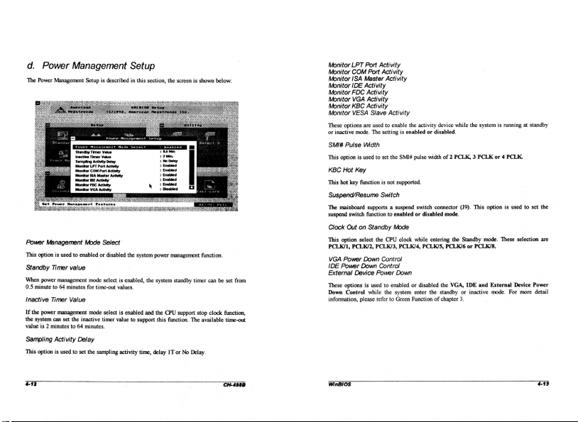
d.
The
Power
Power
This
option
Standby
When
0.5
minute
Inactive
If
the
the
system
value
Sampling
This
option
Power
Management
Management
is
used
Timer
power
management
to
64
Timer
power
management
can
is 2 minutes
Activity
is
used
Management
Setup
Mode
to
enabled
value
mode
minutes
for
Value
mode
set
the
inactive
to
64
minutes.
Delay
to
set
the
is
described
Select
or
disabled
select
time-out
select
timer value
sampling
the
is
enabled,
values.
is
enabled
activity
Setup
in
this
system
to
support
time,
section,
power
the
system
and
the
delay
this
CPU
the
screen
management
standby
support
function.
1T
or
No
is
timer
stop
The
Delay.
shown
function.
can
clock
available
below:
be
set
from
function,
time-out
Monitor
LPT
Monitor
COM
Monitor
ISA
Monitor
IDE
Monitor
FDC
Monitor
VGA
Monitor
KBC
Monitor
VESA
These
options
or
inactive
mode.
SMI#
Pulse
This
option
is
KBC
Hot
Key
This
hot
key
Suspend/Resume
The
mainboard
suspend
switch
Clock
Out
This
option
PCLK/1,
PCLK/2,
VGA
Power
IDE
Power
External
Device
These
options
Down
Control
information,
Port
Activity
Port
Activity
Master
Activity
Activity
Activity
Activity
Activity
Slave
are
used
to
The
setting
Wath
used
to
set
function
is
not
Switch
supports a suspend
function
to
on
Standby
select
the
CPU
PCLK/3,
Down
Control
Down
Control
Power
is
used
to
while
the
please
refer
Activity
enable
is
the
SMI#
supported.
enabled
Mode
clock while
PCLK/4,
Down
enabled
system
to
Green
the
enabled
pulse
switch
or
or
enter
Function
activity
or
width
disabled
entering
PCLK/5,
disabled
the
device
while
disabled.
of 2 PCLK, 3 PCLK
connector
(J9).
mode.
the
Standby
PCLK/6
the
VGA,
standby
or
of
chapter
3.
the
This
or
PCLK/8.
IDE
inactive
system
mode.
and
or 4 PCLK.
option
External
mode.
is
running
These
is
For
used
selection
Device
more
at
to
standby
set
the
are
Power
detail
+7
CH-498B
WinBIOS
4-19
Page 15
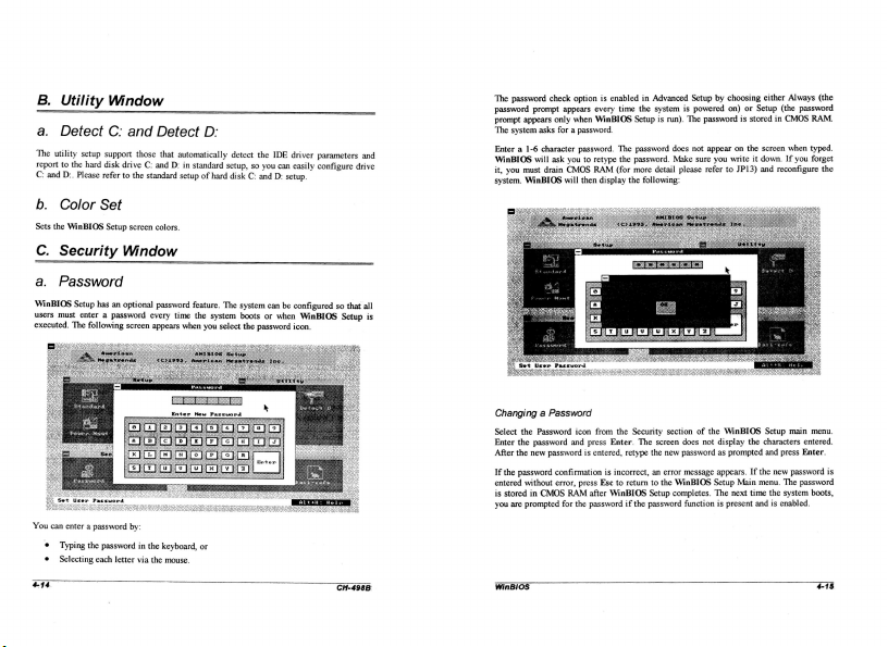
B.
a.
The
utility
report
C:
and
b.
Sets
the
C.
a.
WinBIOS
users
executed.
You
can
e
414
Utility
Detect
setup
to
the
hard
D:.
Please
Color
WinBIOS
Security
Password
Setup
has
must
enter a password
The
following
enter a password
Typing
the
Selecting
each
Window
C:
support
disk
refer
Set
Setup
an
password
letter
and
those
drive
C:
to
the
standard
screen
Window
optional
every
screen
by:
in
the
via
the
Detect
that
and
D:
colors.
password
time
appears
keyboard,
mouse.
D:
automatically
in
standard
setup
of
hard
feature.
the
system
when
you
select
or
setup,
disk
The
detect
system
boots
the
the
so
C:
password
The
password
check
option
is
enabled
in
Advanced
Setup
by
choosing
either
Always
password
prompt
appears
every
time
the
system
is
powered
on)
prompt
appears
only
when
WinBIOS
Setup
is
The
system
asks
for a password.
Enter a 1-6
character
IDE
driver
parameters
WinBIOS
configure
so
Setup
CH-498B
that
and
drive
all
is
you
can
easily
and
D:
setup.
can
be
configured
or
when
icon.
WinBIOS
it,
you
system.
Changing a Password
Select
Enter
After
If
the
entered
is
stored
you
are
WinBIOS
will
must
WinBIOS
the
the
password
the
new
password
without
in
prompted
ask
drain
Password
password
confirmation
error,
CMOS
you
CMOS
will
and
RAM
for the
password.
to
retype
RAM
then
icon
from
press
is
entered,
press
after
password
display
Esc
The
the
(for
the
Enter.
retype
is
incorrect,
to
return
WinBIOS
if
password
password.
more
the
following:
Security
The
the
password
detail
screen
the
an
to
Setup
run).
does
Make
please
section
new
error
the
WinBIOS
completes.
The
not
sure
of
does
password
message
function
password
appear
you
refer
the
WinBIOS
not
display
as
appears.
Setup
The
is
or
is
on
write
to
JP13)
prompted
Main
next
present
stored
the
it
the
If
time
Setup
in
screen
down.
and
Setup
characters
and
the
new
menu.
the
and
is
(the
password
CMOS
RAM.
when
typed.
If
you
forget
reconfigure
main
menu.
entered.
press
Enter.
password
The
password
system
boots,
enabled.
(the
the
is
4-18
Page 16
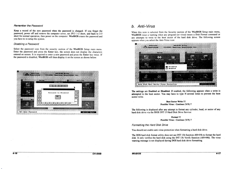
Remember
the
for
have
power
normal
to
re-setup
Password
of
off
operation,
Keep a record
password,
short
you
Disabling a Password
Select
the
password
Enter
the
password
entered
on
screen.
the
password
is
disabled,
the
and
It
new
and
the
icon
is
required
password
remove
then
system.
from
press
WinBIOS
the
the
power
the
to
when
computer
on
the
security
Enter
key,
enter a new
will
then
the
password
cover,
computer.
section
the
password
display
set
of
screen
it
on
is
JP13
WinBIOS
the
WinBIOS
does
and
the
changed.
1-2
not
press
screen
short,
erases
display
the
as
If
Setup
Enter
shown
you
and
the
forget
back
password
main
the
characters
key
below:
to
menu.
twice.
b.
the
2-3
and
Anti-Virus
When
this
WinBIOS
any
attempts
appears
when
icon
is
selected
issue a warning
to
write
you
select
when
to
the
the
from
the
any
boot
Anti-Virus
Security
program
sector
icon:
of
section
(or
virus)
the
of
hard
the
WinBIOS
issues a Disk
disk
drive.
The
Setup
Format
following
main
command
menu,
screen
or
If
ja | ee
as
tectron
G
Disabled
BC
Enabled
4-16
Fassword
is
Disabled
AT
Te
ey
ze
CH-498B
The
settings
attempted
sector
The
following
hard
disk
Formatting
You
should
The
DOS
disk.
It
warming
WinBios
write.
only
message
to
drive
not
hard
are
Enabled
the
boot
is
displayed
via
the
the
Hard
enable
disk
verifies
is
sector.
BIOS
Disk
anti-virus
format
the
not
displayed
or
after
utility
hard
Disabled.
You
may
Boot
Possible
any
INT
13
Possible
Drive
protection
does
disk
using
during
If
enabled,
have
to
Sector
Write
Virus : Continue
attempt
to
Hard
Disk
Format
Virus : Continue
when
not
use
INT
the
INT
DOS
hard
the
following
type N several
!!!
(Y/N)
format
any
Drive
Service:
!!!
(Y/N)
formatting a hard
13h
function
13h
Verify
disk
drive
appears
times
?
cylinder,
?
AH=05h
function
formatting.
to
head,
disk
(AH=04h).
when a write
prevent
or
sector
drive.
to
format
is
the
boot
of
any
the
hard
The
virus
4-17
Page 17
If
the
anti-virus
attempt
to
format
If
you
select
Continue,
If
you
do
not
(depending
on
example,
does
D.
Default
The
icons
in
this
options.
Not
only
you
an
choose a group
having
configuration-related
Original
Choose
the
Original
Setup
when
you
Optimal
You
can
load
Optimal
icon.
system
performance.
automatically.
Fail-Safe
You
can
load
from
the
Default
The
Fail-Safe
stable
settings.
feature
the
want
how
at
least
section
can
first
the
optimal
The
the
Fail-Safe
section
settings
Use
is
hard
formatting
to
many
five
Window
you
of
icon
began
Optimal
If
of
provide
this
option
enabled, a virus
disk
drive.
proceeds
continue
formatting,
retries
are
entries
before
permit
you
use
these
settings
that
problems.
to
return
to
this
WinBIOS
default
settings
default
CMOS
RAM
WinBIOS
the
WinBIOS
far
from
as a diagnostic
warning message
as
performed
the
Format
to
select a group
icons
to
quickly
have a better
the
system
Setup
for
the
settings
is
corrupted,
Setup
option
Setup
optimal
aid
normal.
you
may
by
the
utility
set
chance
configuration
session.
WinBIOS
are
best-case
settings
main
menu.
system
if
the
have
upper-level
is
actually
of
settings
system
of
Setup
values
the
Optimal
by
performance,
system
will
be
displayed
to
press N several
software).
aborted.
for
all
configuration
working
when
values
present
options
that
settings
selecting
the
but
is
behaving
when
DOS,
WinBIOS
parameters,
the
system
in
WinBIOS
by
selecting
should
optimize
are
Fail-Safe
are
the
erratically.
times
Setup
loaded
icon
most
you
for
is
the
E.
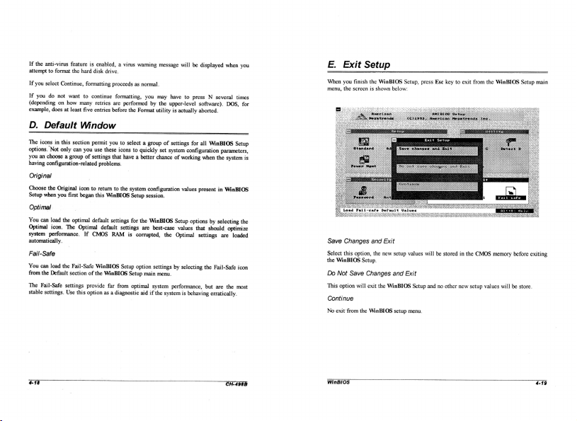
When
menu,
Save
Select
the
Do
This
Exit
you
the
Changes
this
WinBIOS
Not
option
finish
screen
option,
Save
will
Setup
the
is
and
the
Setup.
Changes
exit
WinBIOS
shown
Exit
new
the
below:
setup
and
WinBIOS
Setup,
values
Exit
Setup
press
will
Esc
key
to
exit
from
the
WinBIOS
Setup
main
be
stored
in
the
CMOS
memory
before
exiting
and
no
other
new
setup
values
will
be
store.
Continue
No
exit
from
the
WinBIOS
setup
menu.
4-18
CH-498B
WinBIOS
4-19
Page 18
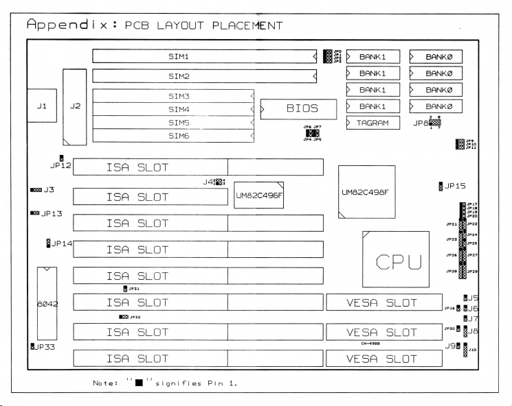
Appendi
J4
P|
maa
J 3
HB
P13
Hpis
BUPSS
RK
J2
|
|
|
|
|
}
fL
x?
|
ISA
Isa
ISA
ISA
ISA
ISA
ISA
ISA
Note:
PCB
Bors
ED
sp32
|'MB
LAYOUT
SIM1
arene
SLOT
SLOT
SLOT
SLOT
SLOT
SLOT
SLOT
SLOT
signifies
PLACEMENT
|
Jails
|
UMB2C496F
N
|
| |
|
|
|
|
Pin
1.
q
Ee } BANKi | >
q
b
BaANK1 | pb
b
BANK1 | >
=
|
UM82C498F
IN
|
a
BaNKi | >
7
BIOS
—— b tacRaM | JPeia
mG
apy
|
|i
|
|
vesA
ovesa
VESA@
SLOT
stot
SLOT
|
BANKo
BANKo
BANK
BANKo
RUP15
|g
[8
198
|
|
|
|
|
EE:
fd
BU7
ihe
Fo
 Loading...