

Page 1
CH-486-33A
User’s
Manual
Page 2

1st Edition, June 1991
The information contained in this manual is
subject to change without notice
__ _ _
_.___ ____________
IBM
PC/XT/AT/PS-2
are registered trademarks of
International Business Machines Corporation.
AMI
is a trademark of American Megatrends, inc.
486 is a trademark of Intel Corporation.
Other brand and product name or trademarks
and/or registered trademarks of respective companies.
Page 3
Table Of Contents
1. Introduction
2.
Hardware Description
I
System Description
21
22-Connector and Jumper Settings
I
DRAM Bank Configuration
23
-
SRAM Configuration
24
3
BIOS Setup
-
BIOS Overview
31
I
Standard CMOS Setup
32
-
Advanced CMOS Setup
33
-
Advanced
34
I
Auto Configuration with BIOS
35
Defaults.
Auto Configuration with Power-On
3-6
Defaults
’
1
-
Write To CMOS and Exit
37
-
I
I
Do
38
Not Write To CMOS and Exit
Chipset
Setup
Page 4
1
htroduction
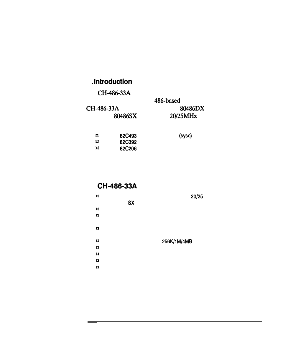
The
CH-486.33A
performance for high-end
CH-486.33A
or INTEL
is a three-chip solution offering optional
486.based
is designed for INTEL
80486SX
running for
AT systems. The
80486DX
20/25MHz
combines three
running 33 MHz
major functions:
x
The
82C493
If
The
tl
The
System Controller
82C392
Data Buffer Contrdler (DBC)
82C206
Integrated Peripheral Controller (IPC)
(sysc)
l-l. CH-486-33A Mainboard Specification
33 MHz INTEL 80486 DX CPU OR
80486 SX CPU
ISA architecture
Copy-Back Direct-Mapped Cache with size of 64KB
or 256 KB selectable
II
Up to 32 MB of local high-speed page-mode DRAM
memory space
DRAM TYPE support 256K/i
Control of two non-cacheable regions
Shadow
Optional Cacheable of shadow video BIOS
Turbo/slow speed selectable for hardware and
software controller
RAM support
M/4MB
20125
MHz INTEL
Introduction
1-1
Page 5
WEITEK 4167 coprocessor socket on board
On board rechargeable battery back-up for CMOS
configuration and real-time dock
Optimized for
OS/2,
window/386, window 3.0, XENIX,
UNIX software operation
Baby AT size, with XT/AT mounting
hole
l-2
lntroductlon
Page 6
2. Hardware Description
2-l
System Description
80486
Microprocessor
The 80486 is a high performance
on-chip memory management, floating point and cache
memory units. It is binary compatible with members of the 86
architectural family. The 486 CPU contains all the features of
the 386 CPU with enhancements to increase performance.
On-chip Floating Point Control Unit
The operation of the 486 microprocessor’s on-chip floating
point control unit is exactly the same as the 387 math
coprocessor. Software written for the 387 math coprocessor will
run on the on-chip floating point unit without any
modification. It occupies
8OOOOOFOH-SOOOOOFFH
I/O
and operates in parallel with the
arithmetic and logic unit and provides arithmetic instructions
for a variety of numeric data types.
On-chip Cache Memory
32.bit
microprocessor with
address range of
The
8KB
on-chip cache is a 4-way set associative write-through
code and data cache memory. Individual pages can be
designated as cacheable or non-cacheable by software or
hardware. The cache can also be enabled and disabled by
software or hardware.
Hardware Description
Page 7
4167 Floating-point Coprocessor
The WEITEK 4167 is a high-performance single-chip
floating-point coprocessor for 80486 microprocessor. It is
upwardly binary compatible with the WEITEK 3167
coprocessor.
The 4167 coprocessor is a memory-mapped peripheral
communicates with the
connects the main memory to CPU. The
respond to memory addresses
CIFFFFFFH. Writing to this ;ddrcss space will
to execute this
fractions
coprocessor to drive the
80486
over the
COOOOOOO1:
same address bus tklt
coprocessor
i
through
will
cause the
and reading from it will cause the
data
bus.
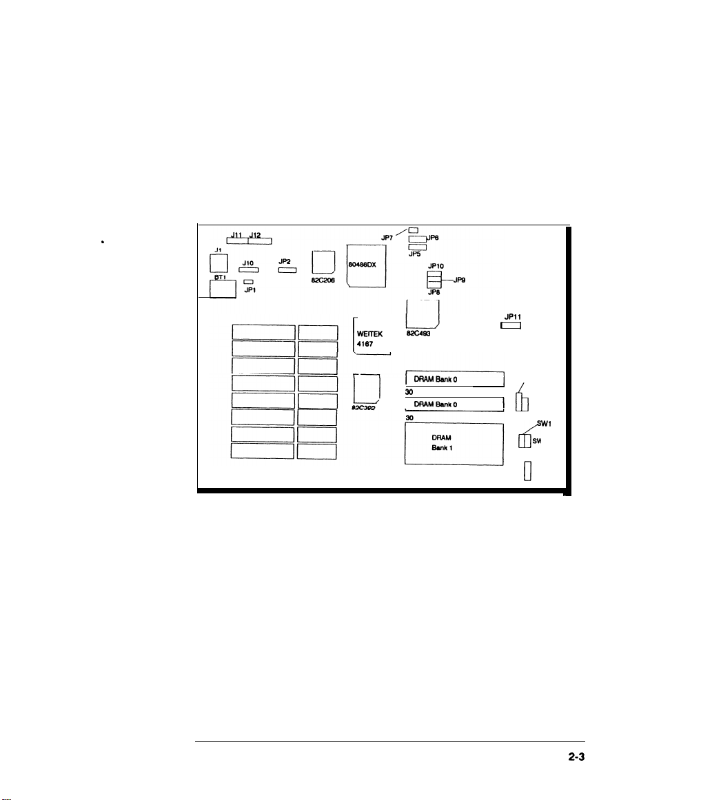
2-2 Connector and Jumper Settings
This chapter describes the
CH-486.33A main bo;rrd’s
jumpers
and connectors
The system layout are shown on the next
purge.
that
4
107
Hardware Description
Page 8
.
JPll
I
WEITEK
4167
1
82c4w
1
DRAMBank
30
DRAMBank
I
J23
324
I
il
Wl
SW2
d
JP12
0
Hardware Description
2-3
Page 9

SW1
Hardware Reset switch Connector
:
sw2:
.
.
Jl
JlO:
Jll
,
J23:
J24:
JP12:
Hardware Turbo Switch Connector
Keyboard Connector
External Battery Connector
J12: Power Connector
Keylock and Power LED Connector
Speaker Connector
Turbo LED Connector
2-4
Hardware Description
Page 10
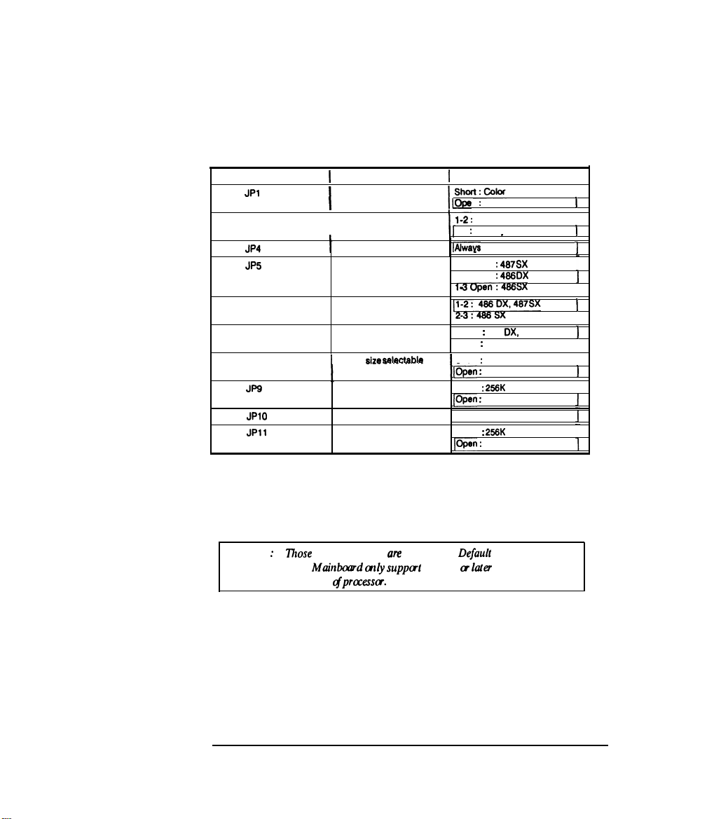
Jumper
JPl
JP2
JP4
JPS
JP6
1
Description
Monitor Type Selectable
I
CMOS power
I
CPU selectable
CPU selectable
1
Setting
n : Monochrome
1-2
:
Clear CMOS RAM
2-3 : Backup CMOS RAM
I
[Always
1
1-2:
(2-3
13Upen:4BSX
_
.
2-3 Short
-
487SX
:
4860X
I
1
I
1
I
JP7
JP8
Jp9
JPlO
JPll
NOTE : 1.
TItose
2. This
stepping
CPU selectable
1
Cache
$i28 Sdetctabl8
Cache size selectable
Cache size selectable
enclosed in box
Mainbmud
mly supput Intel C u
cfpracesscx.
_-.--_-.-.-
ate
Mainboard
[Short : 486
Open : 486 SX
Short : 256K
@pen
Short :
IOpen
[Always Open
Short :
IOpen
:
64K
:
64K
:
64K
256K
256K
OX,
487SX
Default
Iater
J
Hardware Description
2-5
Page 11
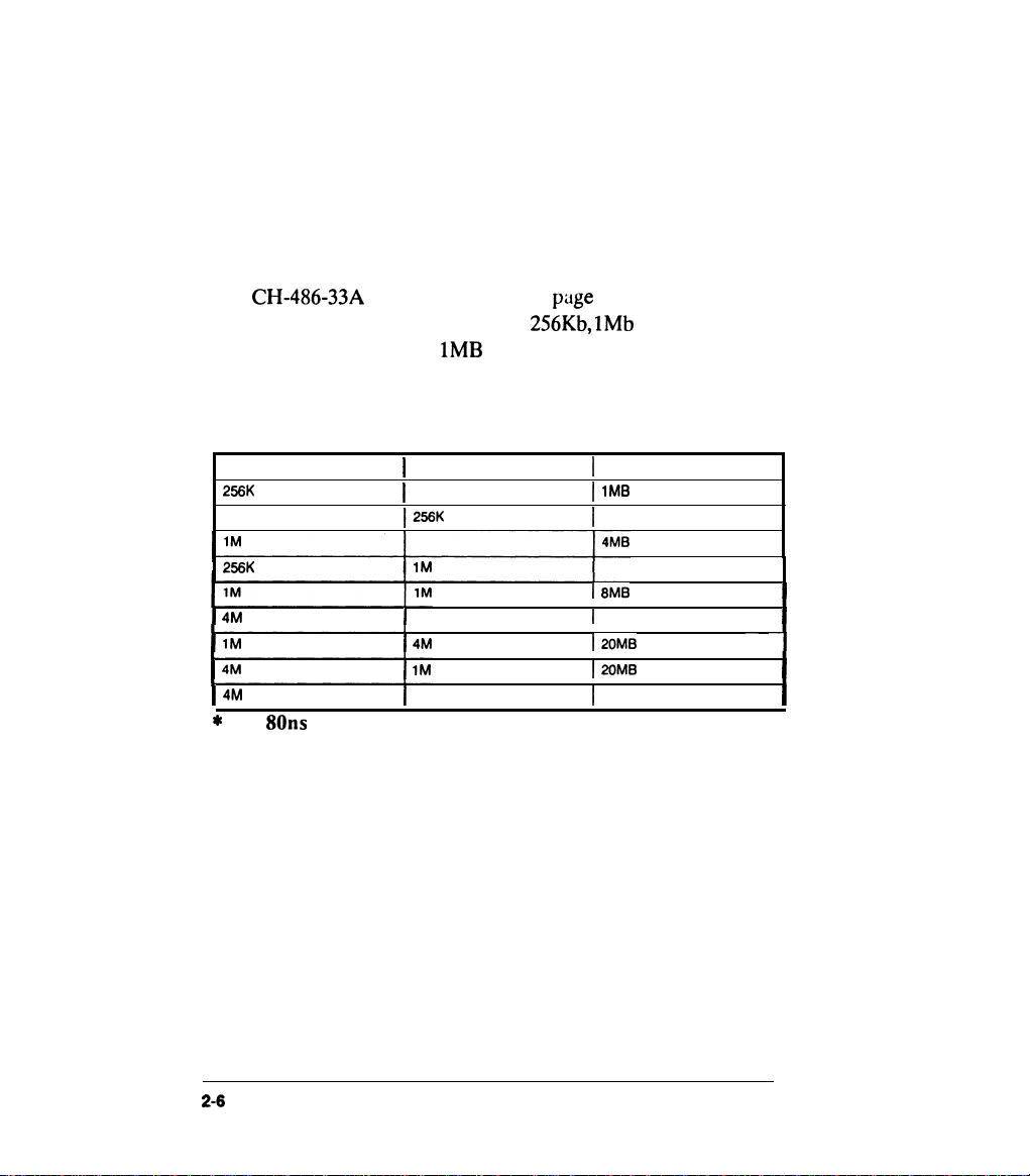
2-3. DRAM Bank Configuration
The
CH-486.33A
memory, DRAM devices are either
Total memory is between
illustrates the configuration supported.
supports 2 banks of
256Kb, 1Mb
1MB
and 32MB. The following table
page
mode local
or 4Mb large.
Bank 0
256K
256K
256K
1 4M
I
lfvl
I
4M
I
4M
*
Use 80ns DRAM
1
Bank 1
I
I256K
1M
I
I
4M
I
lM
4M
I
1
Total
1MB
I
1
2MB
5MB
i8MB
1
16MB
I20MB
I2OMB
1
32MB
I
I
- -1
I
I
2-6
Hardware Description
Page 12
2-4
SRAM Configuration
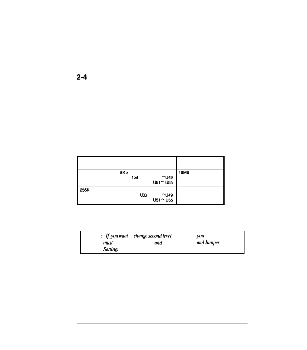
The CH-486-33A has a non-pipeline mode with a 16 bytes line
size copy-back Direct-mapped cache, because this cache
controller design two-way interleave cache read/write, so only
support 64K or 256K secondary cache size.
The following table shows the TAG RAM size, cache RAM size
and cacheable main memory size supported by CH-486-33A.
Cache size (KB)
64K
256K
Note : . If
TAG RAM size
8Kx 8bit U34
64K x lbit U33
32K x 8bit U34 32K x 8bit 32MB
64K x 1 bit
you
waut
mrst
change the SRA M
Setthg.
Hardware Description
to
U33
charge
Cache Cacheable main
RAM size memory
8K x 8bit
u47 “U49
us1 - us5
u47 “U49
us1 - us5
secortd
arid
16MB
Ier~el
cache size,
TAG RAM size
you
aud Jutqw
2-7
Page 13
3-l.
BIOS OVERVIEW
3.BlOS
SETUP
The SETUP program is used to configure the system. These
system options are stored in the CMOS. If the CMOS is good,
the system is configured with the values stored in the CMOS. If
the CMOS is bad, the system is configured with the default
values stored in the ROM file.
There are two (2) sets of BIOS values stored in the ROM file
tl
The BIOS Setup default values
n
The Power-On default values
:
The BIOS Setup default values are the default values which are
supposed to give optimum performance for the system. They
are the best case default values.
The Power-On default values are the default values for the
table values for the system. They are the worst case default
values.
BIOS SETUP
3-l
Page 14

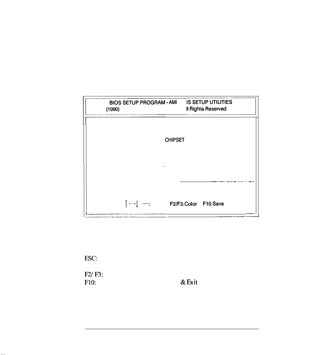
There are two ways to enter the BIOS setup program
1. Whenever BIOS detects any equipment error or the CMOS
contents are not consistent with the equipment.
2. After the power on memory test, the screen will show:
Hit
<DEL>
Press the DEL key to get the following screen:
If you want to run setup
3-2
BIOS
SETUP
Page 15
-
AMI
BIOS SETUP UTILITIES
(1990)
American Megatrends Inc., All
Rights
--I
Reserved
STANDARD CMOS SETUP
ADVANCED CMOS SETUP
ADVANCED
CHIPSET
SETUP
AUTO CONFIGURATION WITH BIOS DEFAULTS
AUTO CONFIGURATION WITH POWER-ON DEFAULTS
WRITE TO CMOS AND EXIT
DO NOT WRITE TO CMOS AND EXIT
.
__ _______
___.__ ___ --
Standard CMOS Setup for changing Time, Date, Hard Disk Type, etc.
_~___
L
~~____
ESC:Exit
_.__._ _______ _ ___~_
I- 1
-
____~__
l
-- :
Sel
F2/F3:Color
FlO:Save
---___-
& Exit
_-
Explanation of keys:
FCC:
Arrow keys:
F2/ F3:
FlO:
BIOS SETUP
Exit to setup program
Cursor movement
Change Color
Save Setup values &
&it
to setup program
3-3
Page 16
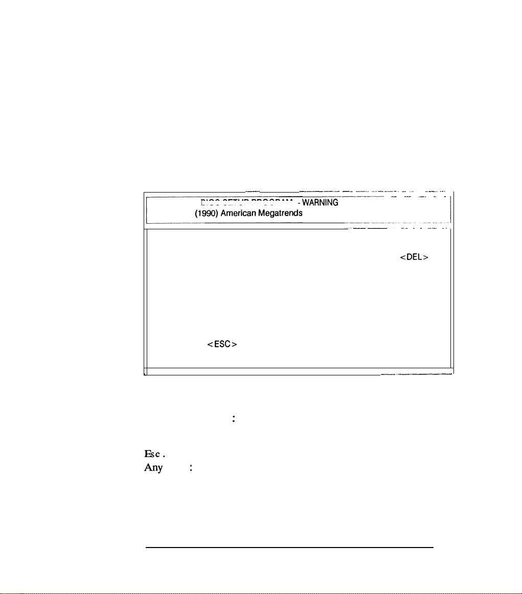
The user is given a warning message before he is allowed to
change any of the setup parameters. The warning message is
shown as following:
--
BIOS SETUP PROGRAM
Improper Use of Setup may Cause Problems !!
If System Hangs, Reboot System and Enter Setup by pressing the <
Do any of the following After Entering Setup
(i)
Alter options to make system work
(ii) Load BIOS Setup Defaults
(iii) Load Power-On Defaults
Hit <
ESC>
to stop now, Any other key to Continue
Figure 3 : BIOS Setup Warning Message
Explanation of keys:
.
ESC
Any*
Exit to previous screen
keys : Continue choose setup program
______- -- --__ _.._-____--_
______________
-WARNING
Inc., All Rights Reserved
INFORMATION
-_ .----.- .-.
__
___
.-- __
-_
. _ -_
DEL >
key
-
_.
3-4 BIOS SETUP
Page 17

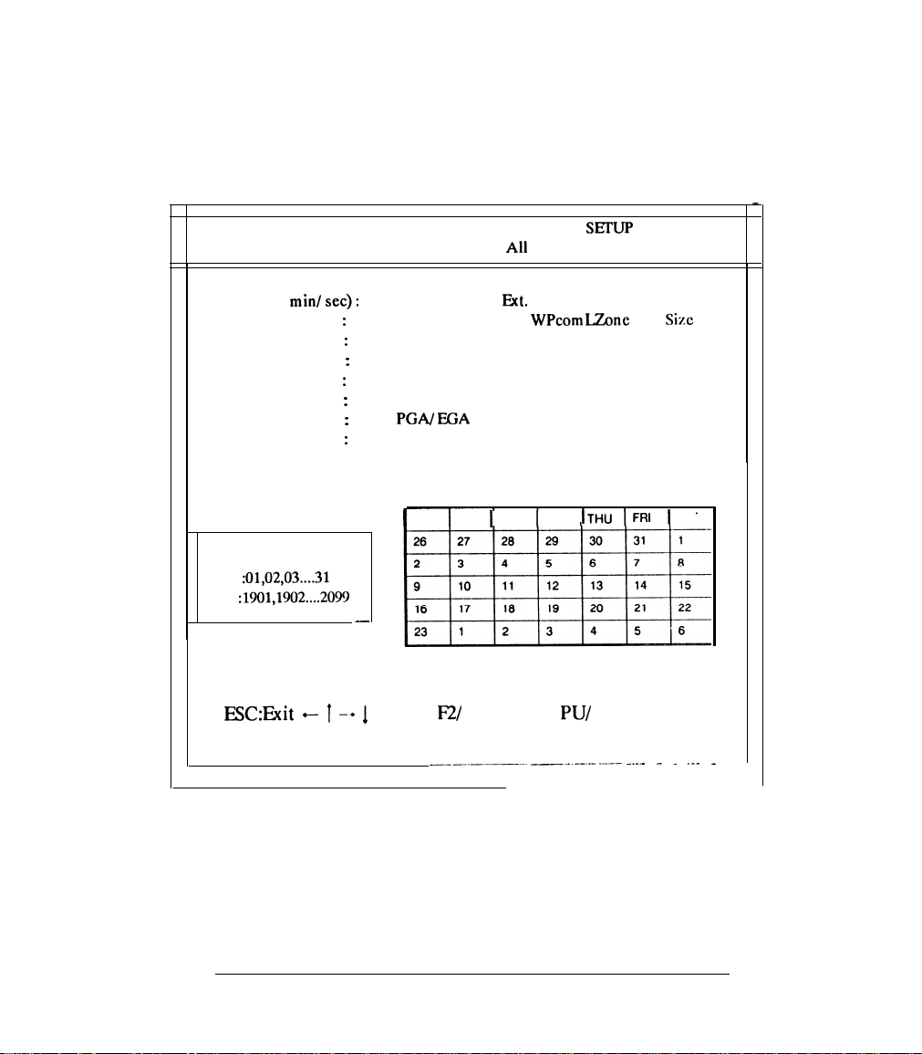
3-2 STANDARD CMOS SETUP
This option is used to configure the following options:
Date: Month, Date and Year
Time: Hour, Minute and Second
Daylight Saving: Disabled or Enabled
Hard Disk C: and Hard Disk D: The user can choose
any of the standard hard disk types from 1 to 46 or he
can choose type 47 which is the user defineable type.
The user must enter the hard disk parameters if he
wants to choose the user-definable hard disk type
per drive, i.e., type 47 may be different for drive C: and
for drive D:.
Floppy drive A: and Floppy drive B: 360KB 5.25,
1.2MB 5.25,
Primary Display: Monochrome, Color 40 x 25,
VGA/PGA/EGA,
Keyboard: Installed or Not Installed
720KB
3.5”, 1.44MB 3.5”,
Color 80x25, Not Installed
Not Installed
BIOS SETUP
3-5
Page 18
BIOS SETUP PROGRAM-STANDARD CMOS
(C)1990 American Megatrends Inc., All Rights Reserved
SEI’UP
-
Date (mm/ date/ year): Wed, Jun 05 1991
lime (hour/ min/
Daylight saving
Hard disk C: type: Not Installed
Hard disk D: type
Floppy drive A
Floppy drive B
Primary display
Key board
Month:Jan,Feb,....Dec
Date
:01,02,03....31
Year
:1901,1902....2099
ESC:Exit -
set):
15 : 35 : 50
:
Disabled
:
Not Installed
:
1.2 MB, 5.25”
:
Not Installed
:
VGA/ PGA/ FGA
:
Installed
.-
--• 1
Select
1
1
SUN1 MON 1 TUE
F2/
___________. _-_.-.--._- -.---
Base memory: 640 KB
Ext.
memory: 7168 KB
Cyln Head
WPcom
1
WED 1
F3: Color
LZone Sect Size
THU
PU/
PD:Modify
-__- - _ .-- -
1
SAT
3-6
BIOS SETUP
Page 19
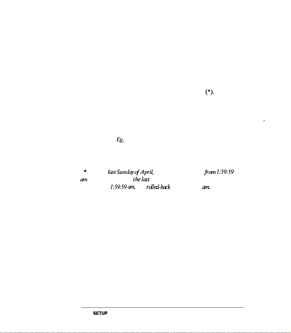
Note: Daylight Saving
The RTC has a built-in capability to automatically adjust the
time on the two daylight savings days of the year
(*).
If this is
desired, set the field to “Enable”.
Otherwise, set field to “Disabled”. Note that in general, nothing
will be immediately observable by setting the field to either
state.
.
*
On the
am
to 3:00:00 am On
first reaches
lcrrt
Sun&y
1:59:59 am,
Daylight Savings..
Eg,
Daylight Savings..
@April”
thelast
Sunday in October, when the time
it is
rdled-barck
......
Enable
.....
Disable
the time increments
to 1:OO:OO
frm 1:59:59
am
BIOS
SETUP
3-7
Page 20

3-3.
ADVANCE CMOS SETUP
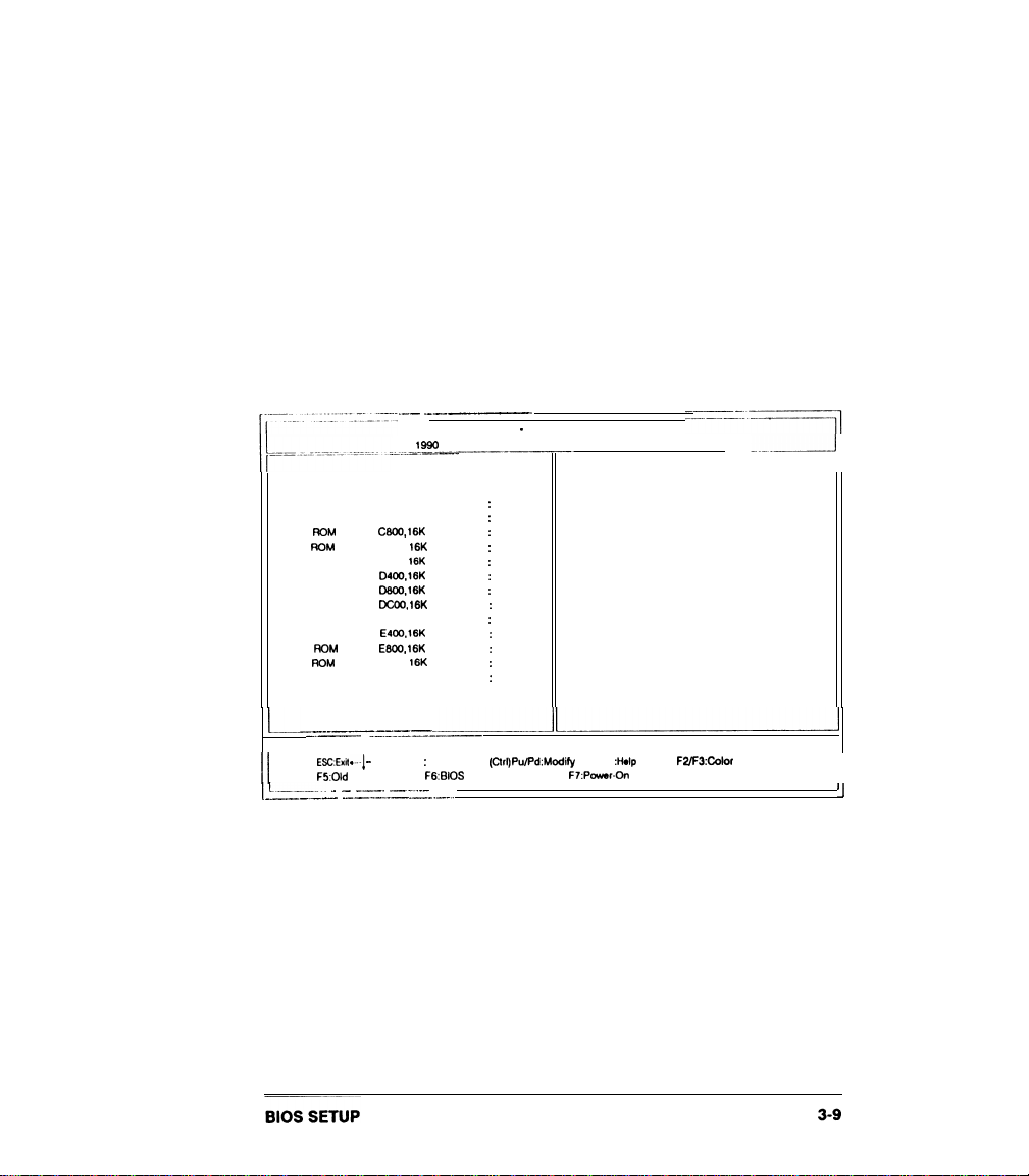
The ADVANCED CMOS SETUP option is used to set the
various system options for the user. The user can get various
options, some of which are listed below:
n
Weitek Processor
Ll
External Cache Memory
CI
Internal Cache Memory
II
Adaptor ROM Shadow
II
Shadow RAM
3-8
.
BIOS SETUP
Page 21
___ _----
BIOS SETUP PROGRAM - ADVANCED CMOS SETUP
(C)
1990
___._____~~-
____~-_---
Weitek Processor
External Cache Memory
Internal Cache Memory
Adaptor
ROM
Adaptor ROM Shadow CCOO, 16K
Adaptor ROM Shadow DOOO,
Adaptor ROM Shadow D400,16K
Adaptor ROM Shadow D800,16K
Adaptor ROM Shadow
Adaptor ROM Shadow EOOO, 16K
Adaplor ROM Shadow
Adaptor
Adaptor ROM Shadow ECOO, 16K
Shadow RAM Option
Shadow C800,16K
ROM
Shadow E800,16K
16K
DCOQ 16K
E400,16K
American Megalrends Inc., All Rights Reserved
_
__--_-.___J
II-------11
: Absent
:
Enabled
:
Enabled
:
Disabled
:
Disabled
:
Disabled
:
Disabled
:
Disabled
:
Disabled
:
Disabled
:
Disabled
:
Disabled
:
Disabled
:
Disabled
__________~
L-
______-
--------~
ESCExit *---I -
l
F5:Old
I/
1 L._____._ - - _.___ __-..--
__-__-
_-_----
Values
1 : Sel
_I----.
-LI
FGBIOS Setup Defaults
---
(Ctrl)Pu/Pd:Modify
F 1 :Hslp
F7:Power-On
Defaults
F27F3:Color
II
IJ
Page 22
Explanation of keys:
ESC : Exit to previous screen
Arrow keys: Cursor movement
PageUp/PageDown/Ctrl
value of the option by
PageUp/Ctrl
l/-1/10/-10.
If the option has less than
PageDown:
Modify the
10 available answers, then c Ctrl PageUP > is the same as
<
PageUP > and <
CtrlPageDown >
isthesameas <
PageDown >
Fl : Opiton for Help
F2/F3
:
Change Color
FS
:
Get the old values. These are the values with the user
starting from the current session. If the CMOS was good, then
the old values are the CMOS values, hense they are the BIOS
Setup default values.
F6
:
This will load all the Options in the Advanced CMOS
Setup/Advanced
Chipset
Setup with the BIOS Setup defaults
F7 : This will load all the Options in the Advanced CMOS
Setup/Advanced
Chipset
Setup with the Power-On defaults
.
WEITEK Processor
WEITEK coprocessor insert in socket
,preset
is set
When not inserted in socket, absent is set.
BIOS SETUP
Page 23

External Cache Memory
This function can be setup enable/disable External Cache
(second leave cache)
Internal Cache Memory
64/256KB.
This function can be setup enable/disable CPU Internal cache 8
KB
.
Adaptor RAM Shadow
Adaptor Shadow RAM address range from
C8000H
to
EFFFFH, each Block size at 16KB for enable or disable
Shadow RAM
There are four function that can be selected:
Video: Video shadow
Main
both
Disable
:
Main BIOS shadow
:
Video and Main BIOS Shadow
Disable shadow
:
(COOOO-C7FFFH)
(FOOOO”FFFFFH)
BIOS SETUP
3-11
Page 24
3-4 ADVANCED
CHIPSET
SETUP
The ADVANCED CHIPSET SETUP option is used to change
the register values for the
chipset
registers. The
chipset
registers control most of the system options in the computer.
Explanation keys:
ESC : Exit to previous screen
:
Arrow keys
PageUp/PageDown/Ctrl PageUp/Ctrl PageDown
the value of the option by
than 10 available answers, then <
< PageUp > and < CtrlPageDown > is same as < PageDown
Fl
:
Help for the option
F2/F3
F5
:
Get the old values. These are the values with the user
Cursor movement
:
Change Color
l/-1/10/-10.
Ctrl PageUp >
:
Modify
If the option has less
is same
as
>
starting from the current session. If the CMOS was good, then
the old values are the CMOS values, hence they are the BIOS
Setup default values.
F6 : This will load all the Options in the Advanced CMOS
Setup/Advanced
F7
:
This will load all the Options in the Advanced CMOS
Setup/Advanced
Chipset
Chipset
Setup with the BIOS Setup
defauhs
Setup with the Power-On defaults
3-12 BIOS SETUP
Page 25
_ __-_--.-~-
__-.
1
- -.-----------_---
Non-Cacheable Block- 1 Size
Non-Cacheable Block-l
Non-Cacheable Block-2 Size
Non-Cacheable Block-2 Base
Cacheable
Video BIOS Area
__._ _-_ - -~-----
__.
_--_
-
_-___-----__~-
(C)
1990
RAM
Address Range
Cacheable
ESC:Exit
f
F5:Old
Values
BIOS Setup Program -
American Megatrends Inc., All Rights
Base
_._.
AMI
BIOS Utilities
--
:
Disabled
:OKB
:
Disabled
:OKB
;8MB
:
Y8S
1 .-:
Sel
Ctrl) Pu/Pd: Modify
F6: BIOS Setup Defaults
Reserved
Fl
:
Help F2/F3:
R:
Power-On Defaults
Color
II
BIOS SETUP
3-l 3
Page 26

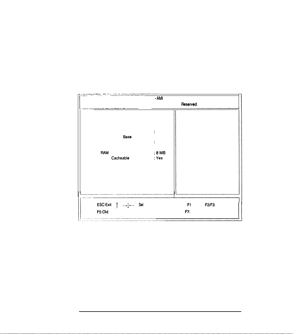
Non-Cacheable Block Size
This setup for set Non-Cacheable block size of
64/128/256/5 12K/Disable
Non-Cacheable Block Base
This setup for set Non-Cacheable Block Starting address for
example, if a
address is a multiple of
Cacheable RAM Address Range
512KB
non-cacheable block is selected its starting
512KB
This Cacheable DRAM size, you can select from range
(l-64MB)
Video BIOS Area Cacheable
Enable or Disable Video BIOS Cacheable
Please check your VGA card, If OAK VGA card (slow speed),
this function must disable
3-l 4
BIOS SETUP
Page 27
3-5.
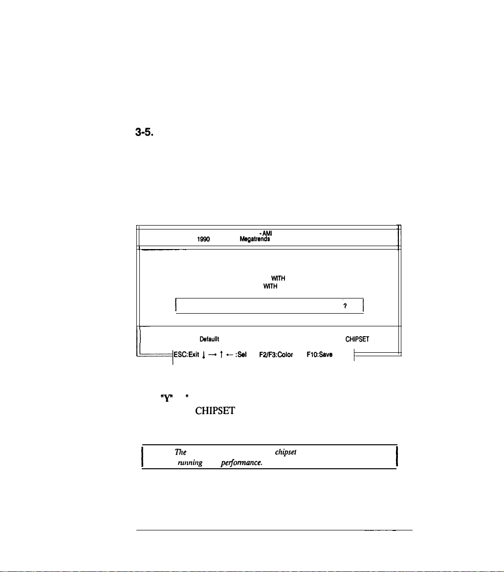
AUTO CONFIGURATION WITH BIOS
DEFAULTS
When you enter AUTO CONFIGURATION WITH BIOS
DEFAULTS, the screen will be as follows:
BIOS SETUP PROGRAM -
(C)
1
Load BIOS Setup Default Values from ROM Table (Y/N)
Load BIOS Setup
ESC:Exit
Press
“Y”
or ’ N” to change ADVANCED CMOS SETUP and
ADVANCED
Note:
Tote
BIOS default values, setup
I
mnning high pegonnance.
AMI
1990
American
AUTO CONFIGURATION
AUTO CONFIGURATION
Defaullt
1 - 1
CHIPSET
Megatrends
STANDARD CMOS SETUP
ADVANCED CMOS SETUP
Values for Advanced CMOS and Advanced
-
:Sel FZIF3:Color FlO:Save
SETUP with BIOS default values.
BIOS SETUP UTILITIES
Inc., All Rights Reserved
WlTH
BIOS DEFAULTS
WlTH
POWER-ON DEFAULTS
chipset
register for
.?
N
CHIPSET
& Exit
r
mainboard
1
Setup
I
BIOS SETUP
--- ~
3-l 5
Page 28
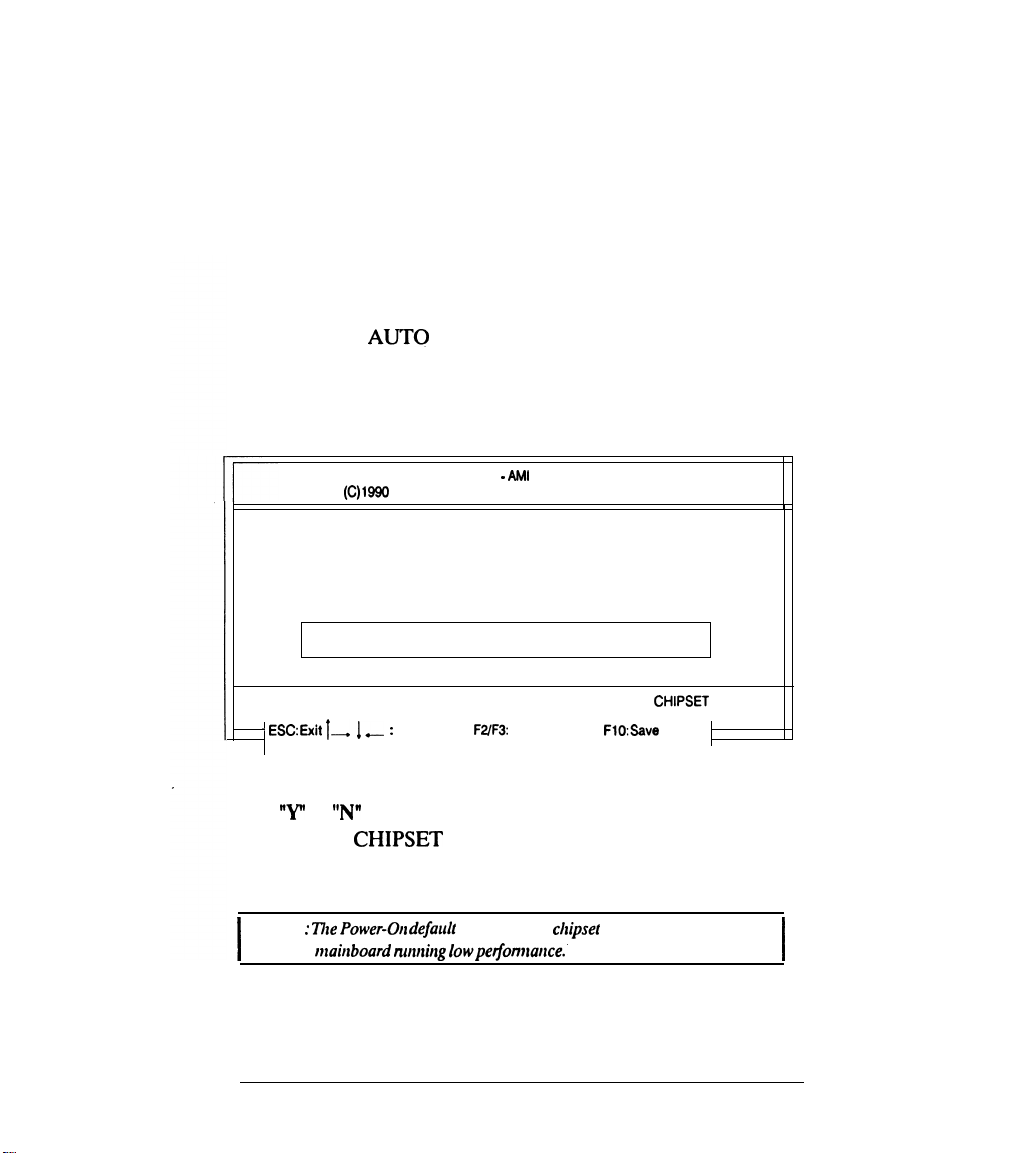
3-6 AUTO CONFIGURATION WITH POWER-ON
DEFAULTS.
When you enter
AUTO)
CONFIGURATION WITH
POWER-ON DEFAULTS, the screen will be as follows:
BIOS SETUP PROGRAM
(C)l990 American Megatrends Inc., All Rights Reserved
STANDARD CMOS SETUP
AUTO CONFIGURATION WITH BIOS DEFAULTS
AUTO CONFIGURATION WITH POWER-ON DEFAULTS
Load Power-On Default Values from ROM Table (Y/N) ? N
Load Power-On Default Values for Advanced CMOS and Advanced
-
ESCExit
Press
“Y”
or
I__-.
“NW
I._ :
ADVANCED CMOS SETUP
Sel
to change ADVANCED CMOS SETUP and
- AM
BIOS SETUP UTILITIES
FYF3:
Color
F1O:Save
CHIPSET
& Exit
Setup
ADVANCED CHIPSET SETUP with Power-on default values.
I
3-16
Note :
77le Power-011 default
mairtboard nrrtrtirtg lowperfomrartce.’
values, setup
chipset
register for
I
BIOS SETUP
Page 29

3-9. WRITE TO CMOS AND EXIT
The options set in the Standard Setup, Advanced Setup,
Advanced Chip-set Setup and the New Password (if it has been
changed) are stored in the CMOS. The CMOS checksum is
calculated and written into the CMOS. After that, control is
passed back to the BIOS.
3-10.
DO NOT WRITE TO CMOS AND EXIT
Control is passed back to the BIOS without writing to the
CMOS.
BIOS SETUP
3-17
 Loading...