

Cherry Semiconductor CS8391YDPR5, CS8391YDP5 Datasheet
1
Features
■ 5V, 250mA Primary Output
■ 5V, 100mA Secondary
Output
■ 3% Tolerance, Both
Outputs
■ ON/OFF Control for
Primary Output
■ Low Quiescent Current
Drain (100µA V
OUT2
)
■ Low Reverse Current
■ Protection Features
Reverse Battery (-15V)
Short Circuit
Overtemperature
Package Options
CS8391
5V/250mA, 5V/100mA Micropower
Low Dropout Regulator with ENABLE
CS8391
Description
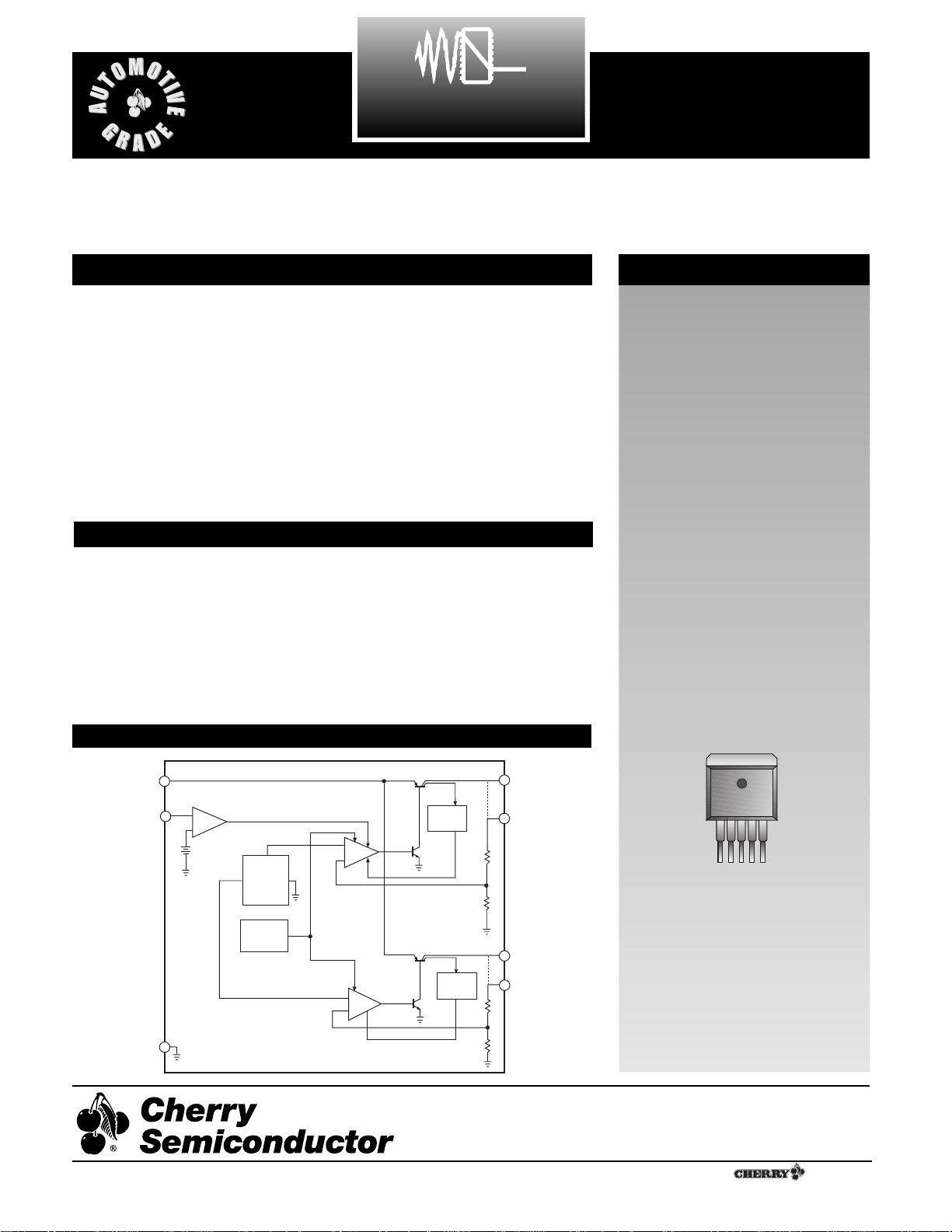
Block Diagram
Absolute Maximum Ratings
Input Voltage.....................................................................................-15V to 45V
Power Dissipation.................................................................Internally Limited
Operating Temperature Range................................................-40¡C to +125¡C
Maximum Junction Temperature ...........................................-40¡C to +150¡C
Storage Temperature Range ....................................................-55¡C to +150¡C
Electrostatic Discharge (Human Body Model) ..........................................4kV
Lead Temperature Soldering
Wave Solder (through hole styles only)..........10 sec. max, 260¡C peak
Reflow (SMD styles only)...........60 sec. max above 183¡C, 230¡C peak
The CS8391 is a precision, dual 5V
micropower linear voltage regulator. The switched primary output
(V
OUT1
) supplies up to 250mA
while the secondary (V
OUT2
) is
capable of supplying 100mA. Both
outputs have a maximum dropout
voltage of 600mV and low reverse
current. Quiescent current drain is
typically 150µA when supplying
100µA from each output.
The ENABLE input provides logic
level control of the primary output.
With the primary output disabled,
quiescent current drain is typically
100µA when supplying 100µA from
the secondary output.
The CS8391 is extremely robust
with protection provided for
reverse battery, short circuit, and
overtemperature on both outputs.
The CS8391 is available in a 5-lead
D2PAK.
5 Lead D2PAK
Tab (Gnd)
1
Consult factory for 8L and 16L SO, 8L and
16L PDIP, 7L D
2
PAK and 5L TO-220.
1. V
IN
2. V
OUT1
3. Gnd
4. V
OUT2
5. ENABLE
A Company
¨
Rev. 1/12/98
Cherry Semiconductor Corporation
2000 South County Trail, East Greenwich, RI 02818
Tel: (401)885-3600 Fax: (401)885-5786
Email: info@cherry-semi.com
Web Site: www.cherry-semi.com
V
ENABLE
IN
+
-
Bandgap
Reference
Thermal
Shutdown
+
-
+
-
Primary Output
Secondary Output
Current
Limit
Current
Limit
V
OUT
*
V
OUT
*Note: Internally
connected on 5 leaded
package.
V
OUT
*
V
OUT
1
Sense
1
2
Sense
2
Gnd
2
CS8391
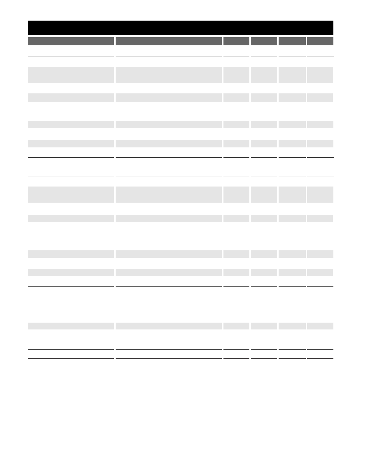
PARAMETER TEST CONDITIONS MIN TYP MAX UNIT
Electrical Characteristics: 6V ² VIN² 26V, I
OUT1
= I
OUT2
= 100µA, -40¡C ² TC² 125ûC, -40¡C ² TJ² 150ûC unless otherwise specified
■ Primary Output Stage (V
OUT1
)
Output Voltage, V
OUT1
100µA ² I
OUT1
² 250mA 4.85 5.00 5.15 V
Dropout Voltage I
OUT1
= 250mA 400 600 mV
I
OUT1
= 100µA 100 150 mV
Line Regulation 6V ² V
IN
² 26V 5 50 mV
Load Regulation 1mA ² I
OUT1
² 250mA, VIN= 14V 5 50 mV
Quiescent Current ENABLE = HIGH, V
IN
= 16V, 22 50 mA
I
OUT1
= 250mA
Ripple Rejection f = 120Hz, I
OUT1
= 125mA, 7V ² VIN² 17V 60 70 dB
Current Limit 260 400 mA
Short Circuit Current Limit V
OUT1
= 0V, VIN= 16V 25 mA
Reverse Current V
OUT1
= 5V, VIN= 0V 100 1500 µA
■ Secondary Output (V
OUT2
)
Output Voltage, V
OUT2
100µA ² I
OUT2
² 100mA 4.85 5.00 5.15 V
Dropout Voltage I
OUT2
= 100mA 400 600 mV
I
OUT2
= 100µA 100 150 mV
Line Regulation 6V ² V
IN
² 26V 5 50 mV
Load Regulation 100µA ² I
OUT2
² 100mA, VIN= 14V 5 50 mV
Quiescent Current ENABLE = LOW, V
IN
= 12.8V 100 150 µA
ENABLE = HIGH, V
IN
= 16V, 8 25 mA
I
OUT2
= 100mA
Ripple Rejection f = 120Hz, I
OUT2
= 50mA, 7V ² VIN² 17V 60 70 dB
Current Limit 105 200 mA
Short Circuit Current Limit V
OUT2
= 0V, VIN= 16V, I
OUT1
= 0A 25 mA
Reverse Current V
OUT2
= 5V, VIN= 0V 100 250 µA
■ Enable Function (ENABLE)
Input Threshold ENABLE = LOW, 7V ² V
IN
² 26V 1.2 0.8 V
ENABLE = HIGH, 7V ² V
IN
² 26V 2.0 1.2 V
Input Bias Current 0V ² V
ENABLE
²5V -2 0 2 µA
■ Protection Circuits
Overtemperature Threshold (Guaranteed by Design) 150 180 ¡C
 Loading...