

Cherry Semiconductor CS8371ETVA7, CS8371ET7 Datasheet
1
Features
■ Two Regulated Outputs
8V ±5%, 1A
5V ±5%, 250mA
■ Independent ENABLE for
each Output
■ Separate Sense Feedback
Lead for 8V Output
■ <10µA Sleep Mode Current
■ Fault Protection
Overvoltage Shutdown
+45V Peak Transient
Voltage
Short Circuit
Thermal Shutdown
■ CMOS Compatible, Low-
Current ENABLE Inputs
Package Options
TO-220 7 Lead
Tab (Gnd)
CS8371
8V/1A, 5V/250mA Dual Regulator with
Independent Output Enables and NoCapª
CS8371
Description
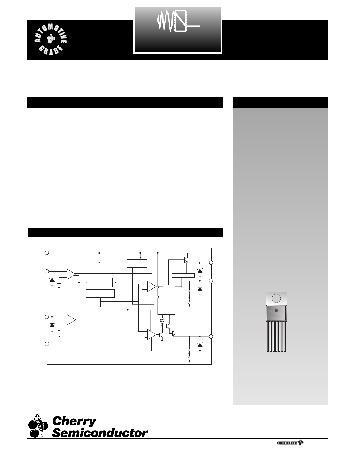
Block Diagram
The CS8371 is a 8V/5V dual output
linear regulator. The 8V ±5% output
sources 1A, while the 5V ±5% output sources 250mA. Each output is
controlled by its own ENABLE
lead. Setting the ENABLE input
high turns on the associated regulator output. Holding both ENABLE
inputs low puts the IC into sleep
mode where current consumption
is less than 10µA.
The regulator is protected against
overvoltage, short-circuit and ther-
mal runaway conditions. The
device can withstand 45V load
dump transients making suitable
for use in automotive environments. CherryÕs proprietary
NoCapª solution is the first technology which allows the output to
be stable without the use of an
external capacitor.
The CS8371 is available in a 7 lead
TO-220 package with copper tab.
The tab can be connected to a
heatsink if necessary.
1 ENABLE
1
2 ENABLE
2
3V
OUT2
4 Gnd
5 Sense
6V
CC
7V
OUT1
Rev. 6/9/99
Cherry Semiconductor Corporation
2000 South County Trail, East Greenwich, RI 02818
Tel: (401)885-3600 Fax: (401)885-5786
Email: info@cherry-semi.com
Web Site: www.cherry-semi.com
A Company
¨
NoCap is a trademark of Cherry Semiconductor Corporation, and is patented.
Pre-Regulator/
Bias Generator
Trimmed Bandgap
Voltage Reference
Thermal
Shutdown
ENABLE
ENABLE
V
Gnd
CC
1
2
-
+
1.2V
-
+
1.2V
Overvoltage
Shutdown
Current Limit
+
VIA
-
-
+
Current Limit
V
OUT1
Sense
V
OUT2
1
2
CS8371
PARAMETER TEST CONDITIONS MIN TYP MAX UNIT
Electrical Characteristics: -40¡C ² TA² +85¡C, 10.5V ² VCC² 16.0V, ENABLE1= ENABLE2= 5.0V,
I
OUT1
= I
OUT2
= 5.0mA, unless otherwise stated.
■ Primary Output (V
OUT1
)
Output Voltage I
OUT1
= 1.0A 7.60 8.00 8.40 V
Line Regulation 10.5V ² VCC² 26V 50 mV
Load Regulation 5mA ² I
OUT1
² 1.0A 150 mV
Sleep Mode Quiescent VCC= 14V, ENABLE1= ENABLE2= 0V 0 0.2 10.0 µA
Current
Quiescent Current VCC= 14V, I
OUT1
= 1.0A, I
OUT2
= 250mA 30 mA
Dropout Voltage I
OUT1
= 250mA 1.2 V
Dropout Voltage I
OUT1
= 1.0A 1.5 V
Quiescent Bias Current I
OUT1
= 5mA, ENABLE2= 0V, VCC= 14V 10 mA
IQ= ICC- I
OUT1
Quiescent Bias Current I
OUT1
= 1.0A, ENABLE2= 0V, VCC= 14V 22 mA
IQ= ICC- I
OUT1
Ripple Rejection f = 120Hz, VCC= 14V with 1.0VPPAC, 90 dB
C
OUT
= 0µF
f = 10kHz, VCC= 14V with 1.0VPPAC, 74 dB
C
OUT
= 0µF
f = 20kHz, VCC= 14V with 1.0VPPAC, 68 dB
C
OUT
= 0µF
Current Limit VCC= 16V 1.1 2.5 A
Overshoot Voltage 5mA ² I
REG1
² 1.0A 6.0 V
Output Noise 10Hz-100kHz 300 µV
rms
■ Secondary Output (V
OUT2
)
Output Voltage I
OUT2
= 250mA 4.75 5.00 5.25 V
Line Regulation 7V ² VCC² 26V 40 mV
Load Regulation 5mA ² I
OUT2
² 250mA 100 mV
Dropout Voltage I
OUT2
= 5.0mA 2.2 V
Dropout Voltage I
OUT2
= 250mA 2.5 V
Quiescent Bias Current I
OUT2
= 5mA, ENABLE1= 0V, VCC= 14V 7 mA
IQ= ICC- I
OUT2
Quiescent Bias Current I
OUT2
= 250mA, ENABLE1= 0V, VCC= 14V 8 mA
IQ= ICC- I
OUT2
Ripple Rejection f = 120Hz, VCC= 14V with 1.0 VPPAC, 90 dB
C
OUT
= 0µF
f= 10kHz, VCC= 14V with 1.0VPPAC, 75 dB
C
OUT
= 0µF
f = 20kHz, VCC= 14V with 1.0VPPAC, 67 dB
C
OUT
= 0µF
Absolute Maximum Ratings
Power Dissipation.............................................................................................................................................Internally Limited
ENABLE Input Voltage Range .............................................................................................................................-0.6V to +10.0V
Load Current (8V Regulator)...........................................................................................................................Internally Limited
Load Current (5V Regulator)...........................................................................................................................Internally Limited
Transient Peak Voltage (31V load dump @ 14V V
CC
) ...........................................................................................................45V
Storage Temperature Range ................................................................................................................................-65¡C to +150¡C
Junction Temperature Range...............................................................................................................................-40¡C to +150¡C
Lead Temperature Soldering: Wave Solder (through hole styles only)..........................................10 sec. max, 260¡C peak
3
Electrical Characteristics: -40¡C ² TA² +85¡C, 10.5V ² VCC² 16.0V, ENABLE1= ENABLE2= 5.0V,
I
OUT1
= I
OUT2
= 5.0mA, unless otherwise stated.
CS8371
Package Pin Description
PACKAGE PIN # PIN SYMBOL FUNCTION
7 Lead TO-220
1 ENABLE
1
ENABLE control for the 8V, 1A output
2 ENABLE
2
ENABLE control for the 5V, 250mA output
3V
OUT2
5V ±5%, 250mA regulated output
4 Gnd Ground
5 Sense Sense feedback for the primary 8V output
6V
CC
Supply voltage, usually from battery
7V
OUT1
8V ±5%, 1A regulated output
PARAMETER TEST CONDITIONS MIN TYP MAX UNIT
■ Secondary Output (V
OUT2
): continued
Current Limit VCC= 16V 270 600 mA
Overshoot Voltage 5mA ² I
REG2
² 250mA 4.3 V
Output Noise 10Hz-100kHz 170 µV
rms
■ ENABLE Function (ENABLE)
Input Current VCC= 14V, 0V ² ENABLE ² 5.5V -150 150 µA
Input Voltage Low 0 0.8 V
High 2.0 5.0 V
■ Protection Circuitry
ESD Threshold Human Body Model ±2.0 ±4.0 kV
Overvoltage Shutdown 24 30 V
Thermal Shutdown Guaranteed by Design 150 180 ¡C
Thermal Hysteresis 30 ¡C
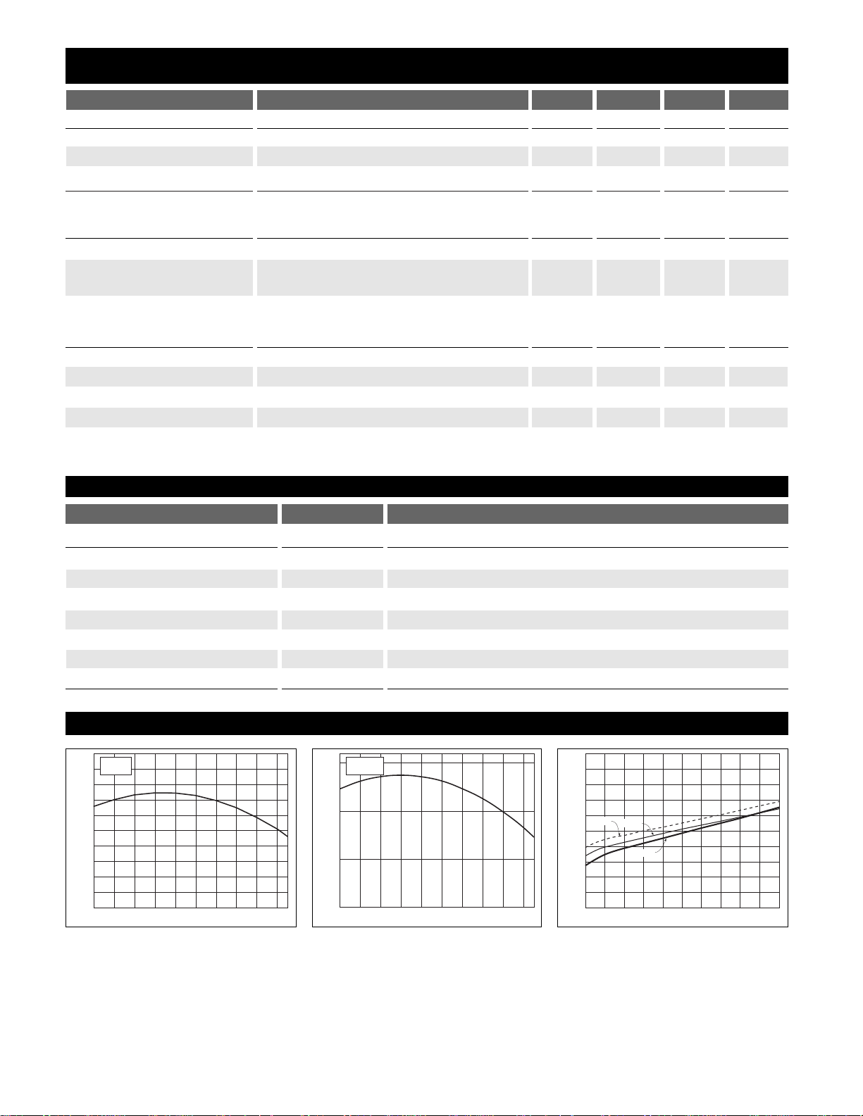
Typical Performance Characteristics
Regulator 1 Output Voltage Regulator 2 Output Voltage
Regulator 1 Dropout Voltage
8.05
VIN = 14V
8.04
= 1A
I
OUT
8.03
8.02
8.01
8.00
7.99
Output Voltage (V)
7.98
7.97
7.96
7.95
-40 -20 0 20 40 60 80 100 120 140
Ambient Temperature (°C)
5.00
4.95
Output Voltage (V)
4.90
4.85
-40 -20 0 20 40 60 80 100 120 140
VIN = 14V
= 250A
I
OUT
Ambient Temperature (°C)
2.0
1.8
1.6
1.4
1.2
-40°C
1.0
0.8
Dropout Voltage (V)
0.6
0.4
0.2
0
25°C
85°C
0 100 200 300 400 500 600 700 800 900
Output Current (mA)
1000
 Loading...