

Cherry Semiconductor CS8361YT7, CS8361YN16, CS8361YDWR20, CS8361YDWFR16, CS8361YDWF16 Datasheet
...
1
Features
■ 2 Regulated Outputs
Standby Output 5V
±2%; 100mA
Tracking Output 5V;
250mA
■ Low Dropout Voltage
(0.4V at rated current)
■ RESET Option
■ ENABLE Option
■ Low Quiescent Current
■ Protection Features
Independent Thermal
Shutdown
Short Circuit
60V Load Dump
Reverse Battery
Package Options
7L TO-220
CS8361
5V Dual Micropower Low Dropout
Regulator with ENABLE and RESET
CS8361
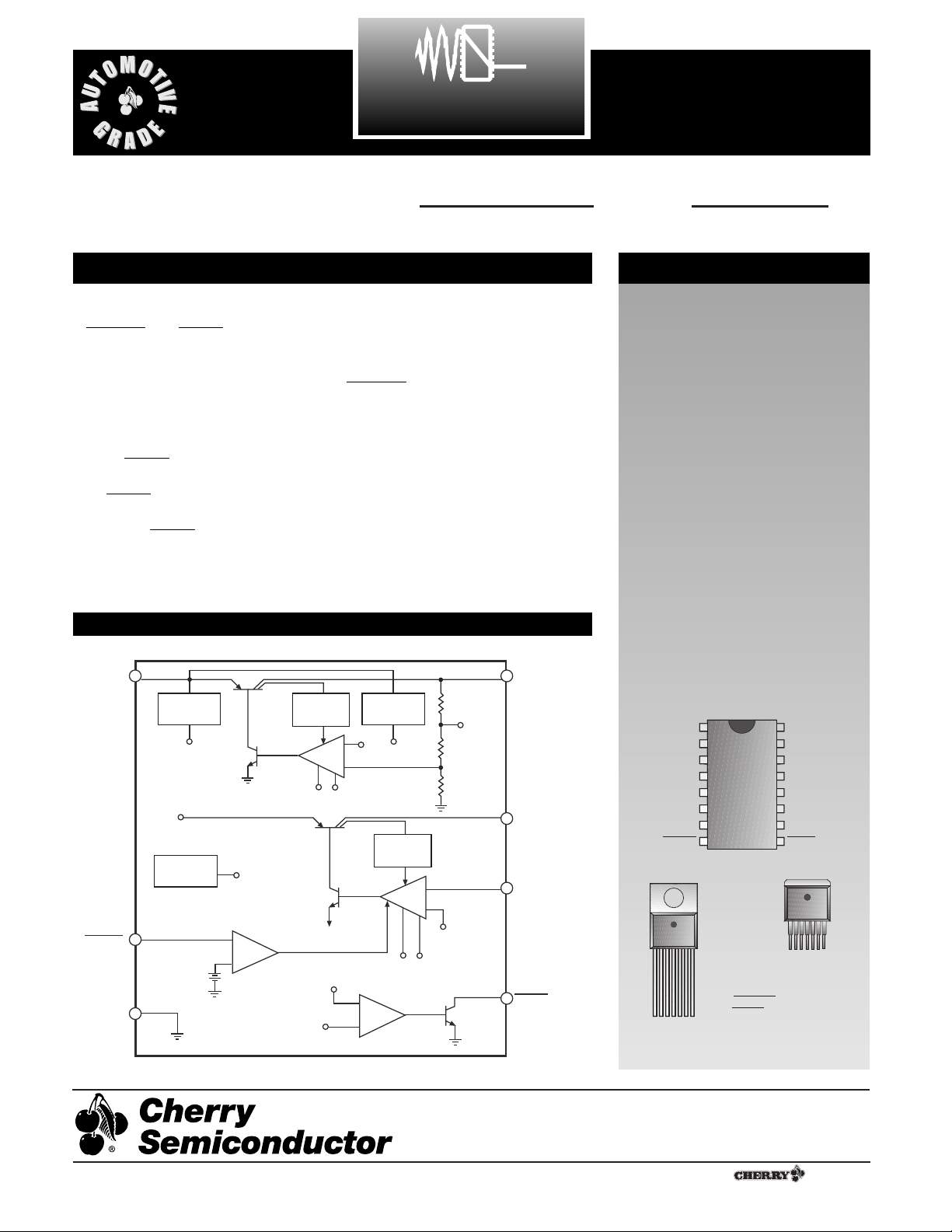
Block Diagram
Description
7L D2PAK
1
16 Lead PDIP & SOIC Wide
(internally fused leads)
NC
NC
NC
NC
NC
NC
V
IN
Gnd
Gnd
Gnd
Gnd
V
TRK
Adj
ENABLE
RESET
V
STBY
1. V
STBY
2. V
IN
3. V
TRK
4. Gnd
5. Adj
6. ENABLE
7. RESET
Also available in 20 Lead SOIC Wide.
Consult factory for 20 Lead PSOP .
* Consult factory for positive ENABLE option.
Rev. 5/4/99
The CS8361 is a precision micropower dual voltage regulator with
and .
The 5V standby output is accurate
within ±2% while supplying loads
of 100mA and has a typical
dropout voltage of 400mV.
Quiescent current is low, typically
140µA with a 300µA load. The
active output monitors the
5V standby output and holds
the line low during powerup and regulator dropout conditions. The circuit includes
hysteresis and is guaranteed to
operate correctly with 1V on the
standby output.
The second output tracks the 5V
standby output through an external
adjust lead, and can supply loads
of 250mA with a typical dropout
voltage of 400mV. The logic level
lead is used to control
this tracking regulator output.
Both outputs are protected against
overvoltage, short circuit, reverse
battery and overtemperature conditions. The robustness and low quiescent current of the CS8361 makes
it not only well suited for automotive microprocessor applications,
but for any battery powered microprocessor applications.
ENABLE
RESET
RESET
RESET
RESETENABLE
Cherry Semiconductor Corporation
2000 South County Trail, East Greenwich, RI 02818
Tel: (401)885-3600 Fax: (401)885-5786
Email: info@cherry-semi.com
Web Site: www.cherry-semi.com
A Company
®
V
IN
Overvoltage
Shutdown
OVSD
Current
Limit
Bandgap
BG
BG
+
–
RESET
V
STBY
5V,100mA,2%
1
V
IN
Thermal
Shutdown
ENABLE
Gnd
–
+
TSD
TSD
RESET
BG
OVSD
V
TRK
Current
Limit
–
+
V
STANDBY
OVSD
TSD
+
–
250mA
Adj
RESET
1
2
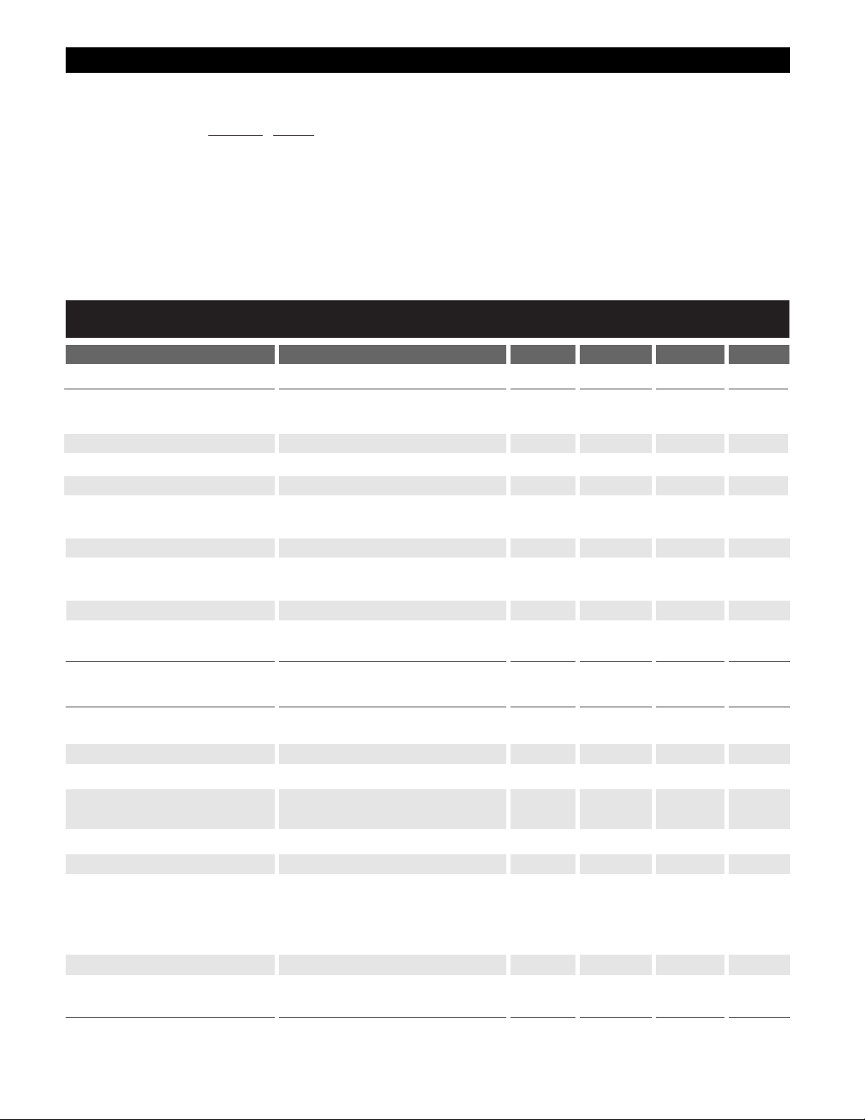
Electrical Characteristics: 6V ² V
IN
² 26V, I
OUT1
= I
OUT2
= 100µA, -40¡C ² TA ²+125¡C, -40¡C ²TJ² +150¡C,
unless otherwise specified.
PARAMETER TEST CONDITIONS MIN TYP MAX UNIT
CS8361
Absolute Maximum Ratings
Supply Voltage, V
IN
.....................................................................................................................................................-16V to 26V
Positive Transient Input Voltage, tr > 1ms.............................................................................................................................60V
Negative Transient Input Voltage, T < 100ms, 1% Duty Cycle..........................................................................................-50V
Input Voltage Range ( , ) ...............................................................................................................-0.3V to 10V
Junction Temperature...........................................................................................................................................-40¡C to +150¡C
Storage Temperature Range................................................................................................................................-55¡C to +150¡C
ESD Susceptibility (Human Body Model)..............................................................................................................................2kV
Lead Temperature Soldering
Wave Solder (through hole styles only) .....................................................................................10 sec. max, 260¡C peak
Reflow (SMD styles only) ......................................................................................60 sec. max above 183¡C, 230¡C peak
RESETENABLE
■ Tracking Output (V
TRK
)
V
STBY
Ð V
TRK
, 6V ² VIN² 26V -25 +25 mV
V
TRK
Tracking Error 100µA ² I
TRK
² 250mA (note 1)
Adjust Pin Current, I
Adj
Loop in Regulation 1.5 5 µA
Line Regulation 6V ² VIN² 26V (note 1) 5 50 mV
Load Regulation 100µA ² I
TRK
² 250mA (note 1) 5 50 mV
Dropout Voltage (VINÐ V
TRK
) I
TRK
= 100µA 100 150 mV
I
TRK
= 250mA 400 700 mV
Current Limit VIN= 12V, V
TRK
= 4.5 275 500 mA
Quiescent Current VIN= 12V, I
TRK
= 250mA 25 50 mA
No Load on V
STBY
Reverse Current V
TRK
= 5V, VIN= 0V 200 1500 µA
Ripple Rejection f = 120Hz, I
TRK
= 250mA 60 70 dB
7V ² VIN² 17V
■ Standby Output (V
STBY
)
Output Voltage, V
STBY
6V ² VIN² 26V 4.90 5.00 5.10 V
100µA ² I
STBY
² 100mA
Line Regulation 6V ² VIN² 26V 5 50 mV
Load Regulation 100µA ² I
STBY
² 100mA 5 50 mV
Dropout Voltage (VINÐ V
STBY
) I
STBY
= 100µA 100 150 mV
I
STBY
= 100mA 400 600 mV
Current Limit VIN= 12V, V
STBY
= 4.5V 125 200 mA
Short Circuit Current VIN= 12V, V
STBY
= 0V 10 100 mA
Quiescent Current V
IN
= 12V, I
STBY
= 100mA 10 20 mA
I
TRK
= 0mA
V
IN
= 12V, I
STBY
= 300µA 140 200 µA
I
TRK
= 0mA
Reverse Current V
STBY
= 5V, VIN= 0V 100 200 µA
Ripple Rejection f = 120Hz, I
STBY
= 100mA 60 70 dB
7V ² VIN² 17V
Note 1: V
TRK
connected to Adj lead. V
TRK
can be set to higher values by using an external resistor divider.
 Loading...