

Cherry Semiconductor CS8271YN8, CS8271YDR8, CS8271YD8 Datasheet
1
Features
■ Low Quiescent Current
■ Adjustable Output:
5V to 12V
■ for Sleep Mode
Control
■ 100mA Output Current
Capability
■ Fault Protection
+60V Load Dump
-15V Reverse Voltage
Short Circuit
Thermal Shutdown
■ Low Reverse Current
(Output to Input)
ENABLE
Package Options
CS8271
CS8271
Description
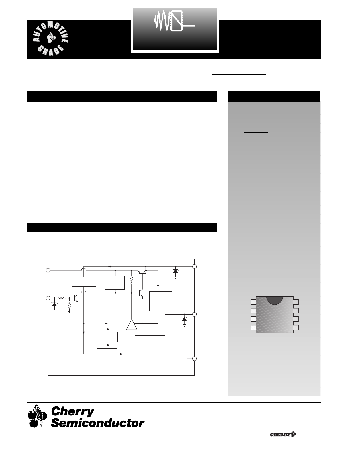
The CS8271 is an adjustable micropower voltage regulator with very
low quiescent current (60µA typical
at 100µA load). The output supplies
100mA of load current with a maximum dropout voltage of only
600mV. Control logic includes
. The combination of low
quiescent current, outstanding regulator performance and control
logic makes the CS8271 ideal for
any battery operated equipment.
The logic level compatible
pin allows the user to put the regu-
lator into a shutdown mode where it
draws only 50µA of quiescent current.
The regulator is protected against
reverse battery, short circuit, over
voltage, and over temperature conditions. The device can withstand
60V load dump transients making it
suitable for use in automotive environments.
The CS8271 is pin compatible with
the National Semiconductor
LM2931.
ENABLE
ENABLE
Block Diagram
1
V
OUT
Gnd
NC
Adj
V
IN
NC
NC
ENABLE
Other Packages: Consult factory for
16L SO Batwing, 5L TO-220 and D
2
PAK.
8L SOIC & PDIP
Adjustable Micropower Low Dropout
Linear Regulator with
ENABLE
A Company
¨
Rev. 3/26/97
Cherry Semiconductor Corporation
2000 South County Trail, East Greenwich, RI 02818
Tel: (401)885-3600 Fax: (401)885-5786
Email: info@cherry-semi.com
Web Site: www.cherry-semi.com
V
ENABLE
Input
V
IN
Current Source
(Circuit Bias)
Over
Voltage
Shutdown
OUT
Current Limit
Thermal
Shutdown
Bandgap
Reference
+ -
Error
Amplifier
Sense
Adj
Gnd
2
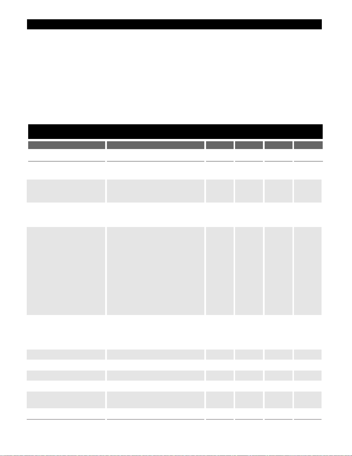
Power Dissipation.............................................................................................................................................Internally Limited
Transient Input Voltage ..................................................................................................................................................-50V, 60V
Reverse Battery..........................................................................................................................................................................-15V
Output Current .................................................................................................................................................Internally Limited
ESD Susceptibility (Human Body Model)..............................................................................................................................2kV
Junction Temperature .............................................................................................................................................-40¡C to 150¡C
Storage Temperature...............................................................................................................................................-55¡C to 150¡C
Lead Temperature Soldering
Wave Solder (through hole styles only) .....................................................................................10 sec. max, 260¡C peak
Reflow (SMD styles only) ......................................................................................60 sec. max above 183¡C, 230¡C peak
Adj and Enable Output ..................................................................................................................................................-0.3V, 10V
V
OUT
...........................................................................................................................................................................-0.3V, 20V
PARAMETER TEST CONDITIONS MIN TYP MAX UNIT
Absolute Maximum Ratings
Electrical Characteristics: V
OUT
+ 1V ² VIN² 30V, 5V ² V
OUT
² 12V, I
OUT
= 10mA, -40¡ ² TA ² 125¡, -40¡ ² TJ ² 150¡,
V
ENABLE
= 0V; unless otherwise specified.
CS8271
■ Output Voltage
Dropout Voltage I
OUT
= 100µA, V
DROP
= (VINÐ V
OUT
) 100 150 mV
I
OUT
= 100mA, V
DROP
= (VINÐ V
OUT
) 400 600 mV
Load Regulation Measure V
OUT
when 0.1 1.0 %V
OUT
I
OUT
= 100µA, 100mA.
LD
REG
= ABS (ÆV
OUT
)
Line Regulation I
OUT
= 1mA. Measure V
OUT
0.1 0.5 %V
OUT
when VIN= V
OUT
+ 1V, 30V.
LN
REG
= ABS (ÆV
OUT
)
Quiescent Current, (IQ)V
IN
= 6V, I
OUT
= 100µA, 55 120 µA
Active Mode V
OUT
setup for 5V. IQ= IVIN- I
OUT
VIN= 13V, I
OUT
= 100µA, 130 200 µA
V
OUT
setup for 12V. IQ= IVIN- 100µA
VIN= 30V, I
OUT
= 100µA, 150 450 µA
V
OUT
setup for 5V, IQ= IVIN- 100µA
VIN= 30V, I
OUT
= 100µA, 200 500 µA
V
OUT
setup for 12V, IQ= IVIN- 100µA
I
OUT
= 50mA, IQ= IVIN- 50mA 4 7 mA
I
OUT
= 100mA, IQ= IVIN- 100mA 12 21 mA
Quiescent Current, (IQ)V
IN
= 6V, ENABLE = 2.5V, 20 50 µA
Sleep Mode I
QSLEEP
= IV
IN
VIN= 30V, ENABLE = 2.5V, 75 350 µA
I
QSLEEP
= IV
IN
Ripple Rejection f=120Hz, (Note 1) 60 75 dB
Current Limit V
OUT
= V
OUT
- 500mV, I
LIM
= IV
OUT
105 200 300 mA
Short Circuit Output Current V
OUT
=0V, I
SHRT
= IV
OUT
15 100 215 mA
Thermal Limit (Note 1) 150 180 210 ¡C
Overvoltage Shutdown Adjust VINfrom 28V to 40V 30 34 38 V
until V
OUT
²1V
Reverse Current VIN=0V, I
REV
= IV
OUT
, V
OUT
= 13.2V 100 200 µA
 Loading...