

Cherry Semiconductor CS8240YTFVA5 Datasheet
1
Features
■ Low Output Saturation
Voltage
0.22V at I
OUT
= 125mA
0.33V at I
OUT
= 225mA
■ Overmolded Package
■ On-Chip Flyback Diode
■ Fault Protection
Over voltage
Shutdown (32V, typ)
Thermal Shutdown
(165¡C, typ)
Short Circuit Limiting
(1.1A typ)
-50V Reverse Transient
Protection
60V Load Dump
Protection
Reverse Battery
■ Low Quiescent Current
(Off State)
■ ESD Protected
Package Options
5 Lead TO-220
Overmolded
CS8240
500mA High Side (PNP) Driver
with On-
Chip Flyback Diode
Description
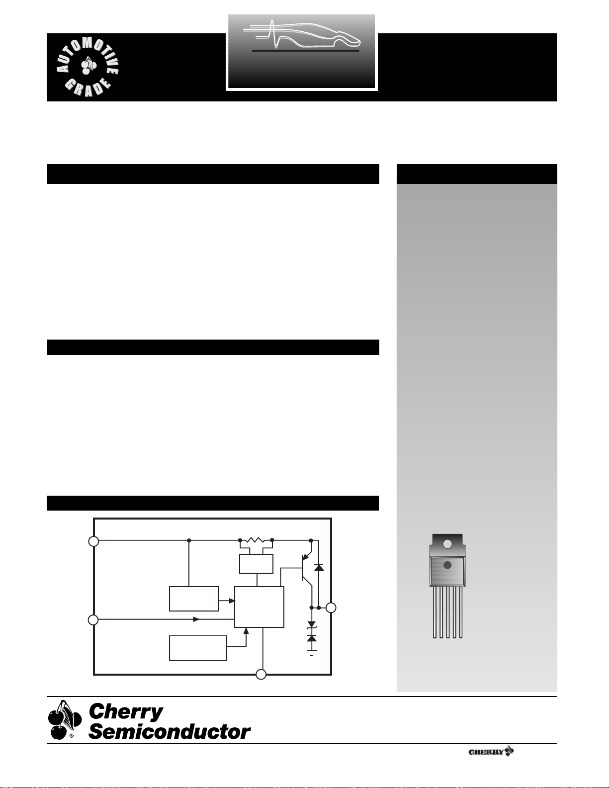
Block Diagram
Absolute Maximum Ratings
The CS8240 is a fast, PNP high side
driver capable of delivering up to
500mA into a resistive or inductive
load in harsh automotive or industrial
environments. An internal flyback
diode clamp is incorporated for inductive loads. The input (V
IN
) is TTL and
CMOS compatible and has hysteresis to
minimize the effects of noise. When the
input is high, the output is on. When
the input is low, the output is off and
the supply voltage quiescent current is
very low (<1.0µA, typ). For device protection, the CS8240 incorporates thermal shutdown, short circuit current
limiting, over voltage shutdown, and
reverse battery protection. The CS8240
can withstand supply voltage transients of 60V (min) and -50V.
The CS8240 is available in an overmolded 5 lead TO-220 package and is a competitive replacement for the LM-1921,
LM-1951, LM-1952, MC-3399, and L-9350.
CS8240
Supply Voltage.....................................................................................6V to +26V
Overvoltage Protection....................................................................................60V
Reverse Voltage ........................................................................................-16V DC
.........................................................................................-50V Transient
Internal Power Dissipation .....................................................Internally limited
Logic Input Voltage ..........................................................................-0.3V to 7.0V
Junction Temperature Range.....................................................-40¡C to +150¡C
Storage Temperature Range ......................................................-55¡C to +165¡C
Lead Temperature Soldering
Wave Solder(through hole styles only).............10 sec. max, 260¡C peak
Electrostatic Discharge (Human Body Model) ............................................2kV
1V
CC
2 OUT
3NC
4 Gnd
5V
IN
1
A Company
¨
Rev. 1/27/98
Cherry Semiconductor Corporation
2000 South County Trail, East Greenwich, RI 02818
Tel: (401)885-3600 Fax: (401)885-5786
Email: info@cherry-semi.com
Web Site: www.cherry-semi.com
V
CC
VIN
Overvoltage
Shutdown
Thermal
Shutdown
Current
Limit
Control
Circuit
Gnd
OUT
2
Electrical Characteristics: -40¡C ² T
A
² 125¡C, -40¡C ² TJ ² 150¡C, unless otherwise noted.
PARAMETER TEST CONDITIONS MIN TYP MAX UNIT
CS8240
Package Lead Description
PACKAGE LEAD # LEAD SYMBOL FUNCTION
5 Lead TO-220
1VCCSupply voltage to IC. Supplies load current through
output PNP.
2 OUT Collector of output PNP, current to load is sourced
from this lead.
3 NC No connection.
4 Gnd Ground.
5VINInput voltage to control output. Logic high turns out-
put on. Logic low turns output off.
■ General Characteristics
Operating Supply Voltage 6.0 V
Quiescent Current V
CC
= 12V, V
IN ²VIN(LOW)
1 100 µA
V
IN ³VIN(HI)
, R
LOAD
= 50½,
6 ² V
CC
² 20V 16 30 mA
20V ² V
CC
² 24V 25 50 mA
■ Output Stage
Output Saturation Voltage V
IN ²VIN(HI)
, VCC= 6.0V,
I
LOAD
= 125mA 0.22 0.5 V
VCC= 14V, I
LOAD
= 225mA 0.33 0.7 V
Output Leakage Current Input ² V
IN(L)
, VCC= 12V, V
OUT
= 0V 1 150 µA
Negative Output Clamp I
CLAMP
= 100mA, VCC= 12V -18 -15.5 -12 V
Turn On Delay Time VCC= 12V, I
LOAD
= 150mA 5 20 us
Turn Off Delay Time VCC= 12V, I
LOAD
= 150mA 5 20 us
■ Input Stage
Input Voltage Logic = High, VCC= 12V Turn ON 0.8 1.45 V
Logic = Low, VCC= 12V Turn OFF 1.2 2.0 V
Input Current VIN= 5.5V 100 200 µA
VIN= 0.8V 15 50 µA
■ Protection Circuitry
Overvoltage Shutdown VIN³V
IN(HI)
26 32 V
Output Short Circuit Current VIN³V
IN(HI)
, VCC= 12V, V
OUT
= 0V 0.55 1.1 2.5 A
Thermal Shutdown 150 165 ¡C
 Loading...