

Cherry Semiconductor CS8221YDPR3, CS8221YDP3, CS8221YDFR8, CS8221YDF8 Datasheet
1
Features
■ Low Quiescent Current
(60µA @ 100µA load)
■ 5V, ±2% Output
■ 100mA Output Current
Capability
■ Fault Protection
+74V Peak Transient
Voltage
-15V Reverse Voltage
Short Circuit
Thermal Shutdown
Low Reverse Current
(Output to Input)
Package Options
CS8221
Micropower 5V, 100mA
Low Dropout Linear Regulator
CS8221
Description
The CS8221 is a precision 5V,
100mA micropower voltage regulator with very low quiescent current
(60µA typical at 100µA load). The
5V output is accurate within ±2%
and supplies 100mA of load current
with a maximum dropout voltage
of only 600mV.
The regulator is protected against
reverse battery, short circuit, over
voltage, and over temperature conditions. The device can withstand
74V load dump transients making it
suitable for use in automotive environments.
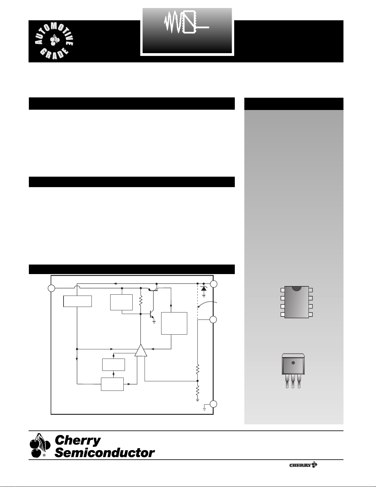
Block Diagram
3L D
2
PAK
Tab (Gnd)
1
1. V
IN
2. Gnd
3. V
OUT
Absolute Maximum Ratings
Power Dissipation . . . . . . . . . . . . . . . . . . . . . . . . . . . . . . . . .Internally Limited
Transient Peak Voltage (60V Load Dump) . . . . . . . . . . . . . . . . . . . .-15V, 74V
Output Current . . . . . . . . . . . . . . . . . . . . . . . . . . . . . . . . . . . .Internally Limited
ESD Susceptibility (Human Body Model) . . . . . . . . . . . . . . . . . . . . . . . . . .2kV
Junction Temperature . . . . . . . . . . . . . . . . . . . . . . . . . . . . . . . . .-40¡C to 150¡C
Storage Temperature . . . . . . . . . . . . . . . . . . . . . . . . . . . . . . . . . .-55¡C to 150¡C
Lead Temperature Soldering
Reflow (SMD styles only) . . . . . .60 sec. max above 183¡C, 230¡C peak
V
IN
V
OUT
NC
Sense
Gnd
Gnd
Gnd
Gnd
8L SO Narrow
(Internally Fused Leads)
A Company
¨
Rev. 12/28/98
Consult factory for TO-92.
Cherry Semiconductor Corporation
2000 South County Trail, East Greenwich, RI 02818
Tel: (401)885-3600 Fax: (401)885-5786
Email: info@cherry-semi.com
Web Site: www.cherry-semi.com
V
IN
Current Source
(Circuit Bias)
Over
Voltage
Shutdown
V
OUT
D2PAK
1
* 8 Lead SO Narrow
Thermal
Shutdown
Bandgap
Reference
+ -
Error
Amplifier
Current Limit
Sense
Sense*
Gnd
2
Electrical Characteristics: 6V ² V
IN
² 26V, I
OUT
= 1mA, -40¡ ² TA² 125¡C, -40¡ ² TJ² 150¡C; unless otherwise specified.
PARAMETER TEST CONDITIONS MIN TYP MAX UNIT
CS8221
Package Lead Description
PACKAGE LEAD # LEAD SYMBOL FUNCTION
■ Output Stage
Output Voltage, V
OUT
9V<VIN<16V, 100µA ² I
OUT
² 100mA 4.90 5.00 5.10 V
6V ² VIN² 26V, 100µA ² I
OUT
² 100mA 4.85 5.00 5.15 V
Dropout Voltage (VIN-V
OUT
)I
OUT
= 100mA 400 600 mV
I
OUT
= 100µA 100 150 mV
Load Regulation VIN= 14V 5 50 mV
100µA ² I
OUT
² 100mA
Line Regulation 6V<V<26V 5 50 mV
I
OUT
= 1mA
Quiescent Current, (IQ)I
OUT
= 100µA, VIN= 6V 60 120 µA
I
OUT
² 50mA 4 6 mA
I
OUT
² 100mA 12 20 mA
Ripple Rejection 7V ² VIN² 17V, I
OUT
= 100mA, 60 75 dB
f = 120Hz
Current Limit 125 200 mA
Short Circuit Output Current V
OUT
= 0V 40 125 µA
Thermal Shutdown (Note 1) 150 180 ¡C
Overvoltage Shutdown V
OUT
²1V 303438 V
Reverse Current V
OUT
= 5V, VIN= 0V 100 500 µA
Note 1: This parameter is guaranteed by design, but not parametrically tested in production.
8L SO Narrow 3L
(Internally Fused Leads) D
2
PAK
11VINInput voltage.
23V
OUT
5V, ±2%, 100mA output.
3 Ð NC No connection.
4 Ð Sense Kelvin connection which allows remote sensing of the output
voltage for improved regulation. If remote sensing is not
required, connect to V
OUT
.
5,6,7,8 2 Gnd Ground.
 Loading...