

Cherry Semiconductor CS8191XDWF20, CS8191XNF16, CS8191XDWFR20 Datasheet
1
Features
■ Direct Sensor Input
■ High Output Torque
■ Wide Output Voltage
Range
■ High Impedance Inputs
■ Accurate down to 10V V
CC
■ Fault Protection
Overvoltage
Short Circuit
■ Low Voltage Operation
Package Options
16 Lead PDIP
(internally fused leads)
CS8191
Precision Air-Core Tach/Speedo Driver
with Short Circuit Protection
20 Lead SOIC
(internally fused leads)
1
CP+
2
3
4
5
6
7
8
SQ
OUT
FREQ
IN
NC
Gnd
Gnd
NC
COS+
16
15
14
13
12
11
10
CP-
F/V
OUT
V
REG
NC
Gnd
Gnd
NC
SIN+
9
COS-
SIN-
17
18
V
CC
BIAS
19
20
Description
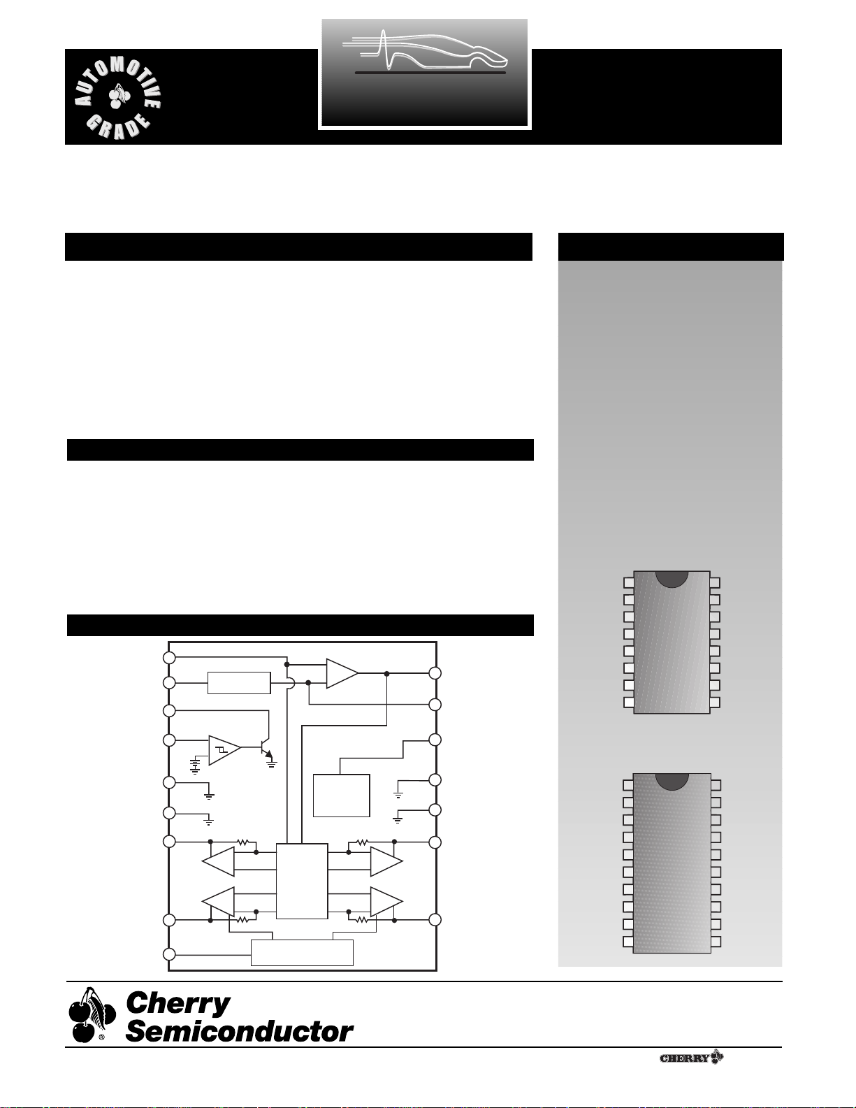
Block Diagram
Absolute Maximum Ratings
The CS8191 is specifically designed
for use with 4 quadrant air-core
meter movements. The IC includes
an input comparator for sensing
input frequency such as vehicle
speed or engine RPM, a charge
pump for frequency to voltage conversion, a bandgap reference for
stable operation and a function
generator with sine and cosine
amplifiers that differentially drive
the motor coils.
The CS8191 has a higher torque
output and better output signal
symmetry than other competitive
parts (CS289, and LM1819). It is
protected against short circuit and
overvoltage (60V) fault conditions.
Enhanced circuitry permits functional operation down to 8V.
CS8191
Supply Voltage ( ² 100ms pulse transient) ...........................................V
CC
= 60V
(continuous)..................................................................V
CC
= 24V
Operating Temperature Range ........................................................-40¡C to +105¡C
Junction Temperature Range ...........................................................-40¡C to +150¡C
Storage Temperature Range.............................................................-55¡C to +165¡C
Electrostatic Discharge (Human Body Model)...................................................4kV
Lead Temperature Soldering
Wave Solder (through hole styles only)..................10 sec. max, 260¡C peak
Reflow (SMD styles only)...................60 sec. max above 183¡C, 230¡C peak
Rev 3/9/99
Cherry Semiconductor Corporation
2000 South County Trail, East Greenwich, RI 02818
Tel: (401)885-3600 Fax: (401)885-5786
Email: info@cherry-semi.com
Web Site: www.cherry-semi.com
A Company
¨
BIAS
SQ
FREQ
CP+
OUT
IN
Charge Pump
Input
Comp.
+
Ð
+
Ð
Voltage
Regulator
F/V
CP-
V
OUT
REG
V
1
CC
V
2
REG
BIAS
3
4
Gnd
5
Gnd
COS-
6
SINE-
7
FREQ
8
IN
16
15
14
13
12
11
10
9
F/V
CP+
CP-
Gnd
Gnd
COS+
SINE+
SQ
OUT
OUT
Gnd
Gnd
COS
COS
V
V
REG
7.0V
+
COS
Output
-
CC
Ð
+
+
Ð
High Voltage, Short
Circuit Protection
Function
Generator
Ð
+
SINE
Output
+
Ð
Gnd
Gnd
SINE+
SINE-
2
Electrical Characteristics: -40¡C ² TA² 105¡C, 8V ² VCC² 16V unless otherwise specified.
PARAMETER TEST CONDITIONS MIN TYP MAX UNIT
CS8191
■ Supply Voltage Section
ICCSupply Current VCC= 16V, -40¡C, No Load 70 125 mA
VCCNormal Operation Range
8.0 13.1 16.0 V
■ Input Comparator Section
Positive Input Threshold 2.4 2.7 3.0 V
Negative Input Threshold 2.0 2.3 V
Input Hysteresis 200 400 1000 mV
Input Bias Current * 0V ² VIN² 8V -2 ±10 µA
Input Frequency Range 0 20 kHz
Input Voltage Range in series with 1k½ -1 V
CC
V
Output V
SAT
ICC= 10mA 0.15 0.40 V
Output Leakage V
CC
= 7V 10 µA
Logic 0 Input Voltage 2.0 V
*Note: Input is clamped by an internal 12V Zener.
■ Voltage Regulator Section
Output Voltage 6.50 7.00 7.50 V
Output Load Current 10 mA
Output Load Regulation 0 to 10 mA 10 50 mV
Output Line Regulation 8.0V ² VCC² 16V 20 150 mV
Power Supply Rejection VCC= 13.1V, 1VP/P1kHz 34 46 dB
■ Charge Pump Section
Inverting Input Voltage 1.5 2.0 2.5 V
Input Bias Current 40 150 nA
V
BIAS
Input Voltage 1.5 2.0 2.5 V
Non Invert. Input Voltage IIN= 1mA 0.7 1.1 V
Linearity* @ 0, 87.5, 175, 262.5, + 350Hz -0.10 0.28 +0.70 %
F/V
OUT
Gain @ 350Hz, CT= 0.0033µF, RT= 243k½ 7 10 13 mV/Hz
Norton Gain, Positive IIN= 15µA 0.9 1.0 1.1 I/I
Norton Gain, Negative IIN= -15µA 0.9 1.0 1.1 I/I
*Note: Applies to % of full scale (270¡).
■ Function Generator Section: -40¡ ² T
A
² 85¡C, VCC= 13.1V unless otherwise noted.
Differential Drive Voltage 10V ² VCC² 16V 7.5 8.0 8.5 V
(V
COS
+ - V
COS
-) Q = 0¡
Differential Drive Voltage 10V ² VCC² 16V 7.5 8.0 8.5 V
(V
SIN
+ - V
SIN
-) Q = 90¡
Differential Drive Voltage 10V ² VCC² 16V -8.5 -8.0 -7.5 V
(V
COS
+ - V
COS
-) Q = 180¡
Differential Drive Voltage 10V ² VCC² 16V -8.5 -8.0 -7.5 V
(V
SIN
+ - V
SIN
-) Q = 270¡
Differential Drive Load 10V ² VCC² 16V, -40¡C 178 ½
25¡C 239 ½
105¡C 314 ½
Zero Hertz Output Voltage -0.08 0.0 +0.08 V
3
PACKAGE LEAD # LEAD SYMBOL FUNCTION
CS8191
Electrical Characteristics:
continued
PARAMETER TEST CONDITIONS MIN TYP MAX UNIT
Package Lead Description
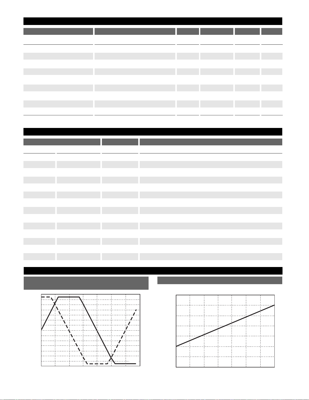
Typical Performance Characteristics
0 45 90 135 180 225 270 315
Output Voltage (V)
Degrees of Deflection (°)
7
6
5
4
3
2
1
0
-1
-2
-3
-4
-5
-6
-7
COS
SIN
045
90
135 180 225 270 315
F/V Output (V)
Frequency/Output Angle (°)
7
6
5
4
3
2
1
0
Figure 2: Charge Pump Output Voltage vs Output Angle
Figure 1: Function Generator Output Voltage
vs Degrees of Deflection
F/V
OUT
= 2.0V + 2 FREQ ´ CT´ RT´ (V
REG
- 0.7)
■ Function Generator Section: continued
Function Generator Error * Q = 0¡ to 225¡ -2 0 +2 deg
Reference Figures 1 - 4 Q = 226¡ to 305¡ -3 0 +3 deg
Function Generator Error 13.1V ² V
CC
² 16V -1 0 +1 deg
Function Generator Error 13.1V ² V
CC
² 10V -1 0 +1 deg
Function Generator Error 13.1V ² V
CC
² 8.0V -7 0 +7 deg
Function Generator Error 25¡C ² T
A
² 80¡C -2 0 +2 deg
Function Generator Error 25¡C ² T
A
² 105¡C -4 0 +4 deg
Function Generator Error Ð40¡C ² T
A
² 25¡C -2 0 +2 deg
Function Generator Gain T
A
= 25¡C, Q vs F/V
OUT
60 77 95 ¡/V
*Note: Deviation from nominal per Table 1 after calibration at 0¡ and 270¡.
16L PDIP 20L SO
11VCCIgnition or battery supply voltage.
22V
REG
Voltage regulator output.
3 3 BIAS Test point or zero adjustment.
4, 5, 12, 13 5, 6, 15, 16 Gnd Ground Connections.
6 8 COS- Negative cosine output signal.
7 9 SIN- Negative sine output signal.
8 10 FREQ
IN
Speed or rpm input signal.
911SQ
OUT
Buffered square wave output signal.
10 12 SIN+ Positive sine output signal.
11 13 COS+ Positive cosine output signal.
14 18 CP- Negative input to charge pump.
15 19 CP+ Positive input to charge pump.
16 20 F/V
OUT
Output voltage proportional to input signal frequency.
4, 7, 14, 17 NC No connection.
 Loading...