

Cherry Semiconductor CS8190EDWFR20 Datasheet
1
Features
■
Direct Sensor Input
■
High Output Torque
■
Low Pointer Flutter
■
High Input Impedance
■ Overvoltage Protection
■ Return to Zero
Package Options
16 Lead PDIP
(internally fused leads)
20 Lead SOIC
(internally fused leads)
CS8190
Precision Air-Core Tach/Speedo Driver
with Return to Zero
1
CP+
2
3
4
5
6
7
8
SQ
OUT
FREQ
IN
Gnd
Gnd
COS+
16
15
14
13
12
11
10
CP-
F/V
OUT
V
REG
Gnd
Gnd
SIN+
9
COS- SIN-
17
18
V
CC
BIAS
19
20
Gnd
Gnd
Gnd
Gnd
CS8190
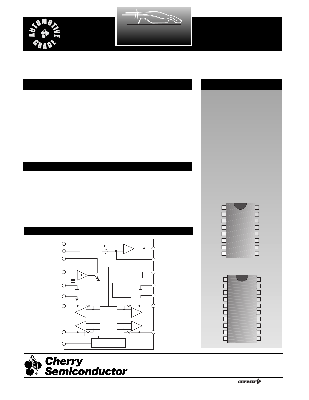
Description
The CS8190 is specifically designed
for use with air-core meter movements. The IC provides all the functions necessary for an analog
tachometer or speedometer. The
CS8190 takes a speed sensor input
and generates sine and cosine related output signals to differentially
drive an air-core meter.
Many enhancements have been
added over industry standard
tachometer drivers such as the
CS289 or LM1819. The output utilizes differential drivers which eliminates the need for a zener reference
and offers more torque. The device
withstands 60V transients which
decreases the protection circuitry
required. The device is also more
precise than existing devices allowing for fewer trims and for use in a
speedometer.
Block Diagram
Absolute Maximum Ratings
Supply Voltage (<100ms pulse transient) .........................................VCC= 60V
(continuous)..............................................................VCC= 24V
Operating Temperature .............................................................Ð40¡C to +105¡C
Storage Temperature..................................................................Ð40¡C to +165¡C
Junction Temperature .................................................................Ð40¡C to+150¡C
ESD (Human Body Model) .............................................................................4kV
Lead Temperature Soldering
Wave Solder(through hole styles only).............10 sec. max, 260¡C peak
Reflow (SMD styles only).............60 sec. max above 183¡C, 230¡C peak
A Company
¨
Rev. 11/21/96
Cherry Semiconductor Corporation
2000 South County Trail, East Greenwich, RI 02818
Tel: (401)885-3600 Fax: (401)885-5786
Email: info@cherry-semi.com
Web Site: www.cherry-semi.com
BIAS
SQ
FREQ
CP+
OUT
IN
Gnd
Gnd
Charge Pump
Input
Comp.
+
Ð
Voltage
Regulator
V
REG
7.0V
+
Ð
F/V
CP-
V
Gnd
Gnd
OUT
REG
1
CP+
2
SQ
OUT
Gnd
Gnd
COS+
COS-
V
3
IN
4
5
6
7
8
CC
FREQ
16
15
14
13
12
11
10
9
CP-
F/V
V
REG
Gnd
Gnd
SINE+
SINE-
BIAS
OUT
COS
COS
+
Output
-
V
CC
COS
Ð
+
+
Ð
Func.
Gen.
High Voltage
Protection
Ð
+
SINE
Output
+
Ð
SINE+
SINE-
2
Electrical Characteristics:
-40¡C ² TA² 85¡C, 8.5V ² VCC² 15V unless otherwise specified.
PARAMETER TEST CONDITIONS MIN TYP MAX UNIT
CS8190
■ Supply Voltage Section
I
CC
Supply Current VCC= 16V, -40¡C, No Load 50 125 mA
VCCNormal Operation Range
8.5 13.1 16.0 V
■ Input Comparator Section
Positive Input Threshold 1.0 2.0 3.0 V
Input Hysteresis 200 500 mV
Input Bias Current * 0V ² V
IN
² 8V -10 -80 µA
Input Frequency Range 0 20 KHz
Input Voltage Range in series with 1k½ -1 V
CC
V
Output V
SAT
ICC= 10mA 0.15 0.40 V
Output Leakage V
CC
= 7V 10 µA
Low V
CC
Disable Threshold 7.0 8.0 8.5 V
Logic 0 Input Voltage 1 V
* Note: Input is clamped by an internal 12V Zener.
■ Voltage Regulator Section
Output Voltage 6.25 7.00 7.50 V
Output Load Current 10 mA
Output Load Regulation 0 to 10 mA 10 50 mV
Output Line Regulation 8.5V ² V
CC
² 16V 20 150 mV
Power Supply Rejection V
CC
= 13.1V, 1Vp/p 1kHz 34 46 dB
■ Charge Pump Section
Inverting Input Voltage 1.5 2.0 2.5 V
Input Bias Current 40 150 nA
V
BIAS
Input Voltage 1.5 2.0 2.5 V
Non Invert. Input Voltage I
IN
= 1mA 0.7 1.1 V
Linearity* @ 0, 87.5, 175, 262.5, + 350Hz -0.10 0.28 +0.70 %
F/V
OUT
Gain @ 350Hz, CT= 0.0033µF, RT= 243k½ 7 10 13 mV/Hz
Norton Gain, Positive I
IN
= 15µA 0.9 1.0 1.1 I/I
Norton Gain, Negative I
IN
= 15µA 0.9 1.0 1.1 I/I
* Note: Applies to % of full scale (270¡)
■ Function Generator Section: -40¡ ² T
A
² 85¡C, VCC= 13.1V unless otherwise noted.
Return to Zero Threshold T
A
= 25¡C 5.2 6.0 7.0 V
Differential Drive Voltage 8.5V ² V
CC
² 16V 5.5 6.5 7.5 V
(V
COS
+ - V
COS
-) Q = 0¡
Differential Drive Voltage 8.5V ² V
CC
² 16V 5.5 6.5 7.5 V
(V
SIN
+ - V
SIN
-) Q = 90¡
Differential Drive Voltage 8.5V ² V
CC
² 16V -7.5 -6.5 -5.5 V
(V
COS
+ - V
COS
-) Q = 180¡
Differential Drive Voltage 8.5V ² V
CC
² 16V -7.5 -6.5 -5.5 V
(V
SIN
+ - V
SIN
-) Q = 270¡
Differential Drive Current 8.5V ² V
CC
² 16V 33 42 mA
Zero Hertz Output Angle -1.5 0.0 1.5 deg
3
PACKAGE LEAD # LEAD SYMBOL FUNCTION
CS8190
Electrical Characteristics:
continued
PARAMETER TEST CONDITIONS MIN TYP MAX UNIT
Package Lead Description
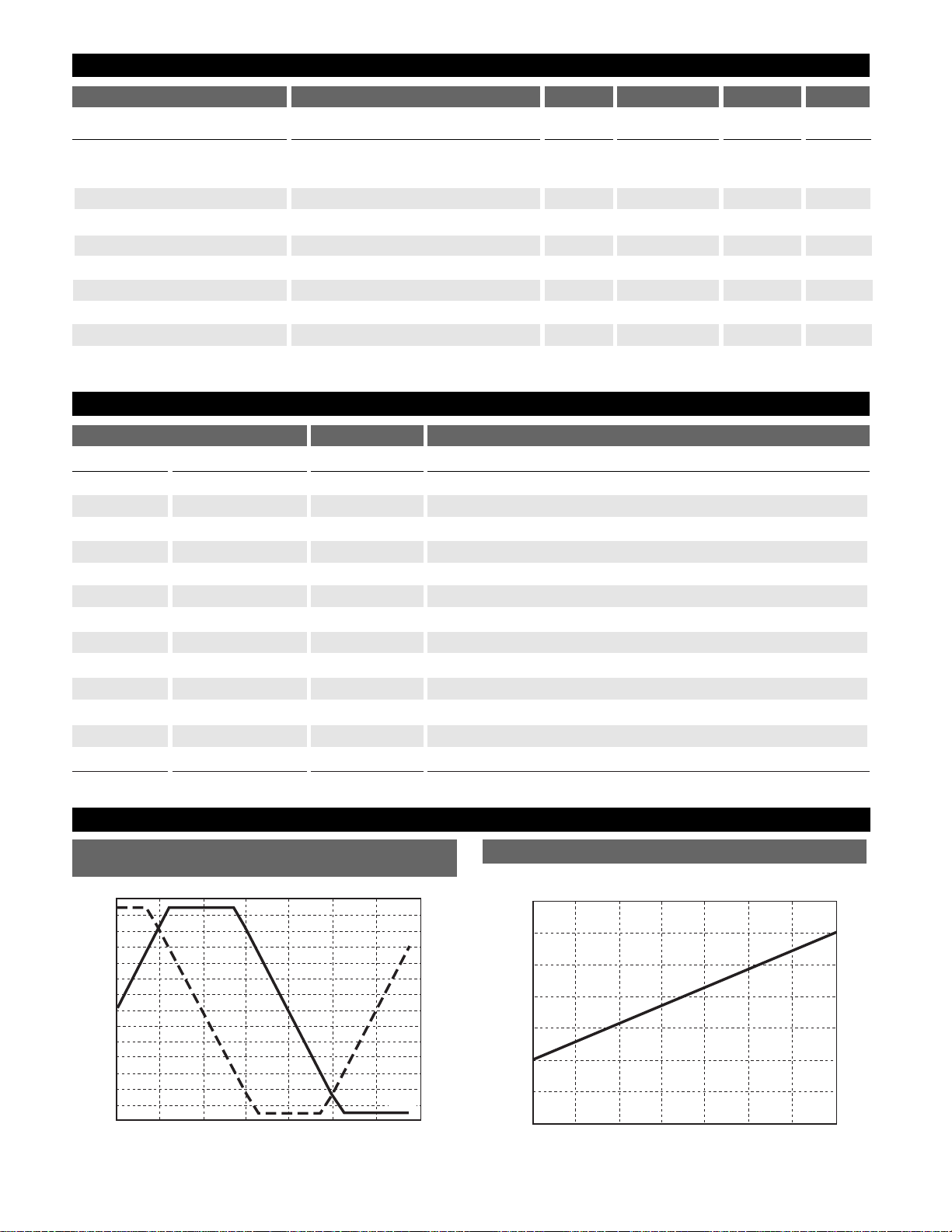
Typical Performance Characteristics
0 45 90 135 180 225 270 315
Output Voltage (V)
Degrees of Deflection (°)
7
6
5
4
3
2
1
0
-1
-2
-3
-4
-5
-6
-7
COS
SIN
045
90
135 180 225 270 315
F/V Output (V)
Frequency/Output Angle (°)
7
6
5
4
3
2
1
0
Figure 2: Charge Pump Output Voltage vs Output Angle
Figure 1: Function Generator Output Voltage
vs Degrees of Deflection
F/V
OUT
= 2.0V + 2 FREQ ´ CT´ RT´ (V
REG
- 0.7V)
■ Function Generator Section: continued
Function Generator Error * V
CC
= 13.1V -2 0 +2 deg
Reference Figures 1 - 4 Q = 0¡ to 305¡
Function Generator Error 13.1V ² V
CC
² 16V -2.5 0 +2.5 deg
Function Generator Error 13.1V ² V
CC
² 11V -1 0 +1 deg
Function Generator Error 13.1V ² V
CC
² 9V -3 0 +3 deg
Function Generator Error 25¡C ² T
A
² 80¡C -3 0 +3 deg
Function Generator Error 25¡C ² T
A
² 105¡C -5.5 0 +5.5 deg
Function Generator Error Ð40¡C ² T
A
² 25¡C -3 0 +3 deg
Function Generator Gain T
A
= 25¡C, Q vs F/V
OUT
60 77 95 ¡/V
* Note: Deviation from nominal per Table 1 after calibration at 0 and 270¡.
16L 20L
1 1 CP+ Positive input to charge pump.
22SQ
OUT
Buffered square wave output signal.
3 3 FREQ
IN
Speed or rpm input signal.
4, 5, 12, 13 4 - 7, 14 - 17 Gnd Ground Connections.
6 8 COS+ Positive cosine output signal.
7 9 COS- Negative cosine output signal.
810VCCIgnition or battery supply voltage.
9 11 BIAS Test point or zero adjustment.
10 12 SIN- Negative sine output signal.
11 13 SIN+ Positive sine output signal.
14 18 V
REG
Voltage regulator output.
15 19 F/V
OUT
Output voltage proportional to input signal frequency.
16 20 CP- Negative input to charge pump.
 Loading...