

Cherry Semiconductor CS8164YTVA5, CS8164YTHA5, CS8164YT5 Datasheet
1
Features
■ Two Regulated Outputs
Primary Output
8V ±5%; 750mA
Secondary Output
5V ±2%; 100mA
■ Low Dropout Voltage
■ ON/OFF Control
Option
■ Standby Quiescent Drain
(<2mA)
■ Protection Features
Reverse Battery
60V Peak Transient
Voltage
-50V Reverse Transient
Short Circuit
Thermal Shutdown
Package Options
5 Lead TO-220
Tab (Gnd)
1
CS8164
8V/5V Low Dropout Dual Regulator
with ENABLE
CS8164
Description
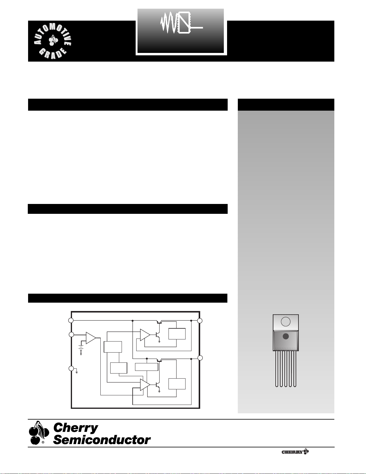
Block Diagram
Absolute Maximum Ratings
DC Input Voltage.............................................................................-0.5V to 26V
Transient Peak Voltage (46V Load Dump).................................................60V
Internal Power Dissipation..................................................Internally Limited
Operating Temperature Range................................................-40¡C to +125¡C
Junction Temperature Range...................................................-40¡C to +150¡C
Storage Temperature Range ....................................................-65¡C to +150¡C
Reverse Polarity V
OUT1
Input Voltage, DC ................................................-18V
Reverse Polarity Input Voltage, Transient ................................................-50V
Lead Temperature Soldering
Wave Solder (through hole styles only)..........10 sec. max, 260¡C peak
The CS8164 is a low dropout, dual
8V/5V linear regulator. The secondary
5V/100mA output is used for powering
systems with standby memory.
Quiescent current drain is less than
2mA when supplying 10mA loads from
the standby regulator.
In automotive applications, the CS8164
and all regulated circuits are protected
from reverse battery installations, as
well as high voltage transients. During
line transients, such as a 60V load
dump, the 750mA output will automat-
ically shutdown to protect both internal
circuits and the load, while the secondary regulator continues to power
any standby load.
The on board ENABLE function controls the regulator's primary output.
When ENABLE is in the low state, the
regulator is placed in STANDBY mode
where it draws 2mA (typ) quiescent
current.
The CS8164 is packaged in a 5-lead
TO-220, with copper tab for connection
to a heat sink, if necessary.
1V
IN
2V
OUT1
3 Gnd
4 ENABLE
5V
OUT2
A Company
¨
Rev. 2/17/98
Cherry Semiconductor Corporation
2000 South County Trail, East Greenwich, RI 02818
Tel: (401)885-3600 Fax: (401)885-5786
Email: info@cherry-semi.com
Web Site: www.cherry-semi.com
V
ENABLE
Gnd
IN
+
Bandgap
Reference
Thermal
Shutdown
Standby Output
+
-
Primary Output
Over Voltage
Shutdown
+
-
Output
Current
Limit
Output
Current
Limit
V
V
OUT2
OUT1
2
CS8164
PARAMETER TEST CONDITIONS MIN TYP MAX UNIT
Electrical Characteristics for V
OUT
: VIN= 14V, I
OUT
= 500mA, -40¡C ² TJ² +150ûC unless otherwise specified
Package Lead Description
PACKAGE LEAD # LEAD SYMBOL FUNCTION
5 Lead TO-220
1V
IN
Supply voltage, usually direct from battery.
2V
OUT1
Regulated output 8V, 750mA (typ).
3 Gnd Ground connection.
4 ENABLE CMOS compatible input lead; switches V
OUT1
on and off. When
ENABLE is high, V
OUT1
is active.
5V
OUT2
Standby output 5V, 100mA (typ); always on.
■ OUTPUT STAGE (V
OUT1
)
Output Voltage, V
OUT1
13V ² VIN² 26V, I
OUT1
² 500mA, 7.6 8.0 8.4 V
13V ² VIN² 16V, I
OUT1
² 750mA 7.6 8.0 8.4 V
Dropout Voltage I
OUT1
= 500mA 0.60 V
Line Regulation 13V ² VIN² 16V, I
OUT1
= 5mA 15 80 mV
Load Regulation 5mA ² I
OUT1
² 500mA 15 80 mV
Quiescent Current I
OUT1
² 10mA, No Load on Standby 3 7 mA
I
OUT1
= 500mA, No Load on Standby 40 100 mA
I
OUT1
= 750mA, No Load on Standby 90 mA
Ripple Rejection f = 120Hz 53 dB
Current Limit 0.75 1.40 2.50 A
Long Term Stability 50 mV/khr
Output Impedance 500mA DC and 10mA rms, 200 m½
100Hz - 10kHz
Thermal Shutdown 150 190 ¡C
Overvoltage Shutdown 26 40 V
■ Standby Output (V
OUT2
)
Output Voltage, (V
OUT2
) 6V ² VIN² 26V 4.75 5.00 5.25 V
Dropout Voltage I
OUT2
² 100mA 0.55 0.70 V
Line Regulation 6V ² VIN² 26V 4 50 mV
Load Regulation 1mA ² I
OUT2
² 100mA 10 50 mV
Quiescent Current I
OUT2
² 10mA, -40ûC ² TJ² +125ûC 2 3 mA
V
OUT1
OFF
Ripple Rejection f = 120Hz 66 dB
Current Limit 200 mA
Long Term Stability 20 mV/khr
Output Impedance 10mA DC and 1mA rms, 100Hz - 10kHz 1 ½
■ ENABLE Function (ENABLE)
Input ENABLE Threshold V
OUT1
Off 1.25 0.80 V
V
OUT1
On 2.00 1.25 V
Input ENABLE Current V
ENABLE²VTHRESHOLD
-10 10 µA
3
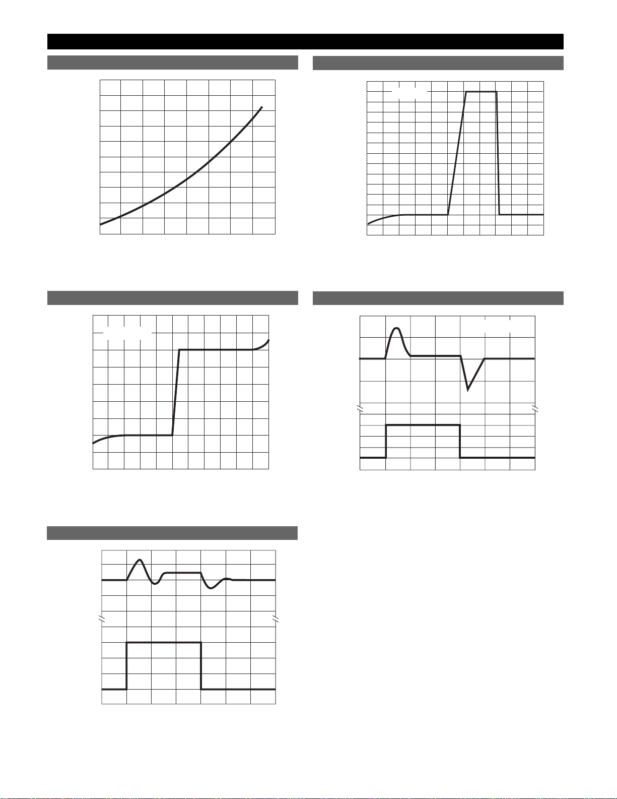
Typical Performance Characteristics
CS8164
1.0
0.9
0.8
0.7
0.6
0.5
0.4
0.3
0.2
0.1
0.0
INPUT-OUTPUT DIFFERENTIAL VOLTAGE (V)
OUTPUT CURRENT (mA)
0 200 400 600 800
Dropout Voltage vs. Output Current
7
6
5
4
3
2
1
0
-1
-2
INPUT VOLTAGE (V)
OUTPUT VOLTAGE (V)
8
9
10
11
12
13
-40 -20 0 20 40 60
RL=10W
Output Voltage vs. Input Voltage
7
6
5
4
3
2
1
0
-1
-2
INPUT VOLTAGE (V)
OUTPUT VOLTAGE (V)
-40 -20 0 20 40 60
RL= 500W
Standby Output Voltage vs. Input Voltage
20
10
0
-10
-20
3
2
1
0
TIME (ms)
INPUT VOLTAGE
CHANGE (V)
OUTPUT VOLTAGE
DEVIATION (mV)
I
OUT1
= 500mA
0 102030405060
Line Transient Response (V
OUT1
)
10
TIME (ms)
INPUT VOLTAGE
CHANGE (V)
OUTPUT VOLTAGE
DEVIATION (mV)
5
0
-5
-10
3
2
1
0
0 1020 3040 5060
Line Transient Response (V
OUT2
)
 Loading...