

Cherry Semiconductor CS8156YTVA5, CS8156YTHA5, CS8156YT5 Datasheet
1
Features
■ Two regulated outputs
12V ±5.0%; 750mA
5V ±2.0%; 100mA
■ Very low SLEEP mode
current drain 200nA
■ Fault Protection
Reverse Battery
+60V, -50V Peak
Transient Voltage
Short Circuit
Thermal Shutdown
■ CMOS Compatible
ENABLE
Package Options
5 Lead TO-220
Tab (Gnd)
1
CS8156
12V, 5V Low Dropout Dual Regulator
with ENABLE
CS8156
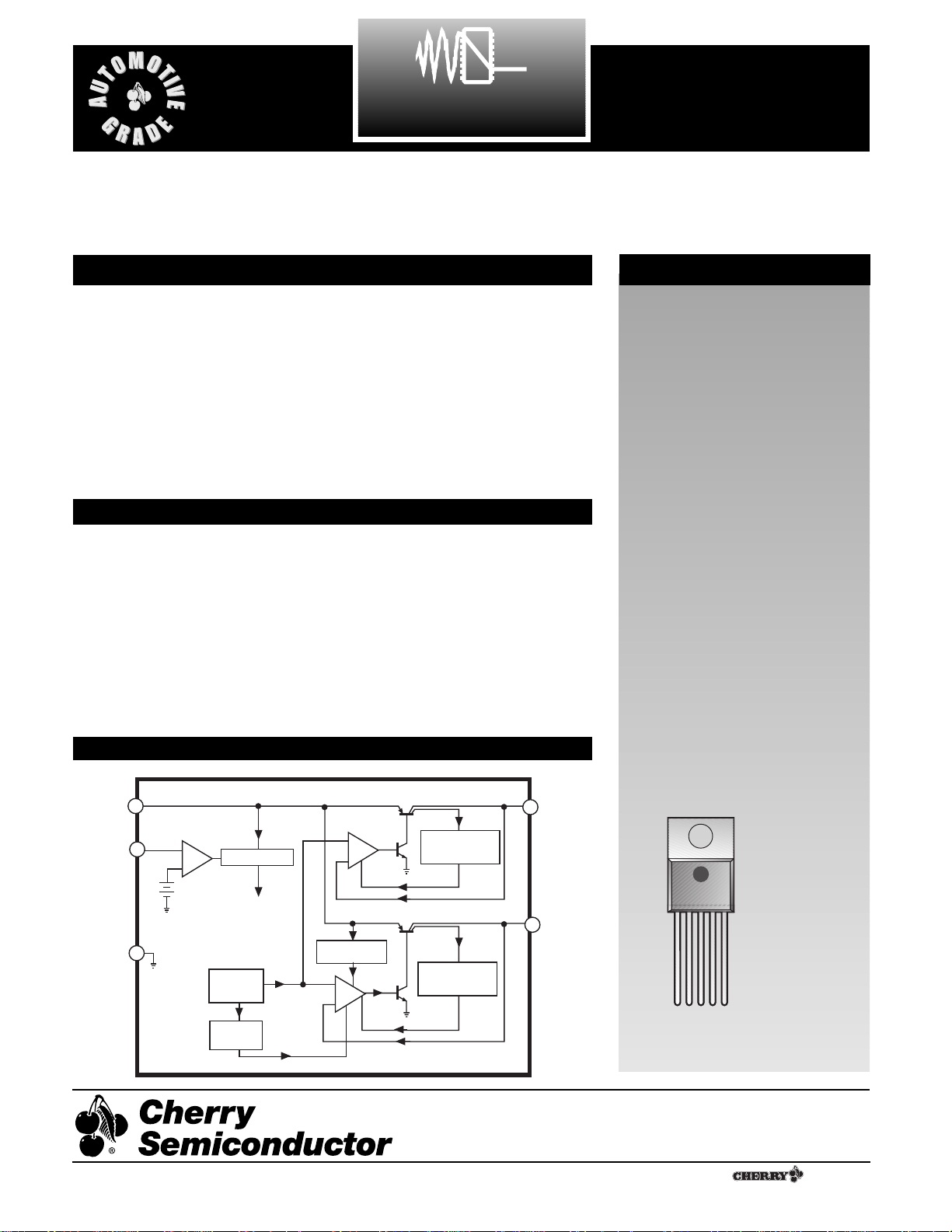
Description
V
IN
V
OUT
2
, 5V
Gnd
V
OUT
1
, 12V
ENABLE
+
-
Bandgap
Reference
+
-
+
-
Thermal
Shutdown
Over Voltage
Shutdown
Anti-Saturation
and
Current Limit
Anti-Saturation
and
Current Limit
Pre-Regulator
Block Diagram
Absolute Maximum Ratings
Input Voltage
Operating Range.....................................................................-0.5V to 26V
Peak Transient Voltage (Load Dump = 46V) ....................................60V
Internal Power Dissipation..................................................Internally Limited
Operating Temperature Range................................................-40¡C to +125¡C
Junction Temperature Range...................................................-40¡C to +150¡C
Storage Temperature Range ....................................................-65¡C to +150¡C
Lead Temperature Soldering
Wave Solder (through hole styles only)..........10 sec. max, 260¡C peak
The CS8156 is a low dropout 12V/5V
dual output linear regulator. The 12V
± 5% output sources 750mA and the 5V
±2.0% output sources 100mA.
The on board ENABLE function controls the regulatorÕs two outputs. When
the ENABLE lead is low, the regulator
is placed in SLEEP mode. Both outputs
are disabled and the regulator draws
only 200nA of quiescent current.
The regulator is protected against overvoltage conditions. Both outputs are
protected against short circuit and thermal runaway conditions.
The CS8156 is packaged in a 5 lead
TOÐ220 with copper tab. The copper
tab can be connected to a heat sink if
necessary.
1V
I
N
2V
OUT1
3 Gnd
4 ENABLE
5V
OUT2
A Company
¨
Rev. 2/19/98
Cherry Semiconductor Corporation
2000 South County Trail, East Greenwich, RI 02818
Tel: (401)885-3600 Fax: (401)885-5786
Email: info@cherry-semi.com
Web Site: www.cherry-semi.com
2
CS8156
PARAMETER TEST CONDITIONS MIN TYP MAX UNIT
Package Lead Description
PACKAGE LEAD # LEAD SYMBOL FUNCTION
5 Lead TO-220
1V
IN
Supply voltage, usually direct from battery.
2V
OUT1
Regulated output 12V, 750mA (typ)
3 Gnd Ground connection.
4 ENABLE CMOS compatible input lead; switches outputs on and off.
When ENABLE is high V
OUT1
and V
OUT2
are active.
5V
OUT2
Regulated output 5V, 100mA (typ).
Electrical Characteristics for V
OUT
: VIN= 14.5V, I
OUT1
= 5mA, I
OUT2
= 5mA, -40¡C ² TJ² +150ûC, -40¡C ² T
C
² +125ûC
unless otherwise specified
■ Output Stage(V
OUT1
)
Output Voltage, V
OUT1
13V ² V
IN
² 16V, I
OUT1
² 750mA 11.2 12.0 12.8 V
Dropout Voltage I
OUT1
= 500mA 0.4 0.6 V
I
OUT1
= 750mA 0.6 1.0 V
Line Regulation 13V ² V
IN
² 16V ,5mA ² I
OUT
< 100mA 15 80 mV
Load Regulation 5mA ² I
OUT1
² 500mA 15 80 mV
Quiescent Current I
OUT1
² 500mA, No Load on Standby 45 125 mA
I
OUT1
² 750mA, No Load on Standby 100 250 mA
Sleep Mode ENABLE = Low 200 nA
Ripple Rejection f = 120Hz, I
OUT
= 5mA, 42 70 dB
V
IN
= 1.5VPPat 15.5V
DC
Current Limit 0.75 1.20 2.50 A
Maximum Line Transient V
OUT1
² 13V 60 90 V
Reverse Polarity V
OUT1
³ -0.6V, 10½ Load -18 -30 V
Input Voltage, DC
Reverse Polarity Input 1% Duty Cycle, t = 100ms, V
OUT
³ -6V, -50 -80 V
Voltage, Transient 10½ Load
Output Noise Voltage 10Hz - 100kHz 500 µVrms
Output Impedance 500mA DC and 10mA rms, 100Hz 0.2 1.0 ½
Over-voltage Shutdown 28 34 45 V
■ Standby Output (V
OUT2
)
Output Voltage, (V
OUT2
) 9V ² V
IN
² 16V, 1mA ² I
OUT2
² 100mA 4.90 5.00 5.10 V
Dropout Voltage I
OUT2
² 100mA 0.60 V
Line Regulation 6V ² V
IN
² 26V; 1mA ² I
OUT
² 100mA 5 50 mV
Load Regulation 1mA ² I
OUT2
² 100mA; 9V ² V
IN
² 16V 5 50 mV
Quiescent Current V
OUT1
OFF, V
OUT2
OFF, V
ENABLE
= 0.8V 1 350 µA
Ripple Rejection f = 120Hz; I
OUT
= 100mA, 42 70 dB
V
IN
= 1.5VPPat 14.5V
DC
Current Limit 100 200 mA
■ ENABLE Function (ENABLE)
Input ENABLE Threshold V
OUT1
Off 1.25 0.80 V
V
OUT1
On 2.00 1.25 V
Input ENABLE Current V
ENABLE ²VTHRESHOLD
-10 0 10 µA
3
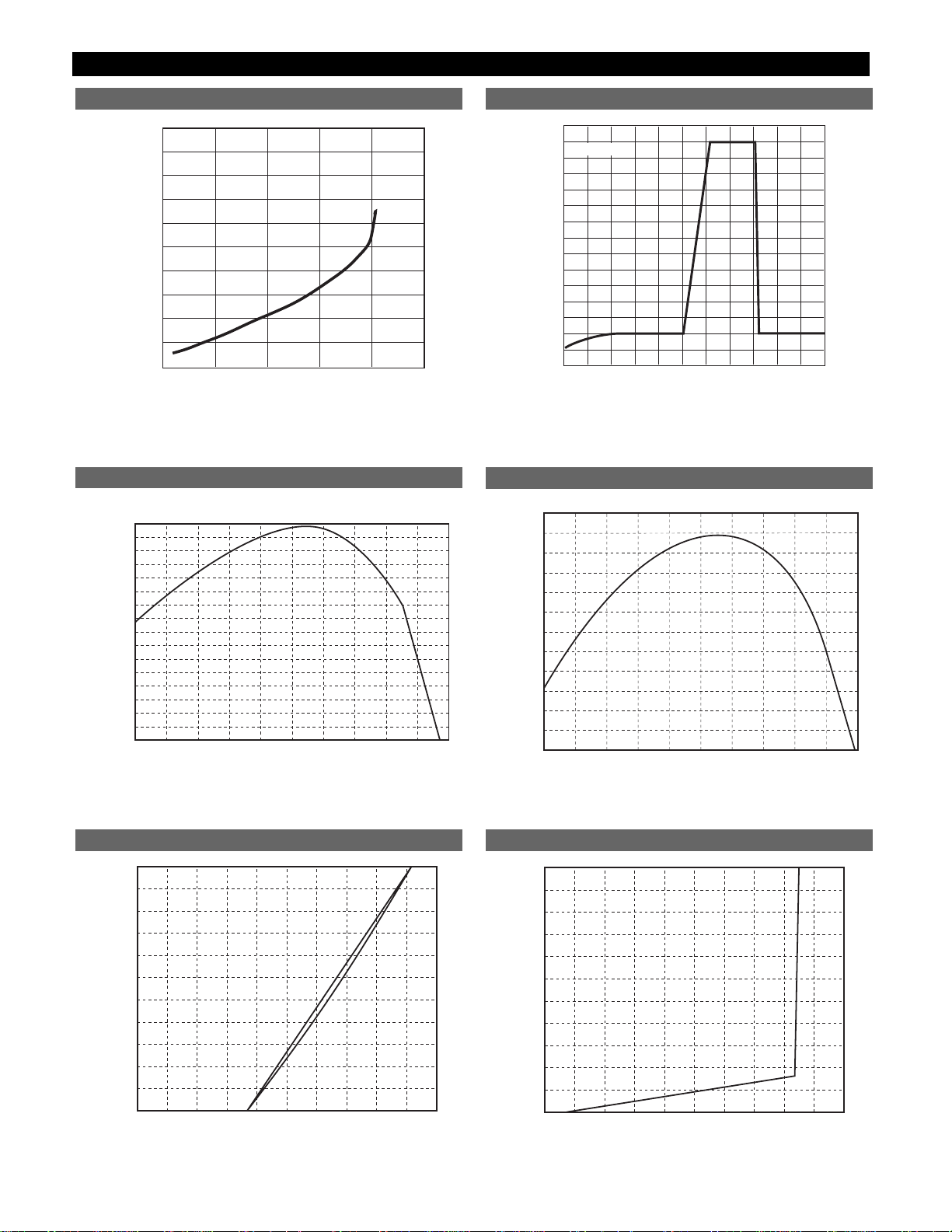
Typical Performance Characteristics
CS8156
0
0
50 100 150 200
Dropout Voltage (mV)
I
OUT
(mA)
200
400
600
800
1000
1200
1400
1600
1800
2000
Dropout Voltage vs I
OUT2
INPUT VOLTAGE (V)
OUTPUT VOLTAGE (V)
7
6
5
4
3
2
1
0
-1
-2
-40 -20 0 20 40 60
8
9
10
11
12
13
RL=10W
V
OUT1
vs. Input Voltage
-20
Temp (°C)
V
OUT
1
(V)
11.75
12.15
0 20 40 60 80 100 120 140 160-40
12.10
12.05
12.00
11.95
11.90
11.85
11.80
V
OUT1
vs. Temperature
-20
5.020
Temp (°C)
V
OUT
2
(V)
5.010
5.000
4.990
4.980
4.970
5.030
0 20 40 60 80 100 120 140 160-40
V
OUT2
vs. Temperature
V
ENABLE
(V)
I
ENABLE
(mA)
0
0
100
5
1234
20
40
60
80
ENABLE Current vs. ENABLE Voltage
V
ENABLE
(V)
I
ENABLE
(mA)
0.0
0.0
5.0
25
4.0
3.0
2.0
1.0
5101520
ENABLE Current vs. ENABLE Voltage
 Loading...