

Cherry Semiconductor CS8141YTVA7, CS8141YTHA7, CS8141YT7, CS8141YN14, CS8141YDWF24 Datasheet
...
The CS8140 is a 5V Watchdog
Regulator with protection circuitry and
three logic control functions that allow
a microprocessor to control its own
power supply. The CS8140 is designed
for use in automotive, switch mode
power supply post regulator, and battery powered systems.
Basic regulator performance characteristics include a low noise, low drift, 5V
± 4% precision output voltage with low
dropout voltage (1.25V @ I
OUT
= 500mA)
and low quiescent current (7mA @ I
OUT
= 500mA). On board short circuit, thermal, and overvoltage protection make it
possible to use this regulator in particularly harsh operating environments.
The Watchdog logic function monitors
an input signal (WDI) from the microprocessor or other signal source. When
the signal frequency moves outside
externally programmable window limits, a signal is generated
( ). An external capacitor
(C
DELAY
) programs the watchdog window frequency limits as well as the
power on reset (POR) and delay.
The function is activated by any
of three conditions: the watchdog signal moves outside of its preset limits;
the output voltage drops out of regulation by more than 4.5%; or the IC is in
its power up sequence. The signal is independent of V
IN
and reliable
down to V
OUT
= 1V.
In conjunction with the Watchdog, the
ENABLE function controls the regulatorÕs power consumption. The CS8140Õs
output stage and its attendant circuitry
are enabled by setting the ENABLE
lead high. The regulator goes into sleep
mode (I
OUT
= 250µA) when the
ENABLE lead goes low and the watchdog signal moves outside its preset
window limits. This unique combination of control functions in the CS8140
gives the microprocessor control over
its own power down sequence: i.e. it
gives the microprocessor the flexibility
to perform housekeeping functions
before it powers down.
The CS8141 has the same features as the
CS8140, except that the CS8141 only
responds to input signals (WDI) which
are below the preset watchdog frequency threshold.
RESET
RESET
RESET
RESET
RESET
1
Features
■
5V ± 4%, 500mA Output
Voltage
■
µP Compatible Control
Functions
Watchdog
ENABLE
■
Low Dropout Voltage
(1.25V @ 500mA)
■
Low Quiescent Current
(7mA @ 500mA)
■
Low Noise, Low Drift
■
Low Current SLEEP Mode
(I
Q
= 250µA)
■
Fault Protection
Thermal Shutdown
Short Circuit
60V Peak Transient
Voltage
RESET
Package Options
7 Lead TO-220
Tab (Gnd)
14 Lead PDIP
24 Lead SOIC Wide
CS8140/1
5V, 500mA Linear Regulator
with
ENABLE, , and Watchdog
RESET
Delay
V
OUT
Sense
WDI
NC
NC
NC
NC
NC
V
IN
ENABLE
RESET
Gnd
NC
NC
NC
Gnd
NC
NC
NC
NC
NC
NC
NC
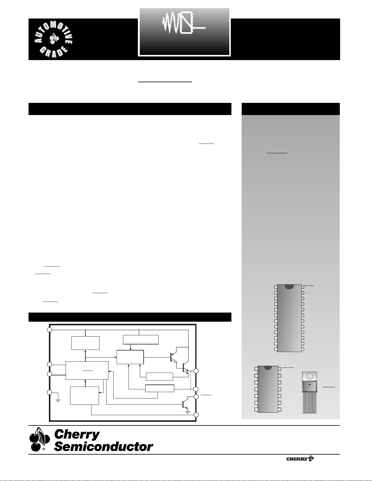
CS8140/1
Description
Block Diagram
Delay
V
OUT
Sense
WDI
NC
NC
NC
NC
NC
Gnd
V
IN
ENABLE
RESET
NC
1V
IN
2 ENABLE
3
4 Gnd
5 Delay
6 WDI
7V
OUT
RESET
A Company
¨
Rev. 2/23/99
Cherry Semiconductor Corporation
2000 South County Trail, East Greenwich, RI 02818
Tel: (401)885-3600 Fax: (401)885-5786
Email: info@cherry-semi.com
Web Site: www.cherry-semi.com
V
IN
Reference
& Bias
Overvoltage
Overtemperature
1
ENABLE
WDI
Gnd
Control Logic
ENABLE
RESET
Delay
Watchdog
Regulation
Short Circuit
Undervoltage
V
OUT
*NOTE: shorted together
*
on 7 Lead TO-220
Sense
RESET
Delay
1
1

2
Electrical Characteristics: 7V ² V
IN
² 26V, 5mA ² I
OUT
² 500mA, -40ûC ² TJ² +150ûC, -40ûC ² TA² 125ûC
unless otherwise specified
PARAMETER TEST CONDITIONS MIN TYP MAX UNIT
Absolute Maximum Ratings
Input Voltage
Operating Range.................................................................................................................................................-0.5 to +26V
Peak Transient Voltage (46V Load Dump @ 14V V
BAT
)..............................................................................................60V
Electrostatic Discharge
(Human Body Model)...............................................................................................................................................4kV
WDI Input Signal Range...............................................................................................................................................-0.3 to +7V
Internal Power Dissipation ..............................................................................................................................Internally limited
Junction Temperature Range (TJ).......................................................................................................................-40¡C to +150¡C
Storage Temperature Range................................................................................................................................-65¡C to +150¡C
Lead Temperature Soldering
Wave Solder (through hole styles only) .....................................................................................10 sec. max, 260¡C peak
Reflow (SMD styles only) ......................................................................................60 sec. max above 183¡C, 230¡C peak
ENABLE .......................................................................................................................................................................-0.3V to V
IN
CS8140/1
■ Output Stage (V
OUT
)
Output Voltage, V
OUT
7V ² VIN² 26V 4.8 5.0 5.2 V
5mA < I
OUT
< 500mA
Dropout Voltage (VIN- V
OUT
)I
OUT
= 500mA 1.25 1.50 V
Line Regulation I
OUT
= 50mA, 5 25 mV
7V ² VIN² 26V
Load Regulation VIN= 14V, 5 80 mV
50mA ² I
OUT
² 500mA
Output Impedance, R
OUT
500mA DC and 10mA AC , 200 m½
100Hz ² f ² 10kHz
Quiescent Current, (IQ)
Active Mode 0 ² I
OUT
² 500mA, 7V ² VIN² 26V 7.00 15.00 mA
Sleep Mode I
OUT
= 0mA, VIN= 13V, ENABLE = 0V 0.25 0.50 mA
Ripple Rejection 7 ² VIN² 17V, I
OUT
= 250mA, 60 75 dB
f = 120Hz
Current Limit 700 1200 2000 mA
Thermal Shutdown 150 180 ¡C
Overvoltage Shutdown V
OUT
< 1V 30 34 38 V
■ ENABLE
Threshold
HIGH V
OUT
³ 0.5V, (V
OUT(ON)
) 4.05 4.50 V
LOW V
OUT
< 0.5V, (V
OUT(OFF)
) 3.50 3.95 V
Threshold Hysteresis (HIGH - LOW) 100 mV
3
Package Lead Description
Package Lead # Lead Symbol Function
Electrical Characteristics: continued
PARAMETER TEST CONDITIONS MIN TYP MAX UNIT
CS8140/1
■
Threshold
HIGH V
R(HI)
V
OUT
increasing 4.65 4.90 V
OUT
- 0.05 V
LOW V
R(LOW)
V
OUT
decreasing 4.50 4.70 4.90 V
Threshold Hysteresis(V
RH
) (HIGH - LOW) 150 200 250 mV
Reset Output Leakage V
OUT³VR(HI)
25 µA
= HIGH
Output Voltage
Low(V
L(LOW)
) 1V ² V
OUT²VR(LOW)
0.1 0.4 V
Rp = 2.7k½*
Low (V
Rpeak
)V
OUT
, Power up, Power down 0.6 1.0 V
Delay Times C
DELAY
= 0.1µF
t
POR
30.0 47.5 65.0 ms
t
WDI( )
0.5 1.0 1.5 ms
■ Watchdog
Input Voltage
HIGH 2.0 V
LOW 0.8 V
Input Current WDI ² V
OUT
010µA
Threshold Frequency C
DELAY
= 0.1µF
f
WDI
LOWER
64 77 96 Hz
f
WDI(UPPER)**
218 262 326 Hz
* R
P
is connected to and V
OUT
.
** CS8140 only
To observe safe operating junction temperature, low duty cycle pulse testing is used on tests where applicable.
RESET
RESET
RESET
RESET
7 Lead 24 Lead * 14 Lead
TO-220 SOIC Wide PDIP
121 12VINSupply voltage to IC, usually direct from the battery.
2 23 13 ENABLE CMOS compatible logical input. V
OUT
is disabled when
ENABLE is LOW and WDI is beyond its preset limits.
3 24 14 CMOS compatible output lead. goes low whenever
V
OUT
drops below 4.5% of its typical value for more than
2µs or WDI signal falls outside itÕs window limits.
4 12, 20 11 Gnd Ground connection.
5 2 1 Delay Timing capacitor for Watchdog and functions.
6 3 2 WDI CMOS compatible input lead. The Watchdog function mon-
itors the falling edge of the incoming digital pulse train. The
signal is usually generated by the system microprocessor.
74 3V
OUT
Regulated output voltage, 5V (typ).
N/A 5 4 Sense Kelvin connection which allows remote sensing of output
voltage for improved regulation.
1,6-11,13-19,22 5-10 NC No connection.
* The CS8141 uses a fused lead package. Leads 6-8 and 17-19 are fused together through the lead frame. These leads are
electrically connected to IC ground and should be connected to system ground for a good thermal connection.
RESET
RESETRESET
4
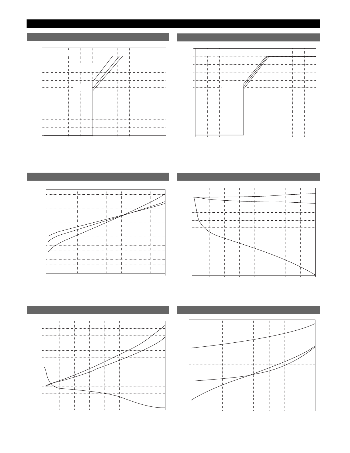
Typical Performance Characteristics
CS8140/1
5.5
V
OUT
vs. VINover R
LOAD
; T = 25ûC
V
OUT
vs. VINover Temperature; R
LOAD
= 25½
Dropout Voltage vs. Output Current over Temperature
Load Regulation vs. Output Current over Temperature
Line Regulation vs. Output Current over Temperature
Quiescent Current vs. Output Current over Temperature
(V)
OUT
V
5.0
4.5
4.0
3.5
3.0
2.5
2.0
1.5
1.0
0.5
0.0
V
ENABLE
01 23456 78910
= V
IN
R
load
R
load
= NO LOAD
= 10W
VIN (V)
R
= 6.67W
load
5.5
V
= V
ENABLE
5.0
4.5
4.0
3.5
(V)
3.0
OUT
2.5
V
2.0
1.5
1.0
0.5
0.0
01 23456 78910
IN
TEMP = 125°C
TEMP = -40 °C
TEMP = 25°C
VIN (V)
1800
1600
1400
1200
V
IN
-40°C
25°C
= 14V
125°C
I
25°C
I
OUT
OUT
(mA)
-40°C
125°C
(mA)
1000
800
600
Dropout Voltage (mV)
400
200
0
0 100 200 300 400 500 600 700 800
18
16
14
12
10
8
6
4
2
0
LINE REGULATION (mV)
-2
-4
-6
0 100 200 300 400 500 600 700 800
3.5
0
-3.5
-7.0
-10.5
-14.0
-17.5
-21.0
-24.5
LOAD REGULATION (mV)
-28.0
-31.5
-35.0
10
9
8
7
(mA)
Q
I
6
5
4
0 100 200 300 400 500 600 700 800
25°C
125°C
0 100 200 300 400 500 600 700 800
I
(mA)
OUT
VIN = 14V
-40°C
125°C
25°C
I
(mA)
OUT
V
IN
-40°C
= 14V
 Loading...