

CHERRY Semiconductor CS8135 Service Manual
1
Features
■ Two Regulated Outputs
Primary Output 5V
± 5%; 500mA
Secondary Standby 5V
±5%; 10mA
■ Low Dropout Voltage
(0.6V at 0.5A)
■ ON/OFF Control
Option
■ Low Quiescent Drain
(<3mA)
■ RESET Option
■ Protection Features
Reverse Battery
60V Load Dump
-50V Reverse Transient
Short Circuit
Thermal Shutdown
Overvoltage Shutdown
Package Option
5 Lead TO-220
Tab (Gnd)
1
CS8135
5V, 5V Low Dropout Dual Regulator
with /ENABLE
RESET
CS8135
Description
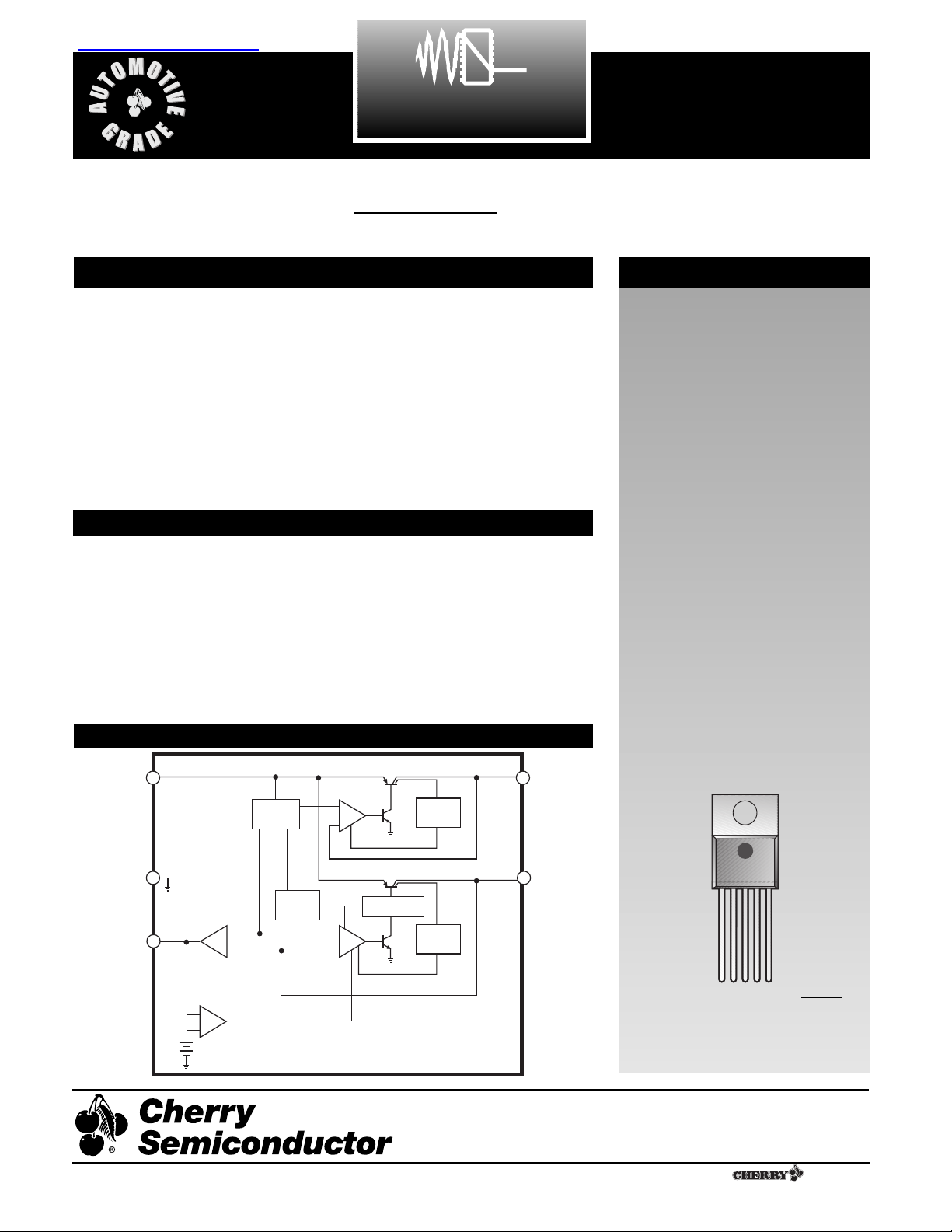
Block Diagram
Absolute Maximum Ratings
Input Voltage
Operating Range.....................................................................-0.5V to 26V
Load Dump ............................................................................................60V
Internal Power Dissipation..................................................Internally Limited
Junction Temperature Range (T
J
)............................................-40¡C to +150¡C
Storage Temperature Range ....................................................-65¡C to +150¡C
Lead Temperature Soldering
Wave Solder (through hole styles only)..........10 sec. max, 260¡C peak
Electrostatic Discharge (Human Body Model) ..........................................2kV
The CS8135 is a low dropout, high current, dual 5V linear regulator. The secondary 5V/10mA output is often used
for powering systems with standby
memory. Quiescent current drain is
less than 3mA when supplying 10mA
loads from the standby regulator.
In automotive applications, the CS8135
and all regulated circuits are protected
from reverse battery installations, as
well as two-battery jumps. During line
transients, such as a 60V load dump,
the 500mA output will automatically
shut down the primary output to protect both internal circuits and the load.
The standby regulator will continue to
power any standby load.
The CS8135 is packaged in a 5 lead
TO-220.
NOTE: The CS8135 is compatible with
the LM2935.
1V
IN
2V
OUT1
3 Gnd
4/
ENABLE
5V
OUT2
RESET
A Company
¨
Rev. 10/21/97
Cherry Semiconductor Corporation
2000 South County Trail, East Greenwich, RI 02818
Tel: (401)885-3600 Fax: (401)885-5786
Email: info@cherry-semi.com
Web Site: www.cherry-semi.com
查询CS8135YT5供应商
V
IN
Bandgap
Reference
Standby Output
+
-
Output
Current
Limit
V
OUT2
RESET/
ENABLE
Gnd
Primary Output
Thermal
Shutdown
+
-
+
-
+
-
Over Voltage
Shutdown
Output
Current
Limit
V
OUT1

2
CS8135
PARAMETER TEST CONDITIONS MIN TYP MAX UNIT
Electrical Characteristics : V
IN
= 14V, I
OUT1
= 5mA, I
OUT2
= 1mA, -40¡C ² TA² 125¡C, -40¡C ² TJ² 150¡C unless otherwise specified
■ Output Stage (V
OUT1
)
Output Voltage, V
OUT1
6V ² VIN² 26V, 5mA ² I
OUT1
² 500mA 4.75 5.00 5.25 V
Dropout Voltage I
OUT
= 500mA 0.35 0.60 V
I
OUT
= 750mA 0.50 V
Line Regulation 6V ² VIN² 26V, I
OUT1
= 5mA 10 50 mV
Load Regulation 5mA ² I
OUT
² 500mA 10 50 mV
Quiescent Current I
OUT1
² 10mA, No Load on Standby 3 7 mA
I
OUT1
= 500mA, No Load on Standby 30 100 mA
I
OUT1
= 750mA, No Load on Standby 60 150 mA
Ripple Rejection f = 120Hz 66 dB
Current Limit 0.75 1.40 A
Maximum Line Transient V
OUT1
² 5.5V 90 V
Reverse Polarity V
OUT1
³ -0.6V, 10½ Load -50 V
Input Voltage, DC
Reverse Polarity Input 1% Duty Cycle, t = 100ms, V
OUT1
³ -6V, -80 V
Voltage, Transient 10½ Load
Output Noise Voltage 10Hz-100kHz 100 µVrms
Long Term Stability 20 mV/khr
Output Impedance 500mA DC and 10mA rms, 200 m½
100Hz-10kHz
Overvoltage Shutdown 30 V
■ Standby Output (V
OUT2
)
Output Voltage (V
OUT2
) 6V ² VIN² 26V, 1mA ² I
OUT1
² 10mA 4.75 5.00 5.25 V
Dropout Voltage I
OUT2
= 10mA 0.3 0.7 V
Tracking V
OUT1-VOUT2
50 200 mV
Line Regulation 6V ² VIN² 26V 4 50 mV
Load Regulation 1mA ² I
OUT1
² 10mA 10 50 mV
Quiescent Current I
OUT
² 10mA, V
OUT
OFF 2 3 mA
Ripple Rejection f = 120Hz 66 dB
Current Limit 25 70 mA
Output Noise Voltage 10Hz-100kHz 300 µV
Long Term Stability 20 mV/khr
Output Impedance 10mA DC and 1mA rms, 100Hz-10kHz 1 ½
■ Function
Output Voltage
Low R1= 20k½, VIN= 4.5V See Test & Application Circuit 0.8 1.1 V
High R1= 20k½, VIN= 14V (page 6) 4.5 5.0 6.0 V
Output Current VIN= 4.5V, in Low State 5 mA
ON/OFF Resistor R1 (±10% Tolerance) 20 30 k½
RESET
RESET
RESET
RESET
3
CS8135
Package Lead Description
PACKAGE LEAD # LEAD SYMBOL FUNCTION
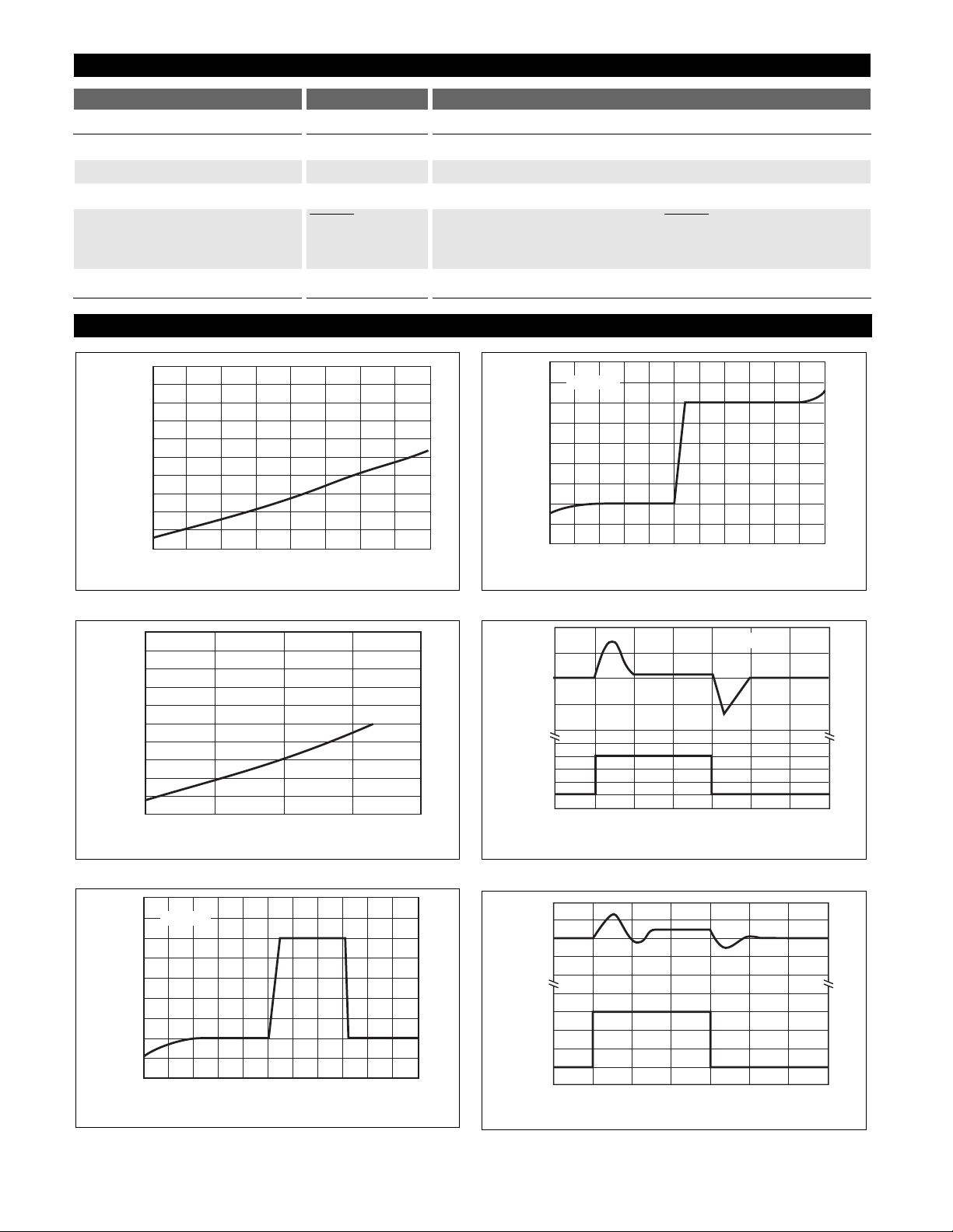
Typical Performance Characteristics
TO-220
1V
IN
Supply voltage to IC, usually direct from battery.
2V
OUT1
Regulated output voltage 5V, 500mA (typ) switched.
3 Gnd Ground connection.
4 /ENABLE CMOS compatible output lead, goes low whenever
V
OUT1
becomes unregulated. To use the ENABLE option, con-
nect the lead via a resistor to VIN(see app. notes).
5V
OUT2
STANDBY output 5V, 10mA typ, always on.
RESET
RESET
Dropout Voltage vs. Output Current
Standby Dropout Voltage vs. Output Current
Output Voltage vs. Input Voltage
Standby Output Voltage vs. Input Voltage
Line Transient Response (V
OUT1
)
Line Transient Response (V
OUT2
)
10
TIME (ms)
INPUT VOLTAGE
CHANGE (V)
OUTPUT VOLTAGE
DEVIATION (mV)
5
0
-5
-10
3
2
1
0
0102030405060
20
10
0
-10
-20
3
2
1
0
0 1020 304050 60
TIME (ms)
INPUT VOLTAGE
CHANGE (V)
OUTPUT VOLTAGE
DEVIATION (mV)
I
OUT
1
=500mA
7
6
5
4
3
2
1
0
-1
-2
-40 -20 0 20 40 60
INPUT VOLTAGE (V)
OUTPUT VOLTAGE (V)
RL=500W
7
6
5
4
3
2
1
0
-1
-2
-40 -20 0 20 40 60
INPUT VOLTAGE (V)
OUTPUT VOLTAGE (V)
RL=10W
1.0
0.9
0.8
0.7
0.6
0.5
0.4
0.3
0.2
0.1
0.0
INPUT-OUTPUT DIFFERENTIAL VOLTAGE (V)
OUTPUT CURRENT (mA)
0 5 10 15 20
1.0
0.9
0.8
0.7
0.6
0.5
0.4
0.3
0.2
0.1
0.0
INPUT-OUTPUT DIFFERENTIAL VOLTAGE (V)
OUTPUT CURRENT (mA)
0 200 400 600 800
 Loading...