

Cherry Semiconductor CS8127YN8, CS8127YD8, CS8127YDR8 Datasheet
1
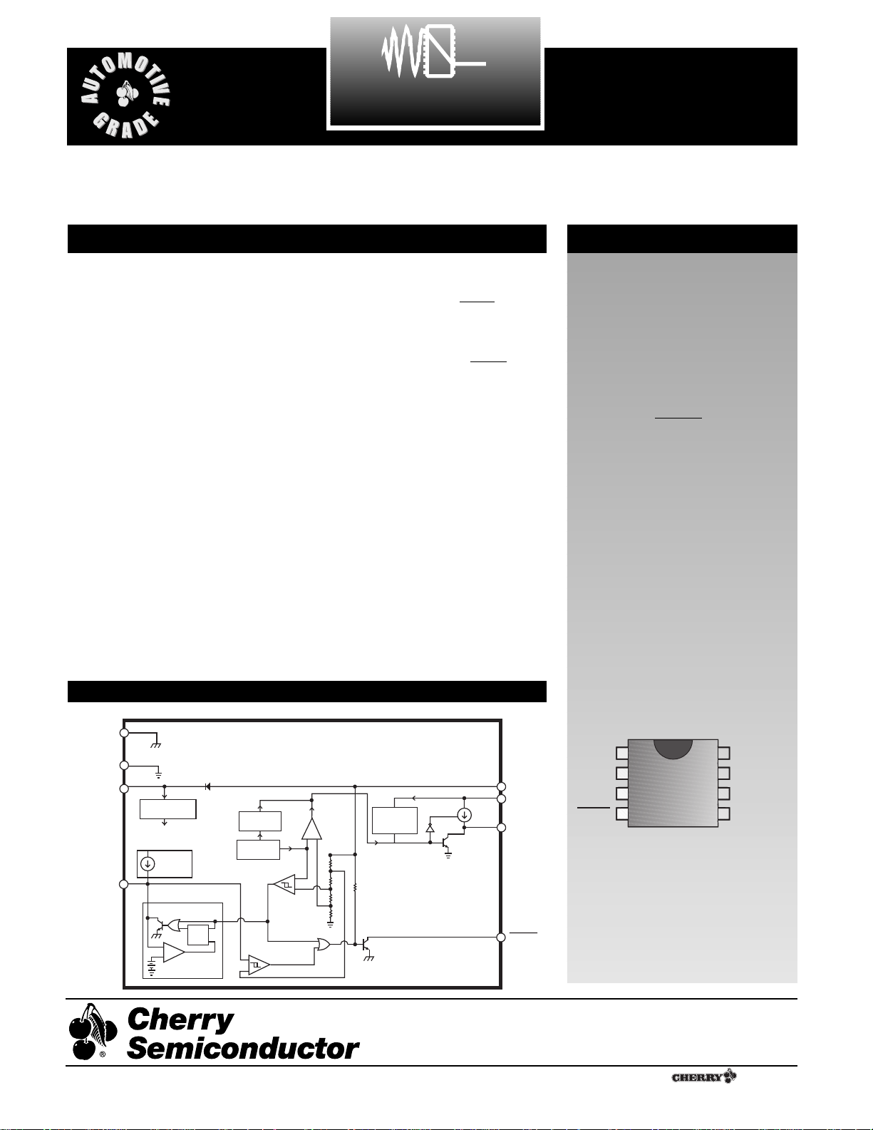
The CS8127 contains all the necessary
control circuitry to implement a 5V linear regulator. An external pass device is
used to produce superior performance
compared to conventional monolithic
regulators. The CS8127 with a TIP42
PNP transistor typically provides a
100mV dropout voltage at 500mA,
increasing to 350mV at 3A. Quiescent
current at 500mA is only 5mA.
Monolithic regulators cannot approach
these figures because their power transistors do not provide the high beta and
excellent saturation characteristics at
high currents. The CS8127 is compatible
with a wide variety of external transistors, allowing flexibility for thermal,
space, and cost management.
The CS8127 includes thermal shutdown,
externally programmable current limit,
and over-voltage shutdown, making it
suitable for use in automotive and
switching regulator post regulator applications. An optional external RC filter
added to the CS8127 supply lead provides EMC hardening in addition to the
on-chip EMC hardening. The SENSE
lead allows remote sensing of the output
voltage for improved regulation.
An active microprocessor RESET function is included on-chip with externally
programmable delay time. During
power-up, or after detection of any error
in the regulated output, the RESET lead
will remain in the low state for the duration of the delay. Types of errors include
short circuit, low input voltage, overvoltage shutdown, thermal shutdown,
or others that cause the output to
become unregulated. This function is
independent of the input voltage and
will function correctly with an output
voltage as low as 1V. Hysteresis is
included in both the reset and delay
comparators for noise immunity and to
prevent oscillations. A latching discharge circuit is used to discharge the
delay capacitor, even when triggered by
a relatively short fault condition. This
circuit improves upon the commonly
used SCR structure by providing
improved noise immunity and full
capacitor discharge (0.2V typ).
Features
■ Externally Set Delay for
Reset
■ 60V Peak Transient
Capability
■ Internal Thermal
Overload Protection
■ 3% Output Accuracy
■ Active RESET
■ Noise Immunity
■ On Chip EMC Hardening
Protection Incorporated
■ Externally Set Current
Limit
Package Options
8L SO & 8L PDIP
CS8127
5V Linear Controller/Driver
1
V
IN
2
3
4
Sense
Delay
V
OUT
Pwr Gnd
Pullup
Ref Gnd
8
7
6
5
RESET
CS8127
Description
Block Diagram
A Company
¨
Rev. 2/12/99
Cherry Semiconductor Corporation
2000 South County Trail, East Greenwich, RI 02818
Tel: (401)885-3600 Fax: (401)885-5786
Email: info@cherry-semi.com
Web Site: www.cherry-semi.com
Pwr Gnd
Ref Gnd
V
IN
Delay
IC
Power
Gnd
IC
Reference
Gnd
PRE-
REGULATOR
Regulated Supply
for Circuit Bias
10mA
Delay
Current
Latching
Discharge
-
+
V
dis
Q
S
R
Thermal
Shutdown
Bandgap
Reference
Delay
Comparator
-
+
Reset
Comparator
1.25V
Error
Amp
+
-
+
-
Over
Voltage
Shutdown
50mA
Sense
PULLUP
V
OUT
RESET
2
Note 1: Dependent on characteristics of external transistor.
Electrical Characteristics: T
A
=-40ûC to +125ûC, TJ=-40ûC to +150ûC, VIN=6 to 26V, I
OUT
=5 to 500mA, Per Test Circuit
(unless otherwise noted)
PARAMETER TEST CONDITIONS MIN TYP MAX UNIT
Absolute Maximum Ratings
Power Dissipation.............................................................................................................................................Internally Limited
Input Voltage ..................................................................................................................................................................Ð0.3V, 26V
Transient Input Voltage ............................................................................................................................................................60V
Output Current ...............................................................................................................................................Externally Limited
ESD Susceptibility (Human Body Model)..............................................................................................................................2kV
Junction Temperature ............................................................................................................................................Ð45¡C to 150¡C
Storage Temperature..............................................................................................................................................Ð55¡C to 150¡C
Lead Temperature Soldering
Wave Solder (through hole styles only) .....................................................................................10 sec. max, 260¡C peak
Reflow (SMD styles only) ......................................................................................60 sec. max above 183¡C, 230¡C peak
CS8127
C
Delay
x V
DTC
I
Charge
Note 2: Delay Time =
= C
Delay
x 3.5 x 10⁵(Typical)
■ Output Stage (V
OUT
)
Output Voltage 4.85 5.00 5.15 V
Dropout Voltage I
OUT
= 500mA, note 1 0.1 0.6 V
Supply Current I
Q
I
OUT
² 10mA 4 8 mA
I
OUT
² 500mA 5 15
I
OUT
² 3A, note 1 30
Line Regulation 6V ² V
IN
² 26V, I
OUT
= 5mA 12 50 mV
Load Regulation 5V ² I
OUT
² 500mA, VIN= 14V 2 50 mV
Ripple Rejection f = 120Hz, 7V ² V
IN
² 17V, 60 70 dB
I
OUT
= 350mA
VINOvervoltage Shutdown 32 40 V
Drive Current V
SENSE
= 6V 50 µA
V
SENSE
= 0V 25 250 mA
■ and Delay Functions
Delay Charge Current, I
Charge
V
Delay
= 2V 5 10 15 µA
Threshold V
RTH
V
OUT
Increasing 4.65 4.90 V
OUT
-0.10 V
V
RTL
V
OUT
Decreasing 4.50 4.70 V
OUT
-0.15 V
Hysteresis V
RH
150 200 250 mV
Delay Threshold V
DTC
Charge 3.25 3.50 3.75 V
V
DTD
Discharge 2.80 3.00 3.40 V
Delay Hysteresis, V
DH
V
DTC
- V
DTD
200 400 800 mV
Output Voltage Low 1V < V
OUT
< V
RTL
, 3k½ to V
OUT
0.4 V
Output VD> V
DTC
, V
OUT>VRTH
10 µA
Leakage Current
Delay Capacitor (V
dis
) Discharge Latched "ON", 0.2 0.5 V
Discharge Voltage V
OUT
> V
RTH
Delay Time C
Delay
= 0.1µF, note 2 16 32 48 ms
RESET
RESET
RESET
RESET
RESET
 Loading...