

Cherry Semiconductor CS8121YTVA5, CS8121YTHA5, CS8121YT5, CS8121YDPSR7, CS8121YDPS7 Datasheet
...
The CS8121 is a 5V, 1A precision linear
regulator with two microprocessor
compatible control functions and protection circuitry included on chip. The
composite NPN-PNP output pass transistor assures a lower dropout voltage
(1.2V @ 1A) without requiring excessive supply current (4mA).
The CS8121Õs two logic control functions make this regulator well suited to
applications requiring microprocessorbased control at the board or module
level. controls the output
stage. A high voltage (>2.9V) on
the lead turns off the regulatorÕs pass transistor and sends the IC
into Sleep mode where it draws only
250µA. sends a signal
when the IC is powering up or whenever the output voltage falls out of regulation. The signal is valid
down to V
OUT
= 1V.
The CS8121 design optimizes supply
rejection by switching the internal
bandgap reference from the supply
input to the regulator output as soon as
the nominal output voltage is achieved.
Additional on chip filtering enhances
rejection of high frequency transients
on all external leads.
The CS8121 is fault protected against
short circuit, over voltage and thermal
runaway conditions.
RESET
RESETRESET
ENABLE
ENABLE
1
Features
■
5V ± 4% Output Voltage
■ Low Dropout Voltage
(1.2V @ 1A)
■ Low Quiescent Current
(4mA @ I
OUT
= 1A)
■ µP Compatible Control
Functions
■ Low Current Sleep Mode
I
Q
= 250µA
■ Fault Protection
Thermal Shutdown
Short Circuit
60V Peak Transient
Voltage
ENABLE
RESET
Package Options
5 Lead TO-220
5 Lead TO-220
Overmolded
1
CS8121
5V, 1A Linear Regulator
with and
ENABLE
RESET
CS8121
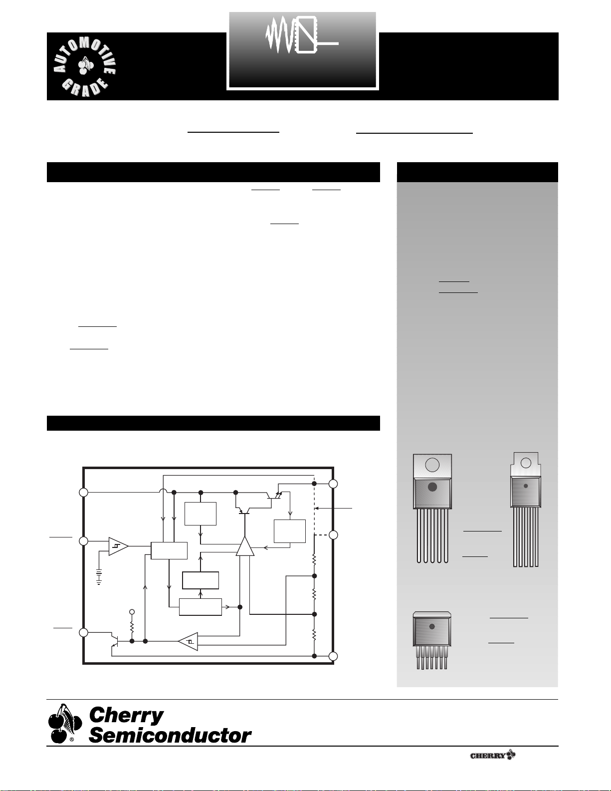
Description
Block Diagram
1
1V
IN
2
3 Gnd
4
5V
OUT
RESET
ENABLE
7 Lead D
2
PAK
1
1NC
2V
IN
3
4 Gnd
5
6V
OUT
7V
OUT(SENSE)
RESET
ENABLE
Cherry Semiconductor Corporation
2000 South County Trail, East Greenwich, RI 02818
Tel: (401)885-3600 Fax: (401)885-5786
Email: info@cherry-semi.com
Web Site: www.cherry-semi.com
A Company
¨
Rev. 5/4/99
V
IN
ENABLE
-
ENABLE
RESET
Comparator
+
V
REF
TO V
OUT
Bandgap
Supply
RESET
Comparator
Output
Current
Limit
-
+
Amplifier
Error
Over
Voltage
Shutdown
Thermal
Shutdown
Bandgap
Reference
+
-
V
OUT
5 Lead
TO-220
V
OUT(SENSE)
Gnd
2
Electrical Characteristics: I
OUT
= 5mA, -40ûC ² TJ ²150ûC , 7V ² V
IN
² 26V, -40¡C ² TA ² 125¡C unless otherwise specified
PARAMETER TEST CONDITIONS MIN TYP MAX UNIT
CS8121
Absolute Maximum Ratings
DC Input Voltage ...........................................................................................................................................................-0.7 to 26V
Peak Transient Voltage (46V Load Dump).............................................................................................................................60V
Output Current .................................................................................................................................................Internally Limited
Electrostatic Discharge (Human Body Model)......................................................................................................................2kV
Operating, Temperature ..........................................................................................................................................-40C to 125¡C
Junction Temperature...............................................................................................................................................-40C to 150¡C
Storage Temperatures.............................................................................................................................................-55¡C to 150¡C
Lead Temperature Soldering
Wave Solder (through hole styles only) .....................................................................................10 sec. max, 260¡C peak
Reflow (SMD styles only) ......................................................................................60 sec. max above 183¡C, 230¡C peak
■ Output Stage
Output Voltage, V
OUT
7V ² V
IN
² 26V, 1mA ² I
OUT
² 1A 4.8 5.0 5.2 V
Line Regulation 7V ² V
IN
² 26V, I
OUT
= 5mA 0 50 mV
Load Regulation 5mA ² I
OUT
²1A 10 70 mV
Supply Voltage Rejection VIN= 14VDC+ 1V
RMS
54 70 dB
@120Hz, I
LOAD
= 50½
Dropout Voltage I
OUT
= 1A 1.2 1.8 V
Quiescent Current = High, V
IN
= 12V 0.25 0.65 mA
= Low, I
OUT
= 1A 4 20 mA
■ Protection Circuits
Short Circuit Current 1.5 A
Thermal Shutdown 150 190 ûC
Overvoltage Shutdown 26 40 V
■
Saturation Voltage 1V < V
OUT
< V
RT(OFF),
3.1k½ pull-up 0.1 0.4 V
to V
OUT
Output Leakage = Low 0 25 µA
Current V
OUT
> V
RT(ON)
, V = V
OUT
Power ON/OFF 3.1k½ pull-up to V
OUT
0.7 1.0 V
Peak Output Voltage
Threshold ON V
OUT
- 0.10 V
OUT
- 0.04 V
(V
OUT
Increasing)
Threshold OFF 4.75 V
OUT
- 0.14 V
(V
OUT
Decreasing)
Threshold Hysteresis 10 40 mV
■
Input High Voltage 7V < V
IN
< 26V 2.9 3.9 V
Input Low Voltage 7V < V
IN
< 26V 1.1 2.1 V
Input Hysteresis 7V < V
IN
< 26V 0.4 0.8 2.8 V
Input Current Gnd < V
IN(HI)
< V
OUT
0 ±10 µA
ENABLE
RESET
RESET
RESET
RESET
RESET
ENABLERESET
RESET
RESET
ENABLE
ENABLE
3
CS8121
Package Lead Description
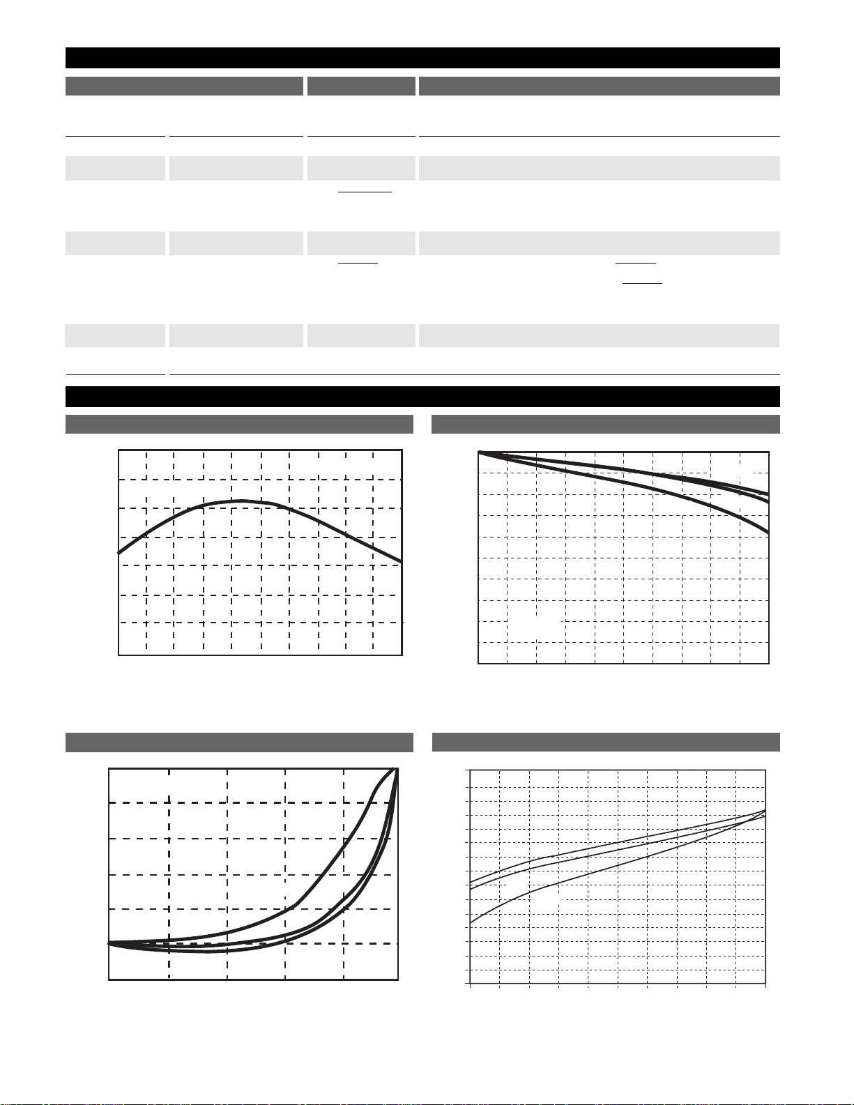
Typical Performance Characteristics
PACKAGE LEAD # LEAD SYMBOL FUNCTION
Junction Temperature (ûC)
-40
-20 0 20 40 60 80 100 120 140 150
5.02
5.01
5
4.99
4.98
4.97
4.96
4.95
I
OUT = 100mA
V
OUT
(V)
5.00V @ 25ûC
Output Voltage vs. Temperature
Load Regulation vs. Output Current Over Temperature
Line Reg. (mV)
VIN = 7 to 26V
-40ûC
125ûC
25ûC
50
40
30
20
10
0
-10
I
OUT
(A)
0
0.2
0.4
0.6
0.8
1A
Line Regulation vs. Output Current Over Temperature
1.5
1.4
1.3
1.2
1.1
1.0
0.9
0.8
0.7
0.6
0.5
0.4
0.3
0.2
0.1
0.0
0 0.2 0.6 0.9 1.0
0.1 0.3 0.50.4 0.7 0.8
I
OUT
(A)
Dropout Voltage (V)
-40°C
25°C
125°C
Dropout Voltage vs. Output Current Over Temperature
7 Lead 5 Lead TO-220 &
D2PAK Overmolded TO-220
1 NC No Connection.
21V
IN
Supply voltage to IC, usually direct from the battery.
3 2 CMOS compatible logical. V
OUT
is disabled i.e. placed in a
high impedance state when ENABLE is high.
4 3 Gnd Ground connection.
5 4 CMOS compatible output lead. goes low whenever
V
OUT
falls out of regulation. The delay is externally
programmed.
65V
OUT
Regulated output voltage, 5V (typ).
7V
OUT(SENSE)
Remote sensing of output voltage.
RESET
RESETRESET
ENABLE
0
-5
-10
-15
-20
-25
-30
Load Reg. (mV)
-35
-40
-45
-50
0 200 400 600 800 1A
VIN =14V
I
OUT
125° C
(A)
Ð40° C
25° C
 Loading...