

Cherry Semiconductor CS8101YTVA5, CS8101YTHA5, CS8101YT5, CS8101YDWFR20, CS8101YDWF20 Datasheet
...
The CS8101 is a precision 5V
micropower voltage regulator with
very low quiescent current (70µA
typ at 100µA load). The 5V output is
accurate within ±2% and supplies
100mA of load current with a typical dropout voltage of only 400mV.
Microprocessor control logic
includes an input and an
active . This combination of
low quiescent current, outstanding
regulator performance and control
logic makes the CS8101 ideal for
any battery operated, microprocessor controlled equipment.
The active circuit includes
hysteresis, and operates correctly at
an output voltage as low as 1V. The
function is activated during
the power up sequence or during
normal operation if the output
voltage drops outside the regulation
limits by more than 200mV typ. The
logic level compatible
input allows the user to put the regulator into a shutdown mode where
it draws only 20µA typical of quiescent current.
The regulator is protected against
reverse battery, short circuit, over
voltage, and thermal overload conditions. The device can withstand
load dump transients making it
suitable for use in automotive environments.
The CS8101 is functionally equivalent to the National Semiconductor
LP2951 series low current regulators.
ENABLE
RESET
RESET
RESET
ENABLE
1
Features
■ 5V ±2% Output
■ Low 70µA Quiescent
Current
■ Active
■ Input for
ON/OFF and Active/Sleep
Mode Control
■ 100mA Output Current
Capability
■ Fault Protection
+60V Peak Transient
Voltage
-15V Reverse Voltage
Short Circuit
Thermal Overload
■ Low Reverse Current
(Output to Input)
ENABLE
RESET
Package Options
CS8101
Micropower 5V, 100mA Low Dropout
Linear Regulator with RESET and ENABLE
CS8101
Description
Block Diagram
1
V
OUT
V
OUT
Sense
ENABLE
Gnd
V
IN
NC
NC
RESET
5L TO-220
Tab (Gnd)
1. V
OUT
2.
3. Gnd
4.
5. V
IN
RESET
ENABLE
Other Packages: D2PAK (consult factory)
8L SOIC
V
OUT
V
IN
NC
NC
RESET
Gnd
Gnd
Gnd
Gnd
Gnd
Gnd
Gnd
Gnd
ENABLE
NC
NC
NC
NC
NC
NC
NC
20L SOIC Wide
(Internally Fused Leads)
Rev. 4/9/99
Cherry Semiconductor Corporation
2000 South County Trail, East Greenwich, RI 02818
Tel: (401)885-3600 Fax: (401)885-5786
Email: info@cherry-semi.com
Web Site: www.cherry-semi.com
A Company
¨
V
ENABLE
IN
Current Source
(Circuit Bias)
Shutdown
Over
Voltage
Current Limit
Sense
V
OUT
Internally connected
on 5 lead TO-220
V
Sense
OUT
1
RESET
+ -
Error
Thermal
Protection
Amplifier
Bandgap
Reference
+
-
Reset
Comparator
Gnd
2
Power Dissipation.............................................................................................................................................Internally Limited
Transient Peak Voltage (46V Load Dump) ..................................................................................................................-15V, 60V
Output Current .................................................................................................................................................Internally Limited
ESD Susceptibility (Human Body Model) ..............................................................................................................................2kV
Operating Temperature..........................................................................................................................................-40¡C to 125¡C
Junction Temperature .............................................................................................................................................-40¡C to 150¡C
Storage Temperature ................................................................................................................................................-55C to 150¡C
Lead Temperature Soldering Wave Solder (through hole styles only) ..........................................10 sec. max, 260¡C peak
Reflow (SMD styles only) ..........................................60 sec. max above 183¡C, 230¡C peak
Electrical Characteristics: 6V ² V
IN
² 26V, I
OUT
= 1mA, -40 ² TA² 125, -40 ² TJ² 150¡C unless otherwise specified.
PARAMETER TEST CONDITIONS MIN TYP MAX UNIT
CS8101
Absolute Maximum Ratings
■ Output Stage
Output Voltage, V
OUT
9V < VIN< 16V, 100µA ² I
OUT
² 100mA 4.90 5.00 5.10 V
6V ² VIN² 26V, 100µA ² I
OUT
² 100mA 4.85 5.00 5.15 V
Dropout Voltage (VIN-V
OUT
)I
OUT
= 100mA 400 600 mV
I
OUT
= 100µA 100 150 mV
Load Regulation VIN= 14V, 100µA ² I
OUT
² 100mA 5 50 mV
Line Regulation 6V < V < 26V, I
OUT
= 1mA 5 50 mV
Quiescent Current, (IQ)
Active Mode I
OUT
= 100µA, VIN= 6V 70 140 µA
I
OUT
= 50mA 4 6 mA
I
OUT
² 100mA 12 20 mA
Sleep Mode V
OUT
= OFF, VIN= 6V, V = 2V 20 50 µA
Ripple Rejection 7 ² VIN² 17V, I
OUT
= 100mA, f = 120Hz 60 75 dB
Current Limit 105 200 mA
Short Circuit Output Current V
OUT
= 0V 25 125 mA
Thermal Shutdown 150 180 ¡C
Overvoltage Shutdown V
OUT
²1V 303438V
Reverse Current V
OUT
= 5V, VIN= 0V 100 200 µA
■ Enable Input ( )
Threshold
HIGH (V
OUT
OFF) 1.4 2.0 V
LOW (V
OUT
ON) 0.6 1.4 V
Input Current V = 2.4V 30 100 µA
■ Reset Function ( )
Threshold
HIGH (VRH)V
OUT
Increasing 4.525 4.75 V
OUT
- 0.05 V
LOW (VRL)V
OUT
Decreasing 4.500 4.700 V
OUT
- 0.075 V
Hysteresis (HIGH - LOW) 25 50 100 mV
Reset Output Leakage V
OUT³VRH
25 µA
= HIGH
Output Voltage
Low (V
RLO
) 1V ² V
OUT²VRL
0.1 0.4 V
R = 10K
Low (VRpeak) V
OUT
, Power up, Power down 0.6 1.0 V
RESET
RESET
RESET
RESET
RESET
ENABLE
ENABLE
ENABLE
Output Stage Protection
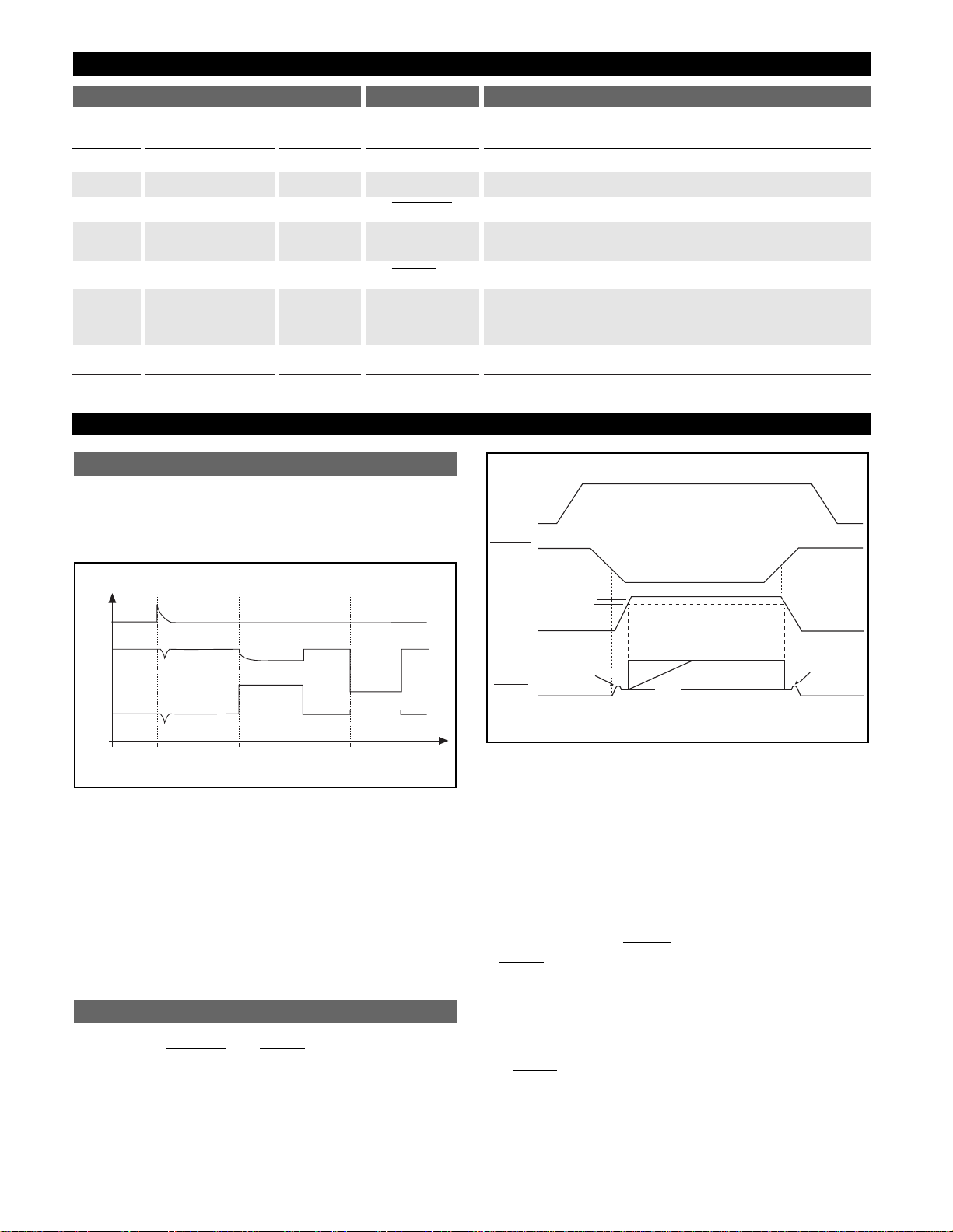
The output stage is protected against overvoltage, short
circuit and thermal runaway conditions (Figure 1).
Figure 1. Typical Circuit Waveforms for Output Stage Protection.
If the input voltage rises above 30V (e.g. load dump), the output shuts down. This response protects the internal circuitry
and enables the IC to survive unexpected voltage transients.
Should the junction temperature of the power device exceed
180ûC (typ) the load current capability is reduced thereby
preventing thermal overload. This thermal management
function is an effective means to prevent die overheating
since the load current is the principle heat source in the IC.
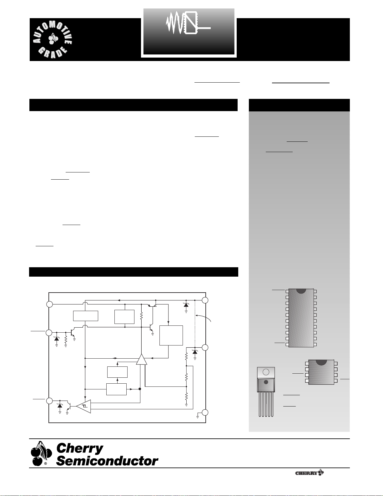
The CS8101 contains two microprocessor compatible control functions: and (Figure 2).
Figure 2. Circuit Waveform
Function
The function switches the output transistor ON
and OFF. When the voltage on the lead exceeds
1.4V typ, the output pass transistor turns off, leaving a
high impedance facing the load. The IC will remain in
Sleep mode, drawing only 50µA, until the voltage on this
input drops below the threshold.
Function
A signal (low voltage) is generated as the IC powers up until V
OUT
is within 250mV of the regulated output
voltage, or when V
OUT
drops out of regulation,and is
lower than 300mV below the regulated output voltage. A
hysteresis of 50mV is included in the function to minimize
oscillations.
The output is an open collector NPN transistor,
controlled by a low voltage detection circuit. The circuit is
functionally independent of the rest of the IC thereby
guaranteeing that the signal is valid for V
OUT
as low
as 1V.
RESET
RESET
RESET
RESET
ENABLE
ENABLE
ENABLE
ENABLE
RESETENABLE
Regulator Control Functions
Voltage Reference and Output Circuitry
3
CS8101
Package Lead Description
PACKAGE LEAD # LEAD SYMBOL FUNCTION
Circuit Description
8 Lead 20 Lead SOIC 5 Lead
SOIC (Internally Fused Leads) TO-220
819 5VINInput voltage.
120 1V
OUT
5V, ±2%, 100mA output.
3 1 2 Logic level switches output off when toggled HIGH.
4 4,5,6,7 3 Gnd Ground. All Gnd leads must be connected to Ground.
14,15,16,17
5 10 4 Active reset (accurate to V
OUT
³ 1V).
2V
OUT
Sense Kelvin connection which allows remote sensing of out-
put voltage for improved regulation. If remote sensing
is not required, connect to V
OUT
.
6,7 2,3,8,9,11,12,13,18 NC No Connection.
RESET
ENABLE
> 30V
V
IN
V
OUT
I
OUT
Load
Dump
Current
Limit
Short
Circuit
FOR 7V < V
V
IN
ENABLE
V
IN
H
V
RH
V
V
OUT
RESET
RL
VR
(1)
PEAK
VR
LO
(1) = NO RESET DELAY CAPACITOR
(2) = WITH RESET DELAY CAPACITOR
IN
(2)
< 26V
VR
PEAK
 Loading...