

Cherry Semiconductor CS5661EDWR16, CS5661EDW16 Datasheet
1
Features
■ Oscillator has Precise
Duty Cycle
Limit and Frequency
Control
■ 500kHz Current Mode
Operation
■ Automatic Feed Forward
Compensation
■ Separate Latching PWMs
for Cycle-By-Cycle
Current Limiting
■ Internally Trimmed
Reference with
Undervoltage Lockout
■ Switchable Second
Output
■ Two High Current Totem
Pole Outputs
■ Input Undervoltage
Lockout with Hysteresis
■ 8.4V Start Up Voltage
Threshold
Package Options
16 Lead SO Wide
CS5661
High Performance Dual Channel
Current Mode Controller with ENABLE
1
SYNC
2
3
4
5
6
7
8
C
T
R
T
V
FB
1
COMP
1
SENSE
1
V
OUT
1
Gnd
16
15
14
13
12
11
10
9
V
CC
V
REF
ENABLE
2
V
FB
2
COMP2
SENSE
2
V
OUT
2
Pwr Gnd
CS5661
Description
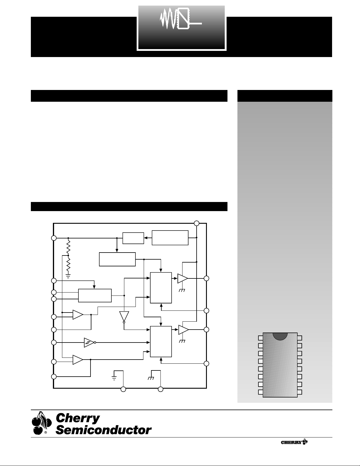
The CS5661 is a high performance,
fixed frequency, dual current mode
controller specifically designed for
Off-Line and DC to DC converter
applications. It offers the designer a
cost effective solution with minimal
external components. This integrated circuit features a unique oscillator for precise duty cycle limit and
frequency control, a temperature
compensated reference, two high
gain error amplifiers, two current
sensing comparators, and two high
current totem pole outputs ideally
suited for driving power MOSFETs.
V
OUT
2
output is switchable via the
ENABLE2pin.
Also included are protective features consisting of input and reference undervoltage lockouts, each
with hysteresis, cycle-by-cycle current limiting, and a latch for single
pulse metering of each output.
The CS5661 is pin compatible with
the MC34065L.
Block Diagram
Rev. 2/2/99
Cherry Semiconductor Corporation
2000 South County Trail, East Greenwich, RI 02818
Tel: (401)885-3600 Fax: (401)885-5786
Email: info@cherry-semi.com
Web Site: www.cherry-semi.com
A Company
®
V
REF
Undervoltage
SYNC
C
T
R
T
Oscillator
V
Undervoltage
Lockout
Latching
PWM 1
CC
V
REF
Lockout
5.0V Ref
V
CC
V
OUT
1
COMP
ENABLE
COMP
Sense
1
V
OUT
2
Sense
2
+
-
Error
Amp 1
+
-
Amp 2
Error
Latching
PWM 2
Gnd
Pwr Gnd
V
FB
1
1
2
V
FB
2
2
2
Electrical Characteristics: (V
CC
= 15V, RT= 8.2kΩ, CT= 3.3nF, for typical values TA= 25˚C, for min/max values -40˚C < TA < 85˚C,
unless otherwise stated.
PARAMETER TEST CONDITIONS MIN TYP MAX UNIT
Absolute Maximum Ratings
Output Current, Source or Sink (Note 1)......................................................................................................................400mA
Output Energy (capacitive load per cycle) .......................................................................................................................5.0µJ
Current Sense, Enable and Voltage......................................................................................................................-0.3 to +5.5V
Feedback Inputs
Sync Input – High State (Voltage) ......................................................................................................................................5.5V
– Low State (Reverse Current) ...................................................................................................................-5.0mA
Error Amp Output Sink Current......................................................................................................................................10mA
Storage Temperature Range ................................................................................................................................-65 to +150°C
Operating Junction Temperature...................................................................................................................................+150°C
Lead Temperature Soldering
Reflow (SMD styles only) ......................................................................................60 sec. max above 183°C, 230°C peak
ESD Capability (Human Body Model) ...................................................................................................................................2kV
CS5661
■ Reference Section
Reference Output Voltage, I
OUT
= 1.0mA, TJ= 25°C 4.9 5.0 5.1 V
V
REF
Line Regulation 11V ≤ VCC≤ 15V 2.0 20.0 mV
Load Regulation 1.0mA ≤ I
OUT
≤ 10mA 3.0 30.0 mV
Total Output Variation over 4.85 5.15 V
Line, Load and Temperature
Output Short Circuit Current 30 100 mA
■ Oscillator and PWM Sections
Total Frequency Variation 11V ≤ VCC≤ 15V, T
low
≤ TA≤ T
high
46.0 49.5 53.0 kHz
over Line and Temperature
Frequency Change with 11V ≤ VCC≤ 15V 0.2 1.0 %
Voltage
Duty Cycle at each Output Maximum 46.0 49.5 52.0 %
SYNC Current High State VIN= 2.4V 170 250 µA
Low State VIN= 0.8V 80 160
■ Error Amplifiers
Voltage Feedback Input V
OUT
= 2.5V 2.42 2.50 2.58 V
Input Bias Current VFB= 5.0V -0.1 -1.0 µA
Open-Loop Voltage Gain 2.0V ≤ V
OUT
≤ 4.0V 65 100 dB
Unity Gain Bandwidth T
J
= 25°C (Note 5) 0.7 1.0 MHz
Power Supply Rejection Ratio V
CC
= 11V to 15V 60 90 dB
Output Current Source V
OUT
= 3.0V, VFB= 2.3V -0.45 -1.00 mA
Sink V
OUT
= 1.2V, VFB= 2.7V 2.00 12.00 mA
Output Voltage Swing High State R
L
= 15kΩ to ground,
VFB= 2.3V 5.0 6.2 V
Low State RL= 15kΩ to V
REF
,
VFB= 2.7V 0.8 1.1 V
3
CS5661
PARAMETER TEST CONDITIONS MIN TYP MAX UNIT
Note 1: Maximum package power dissipation limits must be observed.
Note 2: Low duty cycle pulse techniques are used during test to maintain
junction temperature as close to ambient as possible:
T
low
= -40°C ; T
high
=+85°C
Note 3: This parameter is measured at latch trip point with VFB=0V.
Note 4: Comparator gain is defined as:
AV=
Note 5: These parameters are guaranteed by design but not 100% tested
in production.
∆V Compensation
∆V Current Sense
■ Current Sense Section
Current Sense Input (Notes 3 and 4) 2.75 3.00 3.25 V/V
Voltage Gain
Maximum Current Sense (Note 3) 0.9 1.0 1.1 V
Input Threshold
Input Bias Current -2.0 -30.0 µA
Propagation Delay Current Sense Input to Output (Note 5) 150 300 ns
■ Output 2 Enable Pin
Enable Pin Voltage V
High State OUTPUT2enabled 3.5 V
REF
V
Low State OUTPUT2disabled 0.0 1.5 V
Low State Input Current VIL= 0V 100 250 400 µA
■ Drive Outputs
Output Voltage
Low State I
SINK
= 20mA 0.1 0.4 V
I
SINK
= 200mA 1.6 2.5 V
High State I
SOURCE
= 20mA 13.0 13.5 V
I
SOURCE
= 200mA 12.0 13.4 V
Output Voltage with (VCC= 6.0V, I
SINK
= 1.0mA) 0.1 1.1 V
UVLO Activated
Output Voltage Rise Time (CL= 1.0nF) Note 5 28 150 ns
Output Voltage Fall Time (CL= 1.0nF) Note 5 25 150 ns
■ Undervoltage Lockout Section
Start-Up Threshold 7.4 8.4 9.4 V
Minimum Operating Voltage
After Turn-On 6.8 7.8 8.8 V
Hysteresis 0.6 V
■ Total Device
Start-Up Current V
CC
= 6V 0.6 1.0 mA
Operating Current 20 25 mA
Electrical Characteristics: (V
CC
= 15V, RT= 8.2kΩ, CT= 3.3nF, for typical values TA= 25˚C, for min/max values -40˚C < TA < 85˚C,
unless otherwise stated.
 Loading...