

Cherry Semiconductor CS52845EDR8, CS52845EDR14, CS52845ED8, CS52845ED14 Datasheet
The CS52845 provides all the necessary features to implement offline fixed frequency current-mode
control with a minimum number
of external components.
The CS52845 incorporates a new
precision temperature-controlled
oscillator to minimize variations in
frequency. An internal toggle flipflop, which blanks the output
every other clock cycle, limits the
duty-cycle range to less than 50%.
An undervoltage lockout ensures
that V
REF
is stabilized before the
output stage is enabled. In the
CS52845 turn on is at 8.4V and
turn off at 7.6V.
Other features include low start-up
current, pulse-by-pulse current limiting, and a high-current totem pole
output for driving capacitive loads,
such as gate of a power MOSFET.
The output is low in the off state,
consistent with N-channel devices.
1
Features
■
Optimized for Off-line
Control
■
Temperature
Compensated Oscillator
■
50% Maximum Duty-cycle
Clamp
■ V
REF
Stabilized before
Output Stage is Enabled
■ Low Start-up Current
■ Pulse-by-pulse Current
Limiting
■ Improved Undervoltage
Lockout
■ Double Pulse Suppression
■ 1% Trimmed Bandgap
Reference
■ High Current Totem Pole
Output
Package Options
CS52845
Current Mode PWM
Control Circuit
with 50% Max Duty Cycle
CS52845
Description
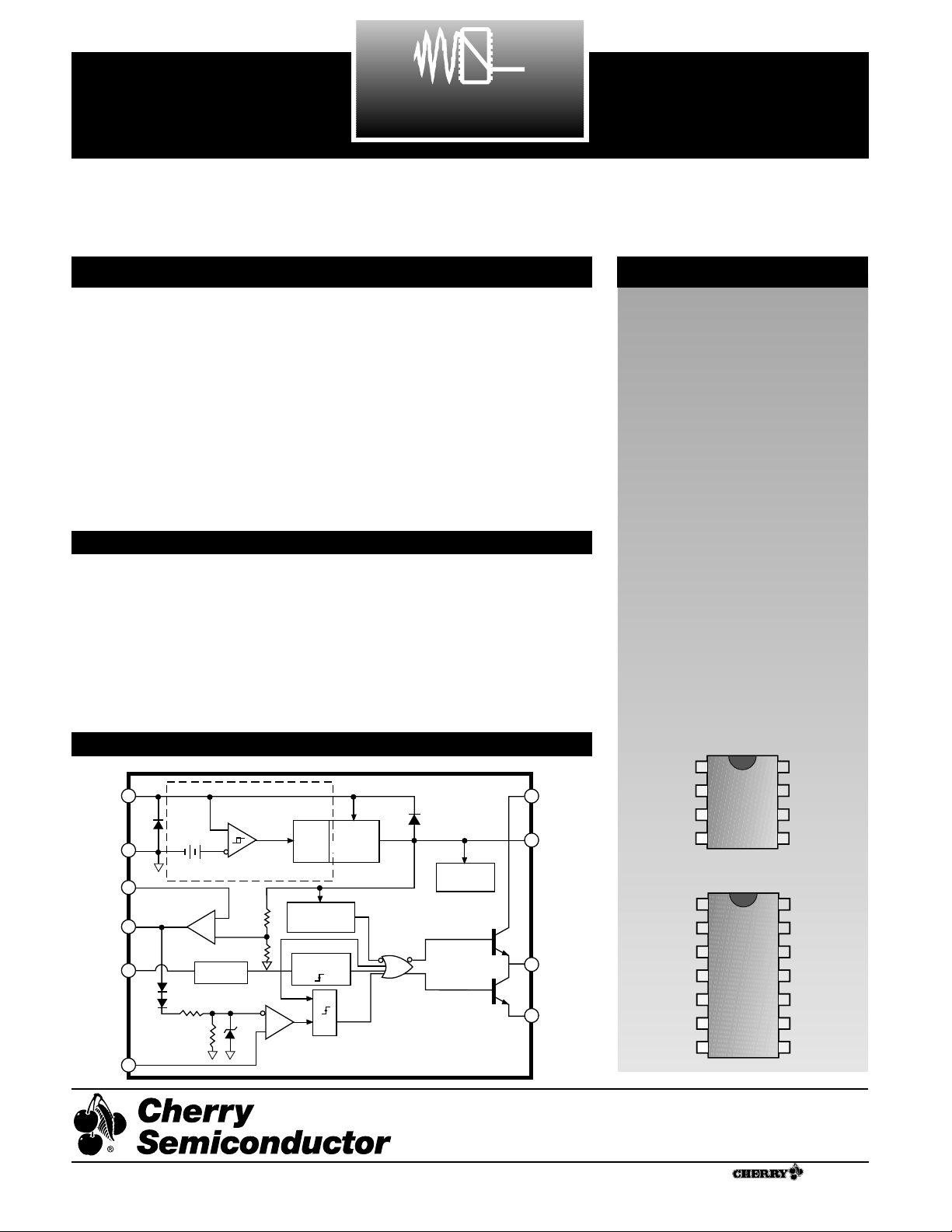
Block Diagram
Absolute Maximum Ratings
Supply Voltage (I
CC
<30mA) ..........................................................Self Limiting
Supply Voltage (Low Impedance Source)...................................................30V
Output Current ...............................................................................................±1A
Output Energy (Capacitive Load) .................................................................5µJ
Analog Inputs (V
FB
, V
SENSE
)...........................................................-0.3V to 5.5V
Error Amp Output Sink Current...............................................................10mA
Lead Temperature Soldering
Reflow (SMD styles only)...........60 sec. max above 183°C, 230°C peak
10
7
14
13
12
8
1
2
3
4
5
6
11
9
COMP
NC
V
FB
NC
Sense
NC
OSC
V
REF
NC
V
CC
VCC Pwr
V
OUT
Pwr Gnd
Gnd
14L SO Narrow
7
8
2
3
4
5
6
COMP
V
FB
Sense
OSC
V
REF
V
CC
V
OUT
Gnd
8L SO Narrow
Rev. 3/4/99
Cherry Semiconductor Corporation
2000 South County Trail, East Greenwich, RI 02818
Tel: (401)885-3600 Fax: (401)885-5786
Email: info@cherry-semi.com
Web Site: www.cherry-semi.com
A Company
®
V
Undervoltage Lock-out
V
CC
CC
V
Pwr
CC
1
34V
Gnd
8.4V/7.6V
V
FB
COMP
OSC
Sense
Error
Amplifier
2 R
+
2.50V
Oscillator
R
1V
Undervoltage
R
R
Current
Sensing
Comparator
Set/
Reset
V
REF
Lockout
Toggle
Flip-Flop
S
R
PWM
Latch
5.0 Volt
Reference
NOR
Internal
Bias
V
REF
V
OUT
Pwr Gnd

2
Electrical Characteristics: -40 ≤ TA ≤ 85˚C; V
CC
= 15V (Note 1); RT = 10kΩ; CT = 3.3nF for sawtooth mode.unless otherwise stated.
CS52845
PARAMETER TEST CONDITIONS MIN TYP MAX UNIT
■ Reference Section
Output Voltage TJ=25˚C, I
REF
=1mA 4.95 5.00 5.05 V
Line Regulation 12≤V
CC
≤25V 6 20 mV
Load Regulation 1≤I
REF
≤20mA 6 25 mV
Temperature Stability (Note 2) 0.2 0.4 mV/˚C
Total Output Variation Line, Load, Temp. (Note 2) 4.90 5.10 V
Output Noise Voltage 10Hz≤f≤10kHz, T
J
=25˚C (Note 2) 50 µV
Long Term Stability T
A
=125˚C, 1000 Hrs. (Note 2) 5 25 mV
Output Short Circuit TA=25˚C -30 -100 -180 mA
■ Oscillator Section
Initial Accuracy Sawtooth Mode, T
J
=25˚C475257kHz
Voltage Stability 12≤V
CC
≤25V 0.2 1.0 %
Temperature Stability Sawtooth Mode T
MIN≤TA≤TMAX
(Note 2) 5 %
Amplitude V
OSC
(peak to peak) 1.7 V
■ Error Amp Section
Input Voltage V
COMP
=2.5V 2.45 2.50 2.55 V
Input Bias Current VFB=0V -0.3 -1.0 µA
A
VOL
2≤V
OUT
≤4V 65 90 dB
Unity Gain Bandwidth (Note 2) 0.7 1.0 MHz
PSRR 12≤VCC≤25V 60 70 dB
Output Sink Current VFB=2.7V, V
COMP
=1.1V 2 6 mA
Output Source Current VFB=2.3V, V
COMP
=5V -0.5 -0.8 mA
V
OUT
HIGH VFB=2.3V, RL=15kΩ to Gnd 5 6 V
V
OUT
LOW VFB=2.7V, RL=15kΩ to V
REF
0.7 1.1 V
■ Current Sense Section
Gain (Notes 3 & 4) 2.85 3.00 3.15 V/V
Maximum Input Signal V
COMP
=5V (Note 3) 0.9 1.0 1.1 V
PSRR 12≤V
CC
≤25V (Note 3) 70 dB
Input Bias Current V
Sense
=0V -2 -10 µA
Delay to Output TJ=25˚C (Note 2) 150 300 ns
■ Output Section
Output Low Level I
SINK
=20mA 0.1 0.4 V
I
SINK
=200mA 1.5 2.2 V
Output High Level I
SOURCE
=20mA 13.0 13.5 V
I
SOURCE
=200mA 12.0 13.5 V
Rise Time TJ=25˚C, CL=1nF (Note 2) 50 150 ns
Fall Time TJ=25˚C, CL=1nF (Note 2) 50 150 ns
 Loading...