

Cherry Semiconductor CS5231-3GDPR5, CS5231-3GDP5 Datasheet
Features
CS5231-3
500mA, 3.3V Linear Regulator
with Auxiliary Control
CS5231-3
Description
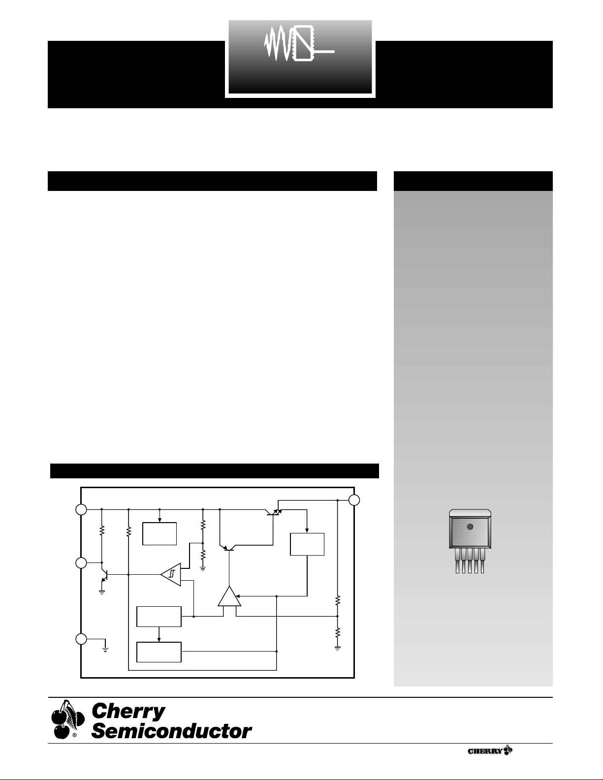
Block Diagram
1
1
1. No Connect
2. V
IN
3. Gnd
4. V
OUT
5. AuxDrv
Tab = Gnd
A Company
®
Rev. 3/31/99
Cherry Semiconductor Corporation
2000 South County Trail, East Greenwich, RI 02818
Tel: (401)885-3600 Fax: (401)885-5786
Email: info@cherry-semi.com
Web Site: www.cherry-semi.com
Consult factory for other package
options.
The CS5231-3 combines a threeterminal linear regulator with circuitry to control an external PFET
transistor with the intent of managing two input supplies. A 5V supply powers the regulator while an
auxiliary 3.3V supply is controlled
by the IC. The design has been optimized to provide a “glitch-free”
transition between the two supplies.
The CS5231-3 linear regulator provides a fixed 3.3V output @ 500mA
with an overall accuracy of ± 2%.
The NPN-PNP composite pass transistor provides a low dropout voltage and requires less supply current than PNP designs. Full protection including current limit and
thermal shutdown is provided.
Also designed for low reverse current, the IC prevents excessive cur-
rent from flowing from the output
to ground if the regulator input
voltage is lower than the output
voltage.
The CS5231-3 also controls an auxiliary supply that can provide power
to the regulator output when input
voltage for the regulator is not
available. The AuxDrv auxiliary
output is normally pulled up to the
regulator input voltage and drives
low whenever the input voltage
drops below 4.4V (nominal). It is
typically used to control a PFET
switch that connects a 3.3V auxiliary supply to the regulator output.
The CS5231-3 is available in a
5-lead D
2
PAK (TO-263) package.
Applications include Network
Interface Cards (NICs), modem
cards and power supplies with
multiple input sources.
Linear Regulator
■ 3.3V ± 2% Output Voltage
■ 3mA Quiescent Current
@ 500mA
■ Fast Transient Response
■ Current Limit
■ Thermal Shutdown with
Hysteresis
■ 450µA Reverse Output
Current
■ Fast Transient Response
System Power Management
■ Auxiliary Supply Control
−
+
−
+
Internal
Bias
Bandgap
Reference
Thermal
Shutdown
Current
Limit
V
IN
10kΩ 50kΩ
AuxDrv
Gnd
V
IN
UV
Comparator
V
REF
Error
Amp
Shutdown
V
OUT
Package Options
5 Lead D2PAK
Electrical Characteristics:
0°C < TA< 70°C, 0°C < TJ< 125°C,
4.75V ≤ V
CC
< 6V, C
OUT
≥ 10µF with ESR < 1Ω,
I
OUT
= 10mA, u
nless otherwise specified.
PARAMETER TEST CONDITIONS MIN TYP MAX UNIT
CS5231-3
2
Absolute Maximum Ratings
Maximum Operating Junction Temperature ..........................................................................................................................150°C
Storage Temperature Range .....................................................................................................................................-65°C to +150°C
Lead Temperature Soldering
Reflow (SMD styles only) ...........................................................................................60 sec. max above 183°C, 230°C peak
ESD Damage Threshold (Human Body Model)....................................................................................................................2kV
PIN SYMBOL PIN NAME
V
MAX
V
MIN
I
SOURCE
I
SINK
V
IN
IC Power Input 14V -0.3V 100mA Internally
Limited
V
OUT
Output Voltage 6V -0.3V Internally 100mA
Limited
AuxDrv Auxiliary Drive Output 14V -0.3V 10mA 50mA
Gnd IC Ground N/A N/A N/A N/A
■ Linear Regulator
Output Voltage 10mA < I
OUT
< 500mA 3.234 3.300 3.366 V
-2% +2%
Line Regulation I
OUT
= 10mA, 1 5 mV
VIN= 4.75V to 6V
Load Regulation VIN= 5V, 5 15 mV
I
OUT
= 10mA to 500mA
Ground Current I
OUT
= 10mA 2 3 mA
I
OUT
= 500mA 3 6 mA
Reverse Current VIN= 0V, V
OUT
= 3.3V 0.45 1 mA
Current Limit 0V < V
OUT
< 3.2V 0.55 0.85 1.2 A
Thermal Shutdown Note 1 150 180 210 °C
Thermal Shutdown Hysteresis Note 1 25 °C
■ Auxiliary Drive
Upper V
IN
Threshold Increase VINuntil regulator turns on 4.35 4.5 4.65 V
and AuxDrv drives high
Lower V
IN
Threshold Decrease VINuntil regulator turns off 4.25 4.4 4.55 V
and AuxDrv drives low
V
IN
Threshold Hysteresis 75 100 125 mV
Output Low Voltage I
AuxDrv
= 100µA, 0.1 0.4 V
1V < V
IN
< 4.5V
Output Low Peak Voltage Increase VINfrom 0V to 1V. 0.65 0.9 V
Record peak AuxDrv output voltage
AuxDrv Current Limit V
AuxDrv
= 1V, 0.5 6 25 mA
VIN= 4.0V
Response Time Step V
IN
from 5V to 4V, measure time 1 10 µs
for V
AuxDrv
to drive low. Note 1
Pull-Up/Down Resistance VIN= 0V and VIN> 4.7V 5 10 25 kΩ
Note 1: Guaranteed by design, not 100% production tested. Thermal shutdown is 100% functionally tested at wafer
probe.
CS5231-3
Package Pin Description
PACKAGE PIN # PIN SYMBOL FUNCTION
3
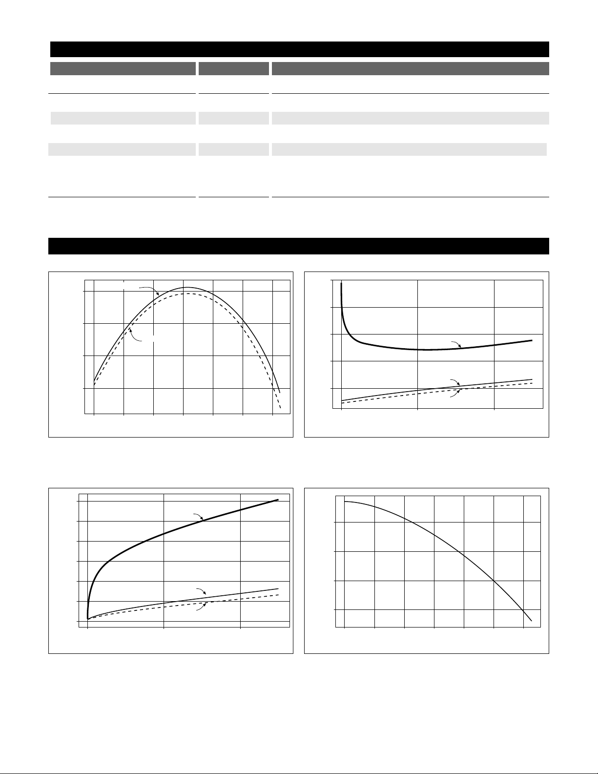
Typical Performance Characteristics
Output Voltage vs. Junction Temperature
Load Regulation (mV)
I
OUT
(A)
1.2
1.0
0.8
0.6
0.4
0.2
0.0
0.0 0.2 0.4
125°C
27°C
0°C
Load Regulation vs. I
OUT
Over Temperature
Line Regulation vs. I
OUT
Over Temperature
Reverse Current (µA)
390
380
370
360
0 20 40 60 80 100 120
Junction Temperature (°C)
Reverse Current vs. Junction Temperature
5Lead D2PAK
1 N/C No connection.
2V
IN
Input voltage.
3 Gnd Ground and IC substrate connection (case).
4V
OUT
Regulated output voltage.
5 AuxDrv Output used to control an auxiliary supply voltage. This lead is
driven low if V
IN
is less than 4.5V, and is otherwise pulled up
to V
IN
through an internal 10kΩ resistor.
Output Voltage (V)
3.302
3.300
3.298
3.296
0 20 40 60 80 100 120
Junction Temperature (°C)
I
OUT
= 10mA
I
OUT
= 500mA
Line Regulation (µV)
I
OUT
(A)
80
70
60
50
40
0.0 0.2 0.4
27°C
0°C
125°C
4.75V <V
IN
< 6V
CS5231-3
4
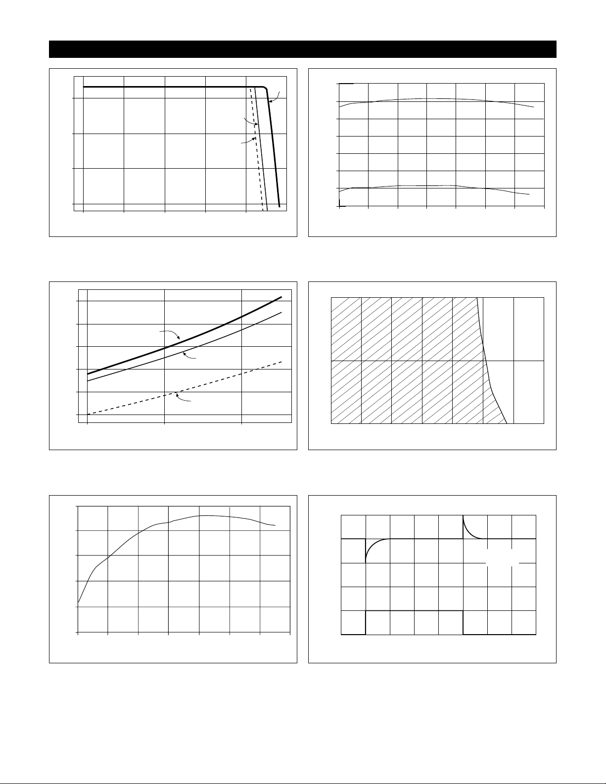
Typical Performance Characteristics: continued
Ground Current (mA)
Load Current (A)
2.6
2.4
2.2
2.0
1.8
1.6
0.0 0.2 0.4
TJ = 0°C
I
Gnd
@ 0°C
TJ = 27°C
I
Gnd
@ 27°C
TJ = 125°C
I
Gnd
@ 125°C
Ground Current vs. Load Current
Temperature (C)
Current Limit (mA)
5.000
4.800
4.600
4.400
4.200
4.000
0
20
40 60 80
100
120
140
AuxDrv Current Limit vs. Junction Temperature
V
OUT
(V)
I
OUT
(A)
3
2
1
0
0.0 0.2 0.4
125°C
27°C
0°C
0.6 0.8 1.0
V
OUT
vs. I
OUT
Over Temperature
V
IN
Threshold Voltage (V)
Junction Temperature (C)
4.520
4.500
4.480
4.460
4.440
4.420
4.400
4.380
0
20
40
60
80
100
120
140
V
IN
Turn-on
Threshold
V
IN
Turn-on
Threshold
VINThresholds vs. Junction Temperature
6.0
5.04.03.02.01.00.0
10
100
1000
7.0
Capacitance (µF)
Capacitance ESR(Ω)
Region of Stable Operation
3.400
3.300
3.200
500mA
10mA
Time, 5µs per division
V
OUT
I
OUT
CIN = 33µF
C
OUT
= 33µF
VIN = 5.00V
Transient Response
 Loading...