

Cherry Semiconductor CS5208-1GT3 Datasheet
1
Features
■ 1.25V to 4.5V V
OUT
at 8A
■ Dropout Voltage < 1.0V @ 8A
■ 1.5% Trimmed Reference
■ Fast Transient Response
■ Thermal Shutdown
■ Current Limit
■ Short Circuit Protection
Package Options
CS5208-1
8A LDO 3-Pin Adjustable Linear Regulator
CS5208-1
Description
The CS5208-1 linear regulator provides 8A at adjustable voltages
from 1.25V to 4.5V. This adjustable
device requires two external resistors to set the output voltage and
provide the minimum load current
for proper regulation.
This regulator is intended for use
as a post regulator and microprocessor supply. The fast loop
response and low dropout voltage
make this regulator ideal for applications where low voltage opera-
tion and good transient response
are important.
The circuit is designed to operate
with dropout voltages as low as
1.0V at 8A.
The regulator is protected against
overload conditions with overcurrent and thermal shutdown
protection circuitry.
The regulator is available in a
TO-220 package.
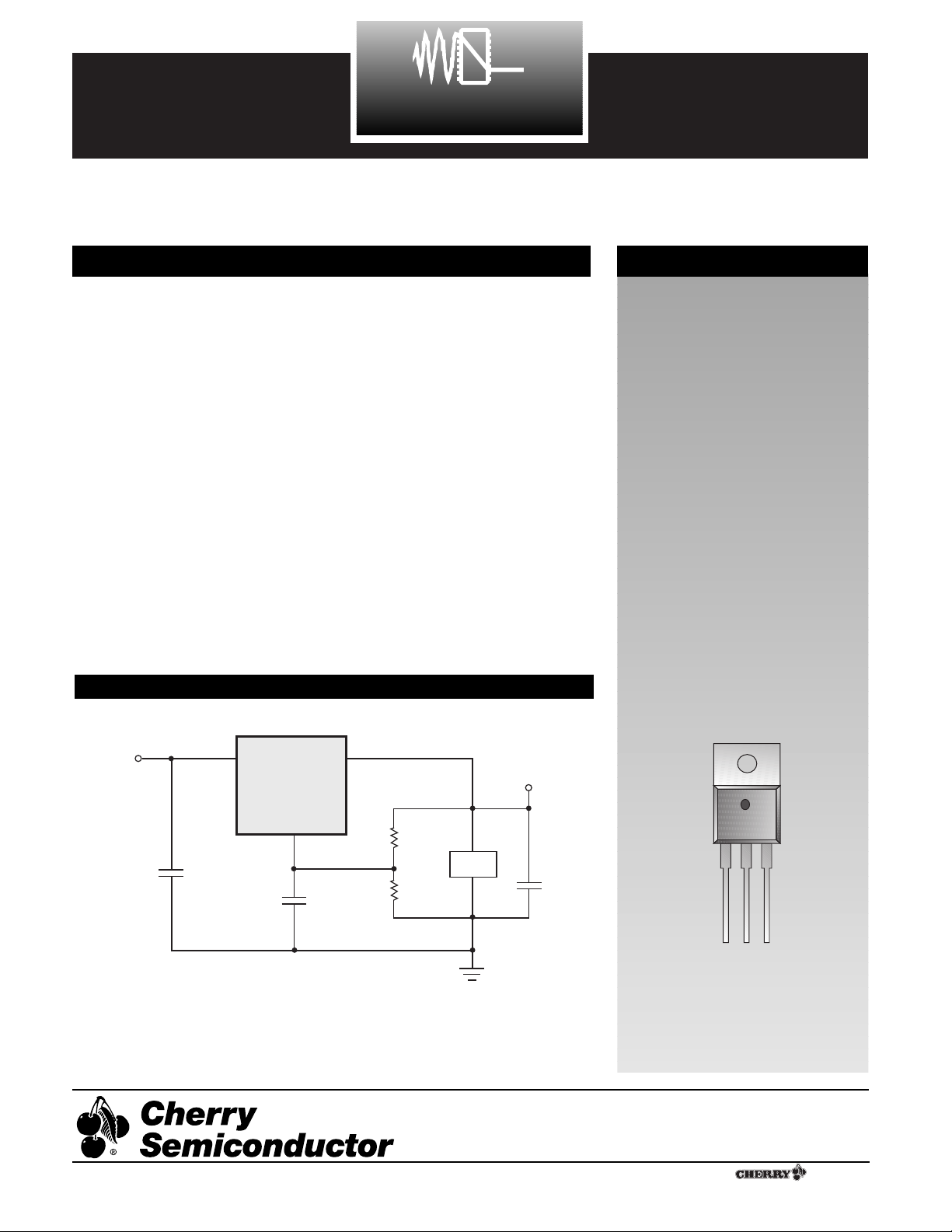
Applications Diagram
1
3 Lead TO-220
1. Adjust
2. V
OUT
3. V
IN
Tab = V
OUT
Cherry Semiconductor Corporation
2000 South County Trail, East Greenwich, RI 02818
Tel: (401)885-3600 Fax: (401)885-5786
Email: info@cherry-semi.com
Web Site: www.cherry-semi.com
A Company
¨
Rev. 6/11/97
5.0V
V
IN
CS5208-1
V
OUT
3.3V @ 8A
100mF
Adj
0.1mF
124
200
Load
300mF
Package Pin Description
PACKAGE PIN # PIN SYMBOL FUNCTION
Electrical Characteristics: 0¡C²TA² 70¡C, 0¡C²TJ² 150¡C, V
Adj
= 0V unless otherwise specified.
PARAMETER TEST CONDITIONS MIN TYP MAX UNIT
CS5208-1
2
Absolute Maximum Ratings
Input Voltage ...............................................................................................................................................................................6V
Operating Junction Temperature Range..........................................................................................................0¡C ² T
J
² 150¡C
Storage Temperature Range ...............................................................................................................................-65¡C to +150¡C
Lead Temperature Soldering: Wave Solder (through hole styles only).........................................10 sec. max, 260¡C peak
ESD Damage Threshold ...........................................................................................................................................................2kV
3L TO-220
1 Adjust This pin is connected to the low side of the internally trimmed 1.5%
bandgap reference voltage and carries a bias current of about 70µA.
A resistor divider from Adj to V
OUT
and from Adj to ground sets
the output voltage. Also, transient response can be improved by
adding a small bypass capacitor from this pin to ground.
2V
OUT
This pin is connected to the emitter of the power pass transistor and
provides a regulated voltage capable of sourcing 8A of current.
3V
IN
This is the supply voltage for the regulator . For the device to regulate, this voltage should be between 1.1V and 1.30V (depending on
the output current) greater than the output voltage.
Reference Voltage VIN=2.75V to 5.5V, I
OUT
=10mA to 8A 1.234 1.253 1.271 V
(-1.5%) (+1.5%)
Line Regulation VIN=2.75V to 5.5V, I
OUT
=10mA .02 .20 %
Load Regulation VIN=2.75V,I
OUT
=10mA to 8A .04 .50 %
Minimum Load Current VIN=5V, ÆV
OUT
= +1.5% 5 10 mA
(Note 1)
Adjust Pin Current VIN=2.75V,I
OUT
=10mA 70 120 µA
Current Limit VIN=2.75V,ÆV
OUT
= -1.5% 8.1 9.0 A
Short Circuit Current VIN=2.75V,V
OUT
=0V 6.0 8.5 A
Ripple Rejection VIN=3.25V Avg, 60 80 dB
(Note 2) V
Ripple
=1V
P-P
@120Hz,
I
OUT
=4A,C
Adj
=0.1µF; C
OUT
= 22µF
Thermal Regulation (Note 2) 30ms Pulse, TA=25¡C 0.002 %/W
Dropout Voltage I
OUT
=100mA 0.92 1.15 V
(Minimum V
IN -VOUT
)I
OUT
=1A 0.93 1.15 V
(Note 3) I
OUT
=2.75A 0.94 1.15 V
I
OUT
=4A 0.95 1.15 V
I
OUT
=8A 0.96 1.30 V
RMS Output Noise Freq=10Hz to 10kHz, TA=25¡C 0.003 %V
OUT
Temperature Stability 0.5 %
Thermal Shutdown (Note 4) 150 180 210 ¡C
Thermal Shutdown Hysteresis 25 ¡C
(Note 4)
Note 1: The minimum load current is the minimum current required to maintain regulation. Normally the current in the resistor
divider used to set the output voltage is selected to meet the minimum load current requirement.
Note 2: This parameter is guaranteed by design and is not 100% production tested.
Note 3: Dropout voltage is defined as the minimum input/output voltage differential required to maintain 1.5% regulation.
Note 4: This parameter is guaranteed by design, but not parametrically tested in production. However, a 100% thermal shutdown
functional test is performed on each part.
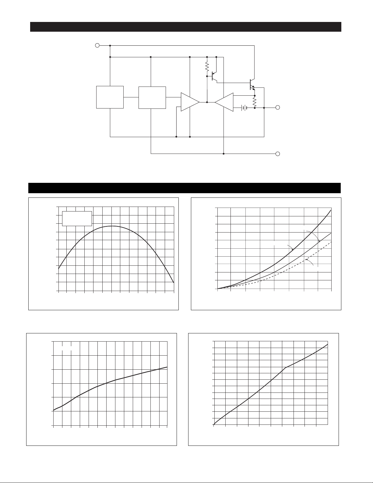
Block Diagram
CS5208-1
3
Typical Performance Characteristics
0 10 20 30 40 50 60 70 80 90 100 110 120 130
-0.150
-0.125
-0.100
-0.075
-0.050
-0.025
-0.000
0.025
0.050
0.075
0.100
TJ (°C)
Output Voltage Deviation (%)
IO=10mA
V
IN
=2.75V
Output Voltage Deviation (%)
Output Current (A)
T
Case
=0°C
T
Case
=25°C
T
Case
=125°C
0.00
8.00
0.000
0.200
0.225
0.250
0.175
0.150
0.125
0.100
0.075
0.050
0.025
1.00 2.00 3.00 4.00 5.00 6.00
7.00
0 10 20 30 40 50 60 70 80 90 100 110 120 130
60.00
65.00
70.00
75.00
80.00
85.00
90.00
T
Case
(°C)
Adjust Pin Current (mA)
IO=10mA
Reference Voltage vs. Temperature
Load Regulation vs. Output Current
Adjust Pin Current vs Temperature
72.4
72.2
72.0
71.8
71.6
71.4
71.2
71.0
70.8
70.6
70.4
0.0 0.8
1.6 3.2 4.0
5.6
6.4 7.2
I
OUT
(A)
Adjust Pin Current (mA)
70.2
70.0
72.6
2.4 4.8 8.0
Adjust Pin Current vs. I
OUT
V
IN
BIAS
and
TSD
V
REF
-
EA
+
IA
+
-
V
OUT
Adj
 Loading...