

Cherry Semiconductor CS5206-3GT3, CS5206-3GDPR3, CS5206-3GDP3, CS5206-1GT3, CS5206-1GDPR3 Datasheet
...
1
Features
■ Output Current to 6A
■ Output Trimmed to +/- 1%
■ Dropout Voltage
1.3V @ 6A
■ Fast Transient Response
■ Fault Protection Circuitry
Thermal Shutdown
Overcurrent Protection
Safe Area Protection
Package Options
3L TO-220
Tab (V
OUT
)
CS5206 -1,-3,-5
6A Adjustable, and Fixed 3.3V
and 5V Linear Regulators
1
CS5206 -1,-3,-5
The CS5206 -X series of linear regulators provides 6A at adjustable
and fixed voltages of 3.3V and 5V
with an accuracy of ±1% and ±2%
respectively. The adjustable version
uses two external resistors to set
the output voltage within a 1.25V
to 13V range.
The regulators are intended for use
as post regulators and microprocessor supplies. The fast loop response
and low dropout voltage make
these regulators ideal for applications where low voltage operation
and good transient response are
important.
The circuit is designed to operate
with dropout voltages as low as 1V
depending on the output current
level. The maximum quiescent current is only 10mA at full load.
The regulators are fully protected
against overload conditions with
protection circuitry for Safe
Operating Area (SOA), overcurrent
and thermal shutdown.
The regulators are available in TO220 and surface mount D2packages.
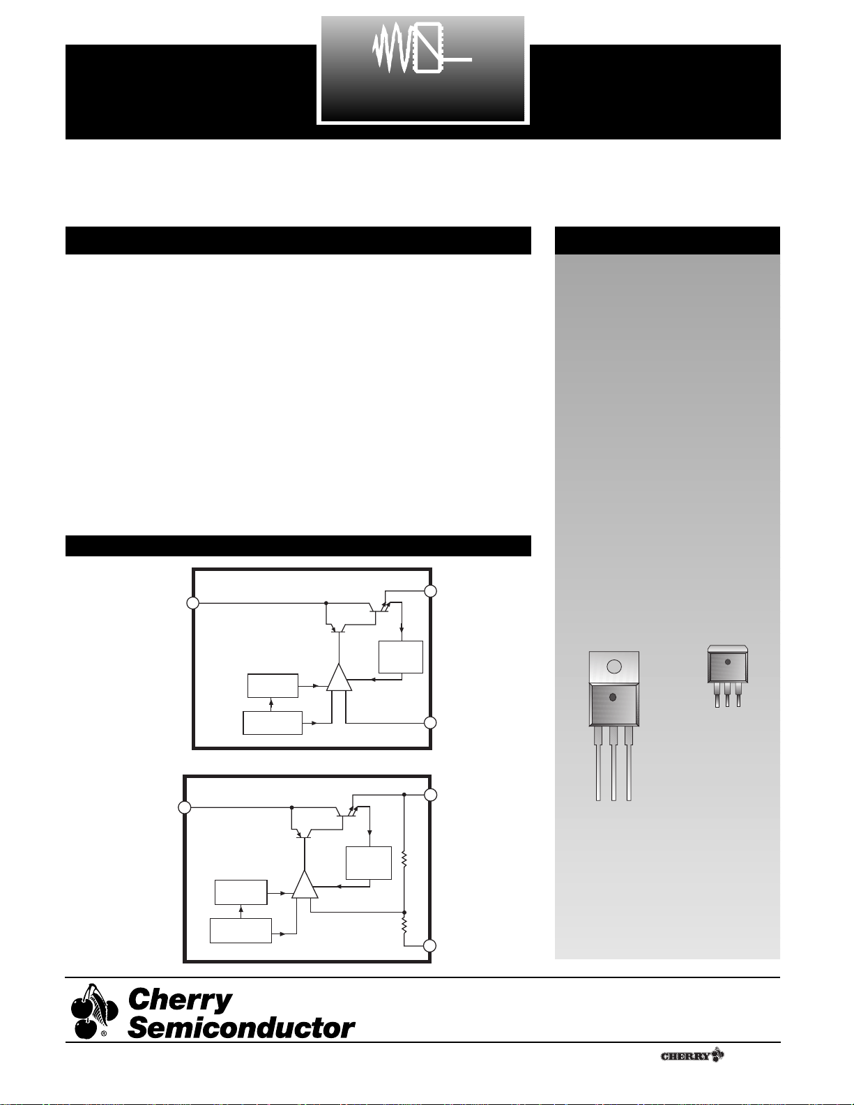
Block Diagram
CS5206 -3, -5
1 Gnd
2V
OUT
3V
IN
CS5206 -1
1 Adj
2V
OUT
3V
IN
CS5206 -1
CS5206 -3, -5
Description
3L D2PAK
1
Rev. 7/8/97
Cherry Semiconductor Corporation
2000 South County Trail, East Greenwich, RI 02818
Tel: (401)885-3600 Fax: (401)885-5786
Email: info@cherry-semi.com
Web Site: www.cherry-semi.com
A Company
¨
V
IN
Output
Current
Limit
Thermal
Shutdown
Bandgap
+
-
Error
Amplifier
V
Adj
OUT
V
Gnd
OUT
V
IN
Output
Current
Limit
Thermal
Shutdown
Bandgap
+
-
Error
Amplifier
2
Electrical Characteristics: C
IN
= 10µF, C
OUT
= 22µF Tantalum, V
IN
Ð V
OUT
=3V, VIN² 10V, 0¡C ² TA ² 70¡C, TJ² +150¡C,
unless otherwise specified, I
full load
= 6A.
PARAMETER TEST CONDITIONS MIN TYP MAX UNIT
CS5206 -1,-3,-5
Absolute Maximum Ratings
Supply Voltage, V
CC
..................................................................................................................................................................17V
Operating Temperature Range................................................................................................................................-40¡C to 70¡C
Junction Temperature ............................................................................................................................................................150¡C
Storage Temperature Range ..................................................................................................................................-60¡C to 150¡C
Lead Temperature Soldering: Wave Solder (through hole styles only)..........................................10 sec. max, 260¡C peak
Reflow (SMD styles only) ......................................................................................60 sec. max above 183¡C, 230¡C peak
Electrical Characteristics: C
IN
= 10µF, C
OUT
= 22µF Tantalum, V
IN
Ð V
OUT
=3V, VIN² 15V, 0¡C ² TA ² 70¡C, TJ² +150¡C,
unless otherwise specified, I
full load
= 6A.
PARAMETER TEST CONDITIONS MIN TYP MAX UNIT
■ Fixed Output Voltage (CS5206 -3, -5)
CS5206 -5 VINÐV
OUT
= 1.5V; 4.9 5.0 5.1 V
(Notes 1 and 2) 0²I
OU T
²6A (-2%) (+2%)
CS5206 -3 VINÐV
OUT
= 1.5V; 3.234 3.300 3.366 V
(Notes 1 and 2) 0²I
OUT
²6A (-2%) (+2%)
Line Regulation 1.5V²VINÐV
OUT
² 6V; I
OUT
=10mA 0.04 0.20 %
Load Regulation VINÐV
OUT
= 1.5V; 0.1 0.4 %
(Notes 1 and 2) 10mA ² I
OUT
²6A
Dropout Voltage (Note 3) I
OUT
=6A 1.3 1.4 V
Current Limit VINÐV
OUT
=3V; TJ³ 25¡C 6.5 8.5 A
VINÐV
OUT
=9V 1.0 A
Quiescent Current VIN²9V; I
OUT
=10mA 5.0 10.0 mA
Thermal Regulation 30ms pulse; TA=25¡C 0.003 %/W
Ripple Rejection f=120Hz; I
OUT
=6A 75 dB
Temperature Stability 0.5 %
■ Adjustable Output Voltage (CS5206 -1)
Reference Voltage VINÐV
OUT
= 1.5V; V
Adj
= 0V 1.241 1.254 1.266 V
(Notes 1 and 2) 10mA²I
OUT
²6A (-1%) (+1%)
Line Regulation 1.5V²VINÐV
OUT
²6V; I
OUT
=10mA 0.04 0.20 %
Load Regulation VINÐV
OUT
=1.5V; 0.1 0.4 %
(Notes 1 and 2) 10mA²I
OUT
²6A
Dropout Voltage (Note 3) I
OUT
=6A 1.3 1.4 V
Current Limit VINÐV
OUT
=3V; TJ³ 25¡C 6.5 8.5 A
VINÐV
OUT
=9V 1.0 A
Minimum Load Current VINÐV
OUT
=7V 1.2 6 mA
Adjust Pin Current 50 100 µA
Adjust Pin Current Change 1.5V²VINÐV
OUT
²4V; 0.2 5.0 µA
10mA²I
OUT
²6A
Thermal Regulation 30ms pulse; TA=25¡C 0.003 %W
Ripple Rejection f=120Hz; C
Adj
=25µF; I
OUT
=6A 82 dB
Temperature Stability 0.5 %
RMS Output Noise 10Hz²f²10kHz; TA=25¡C 0.003 %V
OUT
Thermal Shutdown 150 180 ¡C
Thermal Shutdown Hysteresis 25 ¡C
CS5206 -1,-3,-5
3
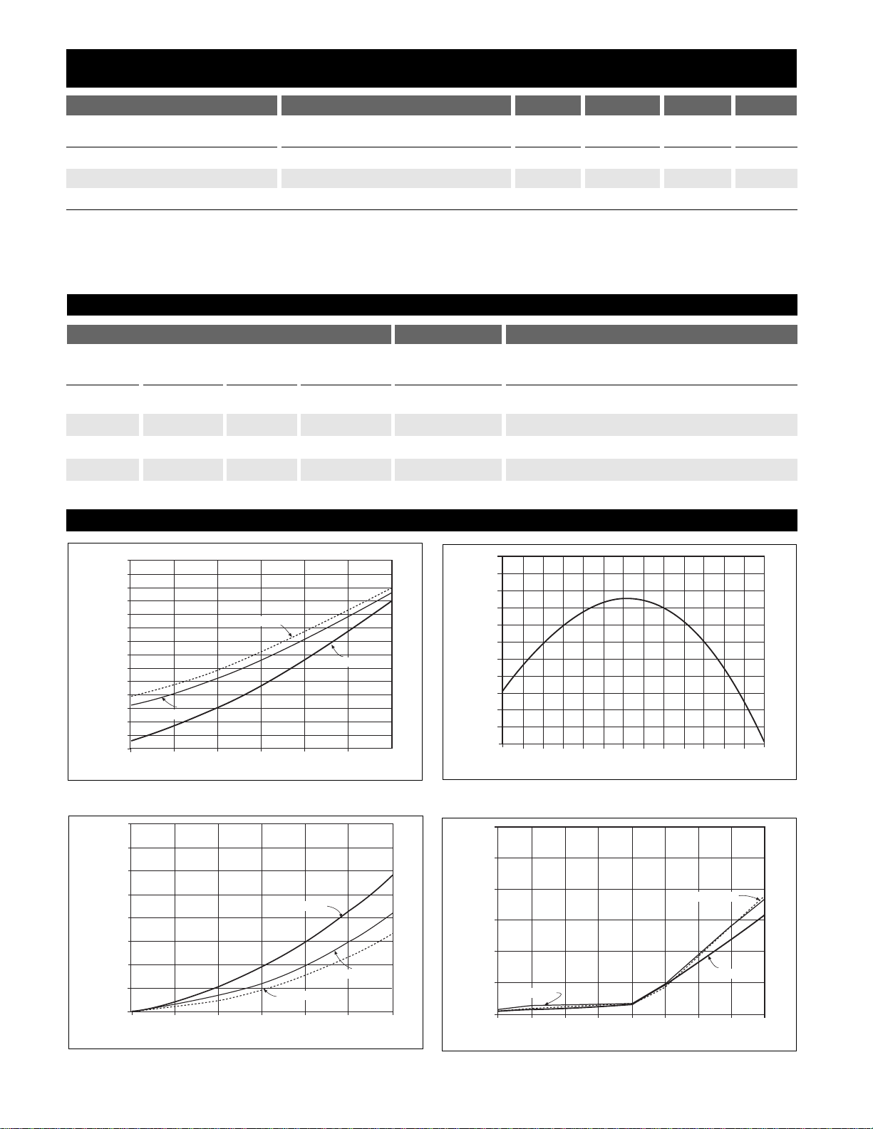
Typical Performance Characteristics
Dropout Voltage vs. Output Current Reference Voltage vs. Temperature
Load Regulation vs. Output Current
Package Pin Description
PACKAGE PIN # PIN SYMBOL FUNCTION
PARAMETER TEST CONDITIONS MIN TYP MAX UNIT
■ Fixed Output Voltage (CS5206 -3, -5)
RMS Output Noise (%V
OUT
) 10Hz²f²10kHz 0.003 %V
OUT
Thermal Shutdown 150 180 ¡C
Thermal Shutdown Hysteresis 25 ¡C
Note 1: Load regulation and output voltage are measured at a constant junction temperature by low duty cycle pulse testing. Changes in out-
put voltage due to thermal gradients or temperature changes must be taken into account separately.
Note 2: Specifications apply for an external Kelvin sense connection at a point on the output pin 1/4Ó from the bottom of the package.
Note 3: Dropout voltage is a measurement of the minimum input/output differential at full load.
Electrical Characteristics: C
IN
= 10µF, C
OUT
= 22µF Tantalum, V
IN
Ð V
OUT
=3V, VIN² 10V, 0¡C ² TA ² 70¡C, TJ² +150¡C,
unless otherwise specified, I
full load
= 6A.
CS5206 -1 CS5206 -3, -5
D2PAK 3L TO-220 D2PAK 3L TO-220
1 1 N/A N/A Adj Adjust pin (low side of the internal reference).
222 2 V
OUT
Regulated output voltage (case).
333 3 VINInput voltage.
N/A N/A 1 1 Gnd Ground connection.
Minimum Load Current
1.40
1.35
1.30
1.25
1.20
1.15
1.10
1.05
1.00
0.95
Dropout Voltage (V)
0.90
0.85
T
= 25°C
CASE
0.80
0.75
0.70
01 2 3 4 5 6
0.200
0.175
0.150
0.125
0.100
0.075
0.050
Output Voltage Deviation (%)
0.025
0.000
01 2 3 4 5 6
T
= 0°C
CASE
Output Current (A)
Output Current (A)
T
= 125°C
CASE
T
= 125°C
CASE
T
= 25°C
CASE
T
= 0°C
CASE
0.10
0.08
0.06
0.04
0.02
0.00
-0.02
-0.04
-0.06
Output Voltage Deviation (%)
-0.08
-0.10
-0.12
0 10 130
20 30 40 50 60 70 80 90 100 110 120
2.500
2.175
1.850
1.525
1.200
Minimum Load Current (mA)
0.875
T
= 25°C
CASE
0.550
123456
VIN – V
TJ (°C)
OUT
(V)
T
CASE
7
T
= 0°C
CASE
= 125°C
8
9
 Loading...