

Cherry Semiconductor CS5203-3GDPR3, CS5203-3GDP3 Datasheet
1
Features
■ Output Current to 3A
■ Output Accuracy to ±1.5%
Over Temperature
■ Dropout Voltage (typical)
1.15V @ 3A
■ Fast Transient Response
■
Fault Protection
Current Limit
Thermal Shutdown
Package Options
CS5203-3
3A, 3.3V Fixed Linear Regulator
CS5203-3
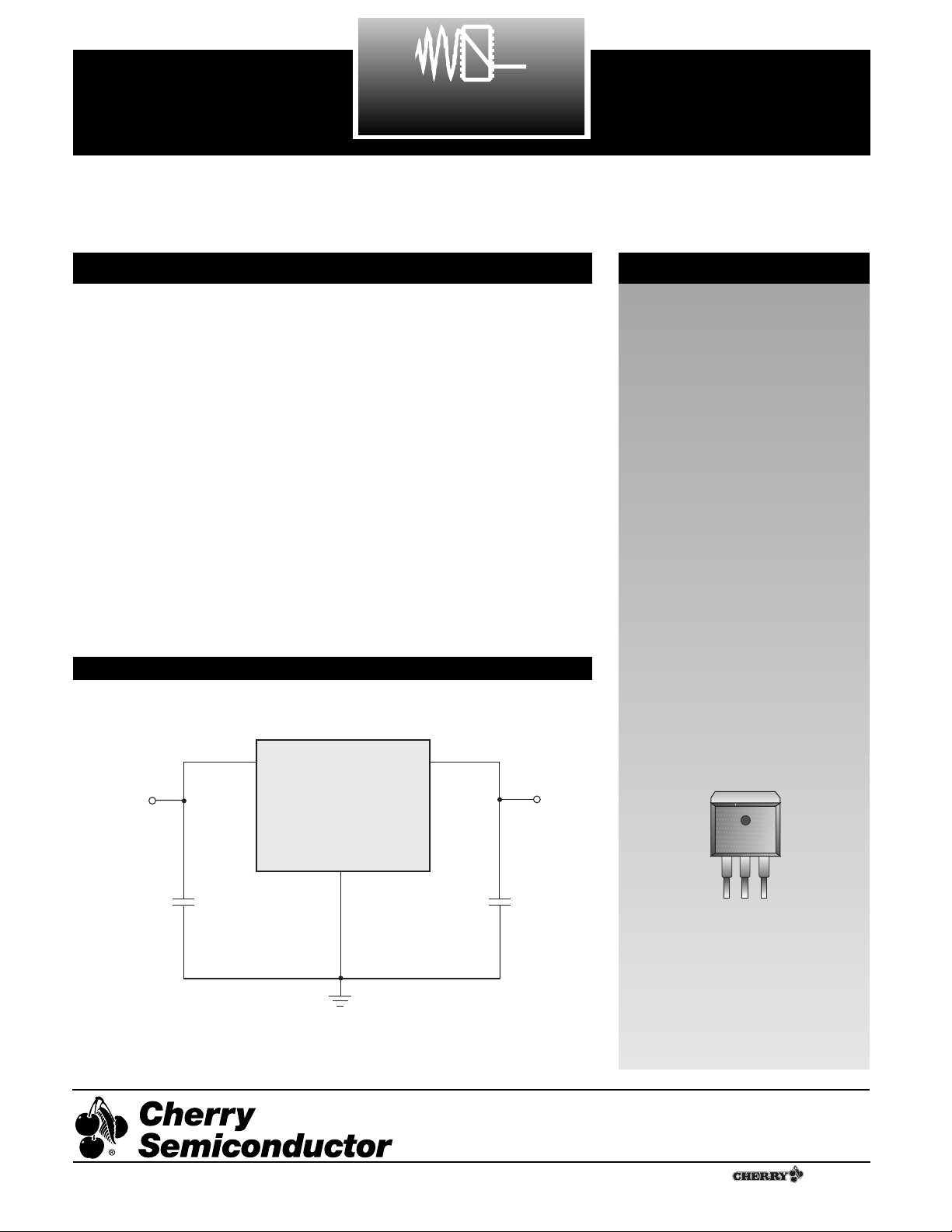
Application Diagram
CS5203 -3
1 Gnd
2V
OUT (Tab)
3V
IN
Description
3L D2PAK
Tab (V
OUT
)
1
Consult factory for other package
options.
The CS5203-3 linear regulator
provides a 3.3V reference at 3A
with an output voltage accuracy
of ±1.5%.
This regulator is intended for
use as a post regulator and
microprocessor supply. The fast
loop response and low dropout
voltage make this regulator
ideal for applications where low
voltage operation and good
transient response are important.
The circuit is designed to provide 3A of output current with
dropout voltages of less than
1.15V. The maximum quiescent
current is only 10mA at full
load. Device protection includes
overcurrent and thermal shutdown.
The CS5203-3 is pin compatible
with the LT1085 family of linear
regulators.
The regulator is available in a
surface mount D
2
package.
Rev. 6/3/98
Cherry Semiconductor Corporation
2000 South County Trail, East Greenwich, RI 02818
Tel: (401)885-3600 Fax: (401)885-5786
Email: info@cherry-semi.com
Web Site: www.cherry-semi.com
A Company
¨
V
IN
5V
V
OUT
CS5203-3
3.3V
@ 3A
100mF
5V
GND
10mF
5V
D2PAK
1 Gnd Ground connection.
2V
OUT
Regulated output voltage (case).
3V
IN
Input voltage.
CS5203-3
Package Pin Description
PACKAGE PIN # PIN SYMBOL FUNCTION
PARAMETER TEST CONDITIONS MIN TYP MAX UNIT
Electrical Characteristics: C
IN
= 10µF, C
OUT
= 22µF Tantalum, V
OUT
+ V
DROPOUT
< VIN< 7V, 0¡C ² TA ² 70¡C, TJ² +150¡C,
unless otherwise specified, I
full load
= 3A.
2
Absolute Maximum Ratings
Supply Voltage, V
IN
. . . . . . . . . . . . . . . . . . . . . . . . . . . . . . . . . . . . . . . . . . . . . . . . . . . . . . . . . . . . . . . . . . . . . . . . . . . . . . . . . . .7V
Operating Temperature Range . . . . . . . . . . . . . . . . . . . . . . . . . . . . . . . . . . . . . . . . . . . . . . . . . . . . . . . . . . . . . . . .-40¡C to 70¡C
Junction Temperature . . . . . . . . . . . . . . . . . . . . . . . . . . . . . . . . . . . . . . . . . . . . . . . . . . . . . . . . . . . . . . . . . . . . . . . . . . . . . . .150¡C
Storage Temperature Range . . . . . . . . . . . . . . . . . . . . . . . . . . . . . . . . . . . . . . . . . . . . . . . . . . . . . . . . . . . . . . . . . .-60¡C to 150¡C
Lead Temperature Soldering
Reflow (SMD styles only) . . . . . . . . . . . . . . . . . . . . . . . . . . . . . . . . . . . . . . . . . . . .60 sec. max above 183¡C, 230¡C peak
ESD Damage Threshold (Human Body Model) . . . . . . . . . . . . . . . . . . . . . . . . . . . . . . . . . . . . . . . . . . . . . . . . . . . . . . . . . .2kV
■ Fixed Output Voltage
Output Voltage VINÐV
OUT
=1.5V; 3.250 3.300 3.350 V
(Notes 1 and 2) 0²I
OUT
²3A (-1.5%) (+1.5%)
Line Regulation 2V²VINÐV
OUT
²3.7V; I
OUT
=10mA 0.02 0.20 %
Load Regulation VINÐV
OUT
=2V; 10mA²I
OUT
²3A 0.04 0.4 %
(Notes 1 and 2)
Dropout Voltage (Note 3) I
OUT
=3A 1.15 1.4 V
Current Limit VINÐV
OUT
=3V 3.1 4.6 A
Quiescent Current I
OUT
=10mA 6.0 10.0 mA
Thermal Regulation (Note 4) 30ms pulse; TA=25¡C 0.002 0.020 %/W
Ripple Rejection (Note 4) f=120Hz; I
OUT
=3A; VINÐV
OUT
=3V; 80 dB
V
RIPPLE
=1V
PP
Thermal Shutdown (Note 5) 150 180 210 ¡C
Thermal Shutdown Hysteresis 25 ¡C
(Note 5)
Note 1: Load regulation and output voltage are measured at a constant junction temperature by low duty cycle pulse testing. Changes in output
voltage due to temperature changes must be taken into account separately.
Note 2: Specifications apply for an external Kelvin sense connection at a point on the output pin 1/4Ó from the bottom of the package.
Note 3: Dropout voltage is a measurement of the minimum input/output differential at full load.
Note 4: Guaranteed by design, not tested in production.
Note 5: Thermal shutdown is 100% functionally tested in production.
 Loading...