

Cherry Semiconductor CS52015-1GT3, CS52015-1GSTR3, CS52015-1GST3, CS52015-1GDPR3, CS52015-1GDP3 Datasheet
Cherry Semiconductor Corporation
2000 South County Trail, East Greenwich, RI 02818
Tel: (401)885-3600 Fax: (401)885-5786
Email: info@cherry-semi.com
Web Site: www.cherry-semi.com
1
Features
■ Output Current to 1.5A
■ Output Accuracy to ±1%
Over Temperature
■ Dropout Voltage (typical)
1.05V @ 1.5A
■ Fast Transient Response
■ Fault Protection
Current Limit
Thermal Shutdown
Package Options
3L TO-220
Tab (V
OUT
)
CS52015-1
1.5A Adjustable Linear Regulator
1
CS52015-1
The CS52015-1 linear regulator provides 1.5A with an accuracy of ±1%.
The device uses two external resistors to set the output voltage within
a 1.25V to 5.5V range.
The regulator is intended for use as
a post regulator and microprocessor
supply. The fast loop response and
low dropout voltage make this regulator ideal for applications where
low voltage operation and good
transient response are important.
The circuit is designed to operate
with dropout voltages less than
1.4V at 1.5A output current. Device
protection includes overcurrent and
thermal shutdown.
The CS52015-1 is pin compatible
with the LT1086 family of linear
regulators but has lower dropout
voltage.
The regulator is available in TO220, surface mount D2, and SOT-223
packages.
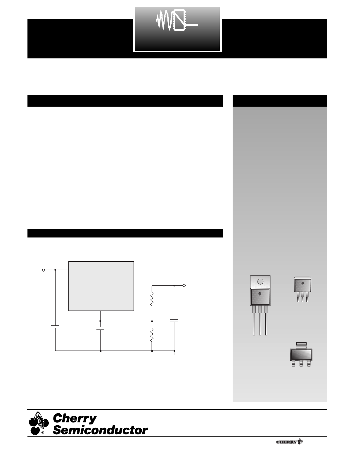
Application Diagram
Consult factory for fixed output voltage
versions.
CS52015 -1
1 Adj
2V
OUT (Tab)
3V
IN
Description
3L D2PAK
Tab (V
OUT
)
1
A Company
¨
SOT-223
Tab (V
OUT
)
1
Rev. 2/17/98
5.0V
V
IN
CS52015-1
V
OUT
3.3V @ 1.5A
10 mF
5V
Adj
0.1mF
5V
Tantalum
124W
1%
200W
1%
22mF
5V
2
CS52015-1
Absolute Maximum Ratings
Supply Voltage, V
CC
....................................................................................................................................................................7V
Operating Temperature Range................................................................................................................................-40¡C to 70¡C
Junction Temperature ............................................................................................................................................................150¡C
Storage Temperature Range ..................................................................................................................................-60¡C to 150¡C
Lead Temperature Soldering
Wave Solder (through hole styles only) .....................................................................................10 sec. max, 260¡C peak
Reflow (SMD styles only) ......................................................................................60 sec. max above 183¡C, 230¡C peak
ESD Damage Threshold............................................................................................................................................................2kV
PACKAGE PIN # PIN SYMBOL FUNCTION
PARAMETER TEST CONDITIONS MIN TYP MAX UNIT
Electrical Characteristics: C
IN
= 10µF, C
OUT
= 22µF Tantalum, V
OUT
+ V
DROPOUT
< VIN< 7V, 0¡C ² TA ² 70¡C, TJ² +150¡C,
unless otherwise specified, I
full load
= 1.5A.
Package Pin Description
■ Adjustable Output Voltage (CS52015-1)
Reference Voltage V
INÐVOUT
=1.5V; V
Adj
= 0V 1.241 1.254 1.266 V
(Notes 1 and 2) 10mA²I
OUT
²1.5A (-1%) (+1%)
Line Regulation 1.5V²VINÐV
OUT
²5.75V; I
OUT
=10mA 0.02 0.20 %
Load Regulation VINÐV
OUT
=1.5V; 10mA²I
OUT
²1.5A 0.04 0.4 %
(Notes 1 and 2)
Dropout Voltage (Note 3) I
OUT
=1.5A 1.05 1.4 V
Current Limit VINÐV
OUT
=3V; TJ³ 25¡C 1.6 3.1 A
Minimum Load Current (Note 4) VIN=7V ; V
Adj
=0 0.6 2.0 mA
Adjust Pin Current VINÐV
OUT
=3V; I
OUT
=10mA 50 100 µA
Thermal Regulation (Note 5) 30ms pulse; TA=25¡C 0.002 0.020 %/W
Ripple Rejection (Note 5) f=120Hz; I
OUT
=1.5A; VINÐV
OUT
=3V; 80 dB
V
RIPPLE
=1V
PP
Thermal Shutdown (Note 6) 150 180 210 ¡C
Thermal Shutdown Hysteresis 25 ¡C
(Note 6)
Note 1: Load regulation and output voltage are measured at a constant junction temperature by low duty cycle pulse testing. Changes in out-
put voltage due to temperature changes must be taken into account separately.
Note 2: Specifications apply for an external Kelvin sense connection at a point on the output pin 1/4Ó from the bottom of the package.
Note 3: Dropout voltage is a measurement of the minimum input/output differential at full load.
Note 4: The minimum load current is the minimum current required to maintain regulation. Normally the current in the resistor divider used
to set the output voltage is selected to meet the minimum requirement.
Note 5: Guaranteed by design, not 100% tested in production.
Note 6: Thermal shutdown is 100% functionally tested in production.
D2PAK TO-220 SOT-223
1 1 1 Adj Adjust pin (low side of the internal reference.
222V
OUT
Regulated output voltage (case).
333VINInput voltage
CS52015-1
3
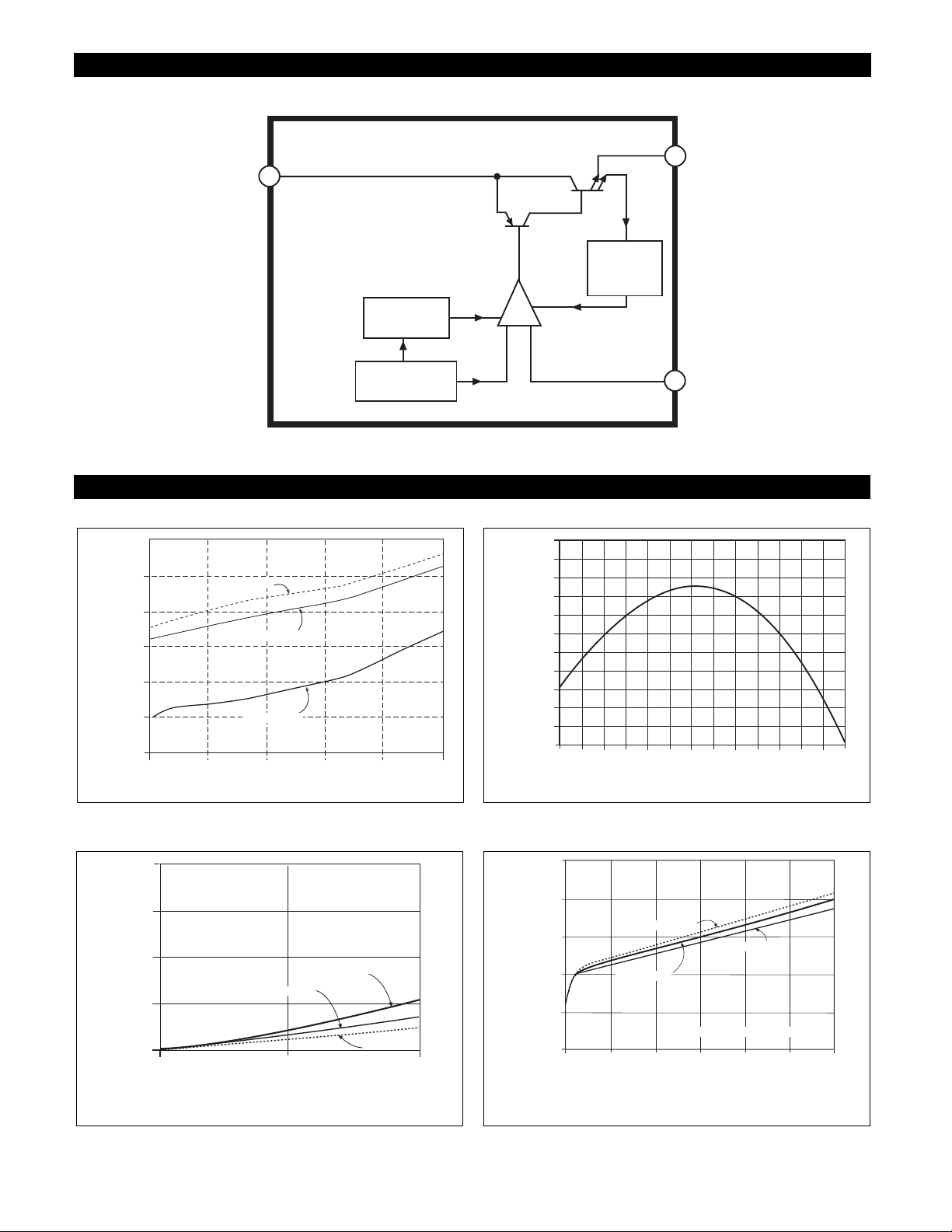
Block Diagram
Dropout Voltage vs. Output Current Reference Voltage vs. Temperature
Load Regulation vs. Output Current
Minimum Load Current vs VIN-V
OUT
Typical Performance Characteristics
V
OUT
V
IN
Output
Current
Limit
Thermal
Shutdown
-
+
Error
Amplifier
1.05
1.00
0.95
0.90
V Drop Out (V)
0.85
0.80
0.75
T
CASE
T
T
0ûC
CASE
CASE
25ûC
125ûC
I
OUT
Bandgap
150012009006003000
(mA)
Adj
0.10
0.08
0.06
0.04
0.02
0.00
-0.02
-0.04
-0.06
Output Voltage Deviation (%)
-0.08
-0.10
-0.12
0 10 130
20 30 40 50 60 70 80 90 100 110 120
TJ (°C)
0.100
0.075
0.050
T
= 25°C
0.025
Output Voltage Deviation (%)
0.000
012
CASE
Output Current (A)
T
CASE
= 125°C
T
CASE
= 0°C
0.65
0.60
T
CASE
T
= 25°C
0.55
0.50
Minimum Load Current (mA)
0.45
0.40
123456
CASE
= 0°C
VIN – V
OUT
T
C
IN =COUT
(V)
= 125°C
CASE
=22mF Tantalum
7
 Loading...