

Cherry Semiconductor CS5166HGDWR16, CS5166HGDW16 Datasheet
Features
■
V
2
TM
Control Topology
■
Dual N-Channel Design
■
125ns Controller Transient Response
■
Excess of 1Mhz Operation
■
5-bit DAC with 1% Tolerance
■
Power-Good Output with Internal
Delay
■
Adjustable Hiccup Mode Over
Current Protection
■
Complete Pentium
®
II System
Requires just 21 Components
■
5V and 12V Operation using either
Dual or Single Supplies
■
Adaptive Voltage Positioning
■
Remote Sense Capability
■
Current Sharing Capability
■
V
CC
Monitor
■
Overvoltage Protection (OVP)
■
Programmable Soft Start
■
200ns PWM Blanking
■
65ns FET Non-Overlap
■
40ns Gate Rise and Fall Times
(3.3nF load)
Package Options
CS5166H
5-Bit Synchronous CPU Controller
with Power-Good and Current Limit
CS5166H
Description
The CS5166H is a synchronous
dual NFET Buck Regulator
Controller. It is designed to power the core logic of the latest high
performance CPUs. It uses the
V
2
TM
control method to achieve
the fastest possible transient
response and best overall regulation. It incorporates many additional features required to ensure
the proper operation and protection of the CPU and power system. The CS5166H provides the
industry’s most highly integrated solution, minimizing external
component count, total solution
size, and cost.
The CS5166H is specifically
designed to power Intel’s
Pentium
®
II processor and
includes the following features:
5-bit DAC with 1% tolerance,
Power-Good output, adjustable
hiccup mode over-current protection, V
CC
monitor, Soft Start,
adaptive voltage positioning,
over-voltage protection, remote
sense and current sharing capability.
The CS5166H will operate over a
4.15 to 20V range using either
single or dual input voltage and
is available in a 16 lead wide
body surface mount package.
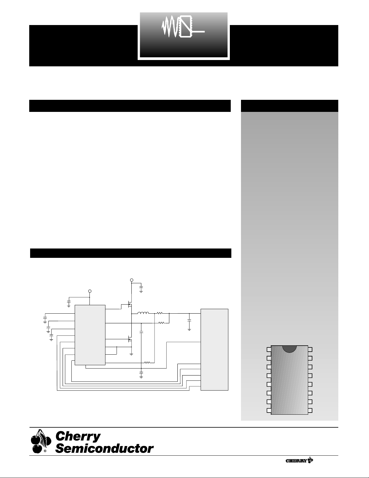
Application Diagram
16 Lead SO WIDE
V
ID0
V
ID1
V
ID2
V
ID3
I
SENSE
C
OFF
SS
V
ID4
V
FB
COMP
LGnd
PWRGD
GATE(L)
PGnd
GATE(H)
V
CC
Pentium is a registered trademark of Intel Corporation.
5V to 2.8V @ 14.2A for 300MHz Pentium® II
1
V2is a trademark of Switch Power, Inc.
Rev. 6/28/99
Cherry Semiconductor Corporation
2000 South County Trail, East Greenwich, RI 02818
Tel: (401)885-3600 Fax: (401)885-5786
Email: info@cherry-semi.com
Web Site: www.cherry-semi.com
A Company
®
12V
1µF
C
OFF
330pF
0.1µF
0.1µF
SS
COMP
V
ID0
V
ID1
V
ID2
V
ID3
V
ID4
V
CS5166H
PWRGD
CC
GATE(H)
I
SENSE
GATE(L)
PGnd
LGnd
V
FB
5V
1200µF/10V x 3
1.2µH
3.0mΩ
1200µF
510
10V x 5
V
V
V
V
V
ID4
ID3
ID2
ID1
ID0
Pentium® II
System
0.1µF
PWRGD
3.3K
1000pF
1

Absolute Maximum Ratings
Pin Symbol Pin Name
V
MAX
V
MIN
I
SOURCE
I
SINK
2
PACKAGE PIN # PIN SYMBOL FUNCTION
Package Pin Description
CS5166H
V
CC
IC Power Input 20V -0.3V N/A 1.5A Peak 200mA DC
SS Soft Start Capacitor 6V -0.3V 200µA 10µA
COMP Compensation Capacitor 6V -0.3V 10mA 1mA
V
FB
Voltage Feedback and Current 6V -0.3V 1mA 1mA
Sense Comparator Input
C
OFF
Off-Time Capacitor 6V -0.3V 1mA 50mA
V
ID0-4
Voltage ID DAC Inputs 6V -0.3V 1mA 10µA
GATE(H) High-Side FET Driver 20V -0.3V 1.5A Peak 1.5A Peak
200mA DC 200mA DC
GATE(L) Low-Side FET Driver 20V -0.3V 1.5A Peak 1.5A Peak
200mA DC 200mA DC
I
SENSE
Current Sense Comparator Input 6V -0.3V 1mA 1mA
PWRGD Power-Good Output 6V -0.3V 10µA 30mA
PGnd Power Ground 0V 0V 1.5A Peak N/A
200mA DC
LGnd Logic Ground 0V 0V 100mA N/A
1,2,3,4,6 V
IDO
– V
ID4
Voltage ID DAC inputs. These pins are internally pulled up to 5V if left
open. V
ID4
selects the DAC range. When V
ID4
is high (logic one), the
Error Amp reference range is 2.125V to 3.525V with 100mV increments.
When V
ID4
is low (logic zero), the Error amp reference voltage is 1.325V
to 2.075V with 50mV increments.
5 SS Soft Start Pin. A capacitor from this pin to LGnd sets the Soft Start and
fault timing.
7C
OFF
Off-Time Capacitor Pin. A capacitor from this pin to LGnd sets both the
normal and extended off time.
8I
SENSE
Current Sense Comparator Inverting Input
9VCCInput Power Supply Pin.
10 GATE(H) High Side Switch FET driver pin.
11 PGnd High Current ground for the GATE(H) and GATE(L) pins.
12 GATE(L) Low Side Synchronous FET driver pin.
13 PWRGD Power-Good Output. Open collector output drives low when VFBis out
of regulation.
14 LGnd Reference ground. All control circuits are referenced to this pin.
15 COMP Error Amp output. PWM Comparator reference input. A capacitor to
LGnd provides Error Amp compensation.
16 V
FB
Error Amp, PWM Comparator feedback input, Current Sense
Comparator Non-Inverting input, and PWRGD comparator input.
Operating Junction Temperature, T
J
. . . . . . . . . . . . . . . . . . . . . . . . . . . . . . . . . . . . . . . . . . . . . . . . . . . . . . . . . . . . . 0° to 150°C
Lead Temperature Soldering:
Reflow (SMD styles only) . . . . . . . . . . . . . . . . . . . . . . . . . . . . . . . . . . . . . . . . . . 60 Sec max. above 183˚C, 230˚C Peak
Storage Temperature Range, TS. . . . . . . . . . . . . . . . . . . . . . . . . . . . . . . . . . . . . . . . . . . . . . . . . . . . . . . . . . . . . . . . -65 to 150˚C

CS5166H
3
Electrical Characteristics: 0˚C < TA< 70˚C; 0˚C < TJ< 125˚C; 8V < VCC< 20V; 2.0V DAC Code (V
ID4
= V
ID3
= V
ID2
=
V
ID1
=0, V
ID0
= 1), C
GATE(H
) = C
GATE(L)
= 3.3nF, C
OFF
= 330pF, CSS= 0.1µF; Unless otherwise stated.
PARAMETER TEST CONDITIONS MIN TYP MAX UNIT
■ VCCSupply Current
Operating 1V<V
FB<VDAC
(Max On-Time),
No Loads on GATE(H) and GATE(L) 12 20 mA
■ V
CC
Monitor
Start Threshold GATE(H) Switching 3.75 3.95 4.15 V
Stop Threshold GATE(H) not switching 3.65 3.87 4.05 V
Hysteresis Start – Stop 80 mV
■ Error Amplifier
V
FB
Bias Current VFB= 0V 0.1 1.0 µA
COMP Source Current COMP = 1.2V to 3.6V; V
FB
= 1.9V 15 30 60 µA
COMP CLAMP Voltage V
FB
= 1.9V, Adjust COMP voltage 0.85 1.0 1.15 V
for Comp current = 60µA
COMP Clamp Current COMP = 0V 0.4 1.0 1.6 mA
COMP Sink Current V
COMP
=1.2V; VFB=2.2V; VSS> 2.5V 180 400 800 µA
Open Loop Gain Note 1 50 60 dB
Unity Gain Bandwidth Note 1 0.5 2 MHz
PSRR @ 1kHZ Note 1 60 85 dB
■ GATE(H) and GATE(L)
High Voltage at 100mA Measure V
CC
–GATE 1.2 2.0 V
Low Voltage at 100mA Measure GATE 1.0 1.5 V
Rise Time 1.6V < GATE < (V
CC
– 2.5V), 40 80 ns
8V < V
CC
< 14V
Fall Time (V
CC
– 2.5V) >GATE > 1.6V, 40 80 ns
8V < V
CC
< 14V
GATE(H) to GATE(L) Delay GATE(H)<2V, GATE(L)>2V
8V < V
CC
< 14V 30 65 100 ns
GATE(L) to GATE(H) Delay GATE(L)<2V, GATE(H)>2V
8V < V
CC
< 14V 30 65 100 ns
GATE pull-down Resistance to PGnd (Note 1) 20 50 115 kΩ
■ Over Current Detection
Current limit voltage V
FB
= 0V to 3.5V 55 76 130 mV
8V < V
CC
< 12V + 10%
I
SENSE
Bias Current I
SENSE
= 2.8V 13 30 50 µA
■ Fault Protection
SS Charge Time V
FB
= 3V, V
ISENSE
= 2.8V 1.6 3.3 5.0 ms
SS Pulse Period V
FB
= 3V, V
ISENSE
= 2.8V 25 100 200 ms
SS Duty Cycle (Charge Time/Period) × 100 1.0 3.3 6.0 %
CS5166H
4
Electrical Characteristics: 0˚C < TA< 70˚C; 0˚C < TJ< 125˚C; 8V < VCC< 20V; 2.0V DAC Code (V
ID4
= V
ID3
= V
ID2
=
V
ID1
=0, V
ID0
= 1), C
GATE(H
) = C
GATE(L)
= 3.3nF, C
OFF
= 330pF, CSS= 0.1µF; Unless otherwise stated.
PARAMETER TEST CONDITIONS MIN TYP MAX UNIT
■ Fault Protection continued
SS Comp Clamp Voltage VFB= 2.7V, VSS= 0V 0.50 0.95 1.10 V
V
FB
Low Comparator Increase VFBtill normal off-time 0.9 1.0 1.1 V
■ PWM Comparator
Transient Response V
FB
= 1.2V to 5V 500ns after GATE(H) 115 175 ns
(after Blanking time) to
GATE(H) = (V
CC
– 1V)
to 1V, 8V < V
CC
< 14V
Minimum Pulse Width Drive V
FB
1.2V to 5V upon GATE(H) 100 200 300 ns
(Blanking Time) rising edge (> V
CC
– 1V), measure
GATE(H) pulse width,
8V < V
CC
< 14V
■ C
OFF
Normal Off-Time VFB= 2.7V 1.0 1.6 2.3 µs
Extended Off-Time V
SS
= VFB= 0V 5.0 8.0 12.0 µs
■ Time-Out Timer
Time-Out Time V
FB
= 2.7V, Measure GATE(H) 10 30 50 µs
Pulse Width
Fault Duty Cycle V
FB
= 0V 30 50 70 %
■ Voltage Identification DAC
Accuracy
(all codes except 11111) Measure V
FB
= COMP, (C
OFF
= Gnd) -1.0 1.0 %
V
ID4VID3VID2VID1VID0
25˚C ≤ TJ ≤ 125˚C, VCC= 12V
1 0 0 0 0 3.489 3.525 3.560 V
1 0 0 0 1 3.390 3.425 3.459 V
1 0 0 1 0 3.291 3.325 3.358 V
1 0 0 1 1 3.192 3.225 3.257 V
1 0 1 0 0 3.093 3.125 3.156 V
1 0 1 0 1 2.994 3.025 3.055 V
1 0 1 1 0 2.895 2.925 2.954 V
1 0 1 1 1 2.796 2.825 2.853 V
1 1 0 0 0 2.697 2.725 2.752 V
1 1 0 0 1 2.598 2.625 2.651 V
1 1 0 1 0 2.499 2.525 2.550 V
1 1 0 1 1 2.400 2.425 2.449 V
1 1 1 0 0 2.301 2.325 2.348 V
1 1 1 0 1 2.202 2.225 2.247 V
1 1 1 1 0 2.103 2.125 2.146 V
0 0 0 0 0 2.054 2.075 2.095 V
0 0 0 0 1 2.004 2.025 2.045 V
0 0 0 1 0 1.955 1.975 1.994 V
0 0 0 1 1 1.905 1.925 1.944 V
CS5166H
5
PARAMETER TEST CONDITIONS MIN TYP MAX UNIT
THRESHOLD ACCURACY
LOWER THRESHOLD UPPER THRESHOLD
MIN TYP MAX MIN TYP MAX UNITS
% of Nominal VIDCode -12 -8.5 -5 5 8.5 12 %
■ DAC CODE
V
ID4VID3VID2VID1VID0
1 0 0 0 0 3.102 3.225 3.348 3.701 3.824 3.948 V
1 0 0 0 1 3.014 3.133 3.253 3.596 3.716 3.836 V
1 0 0 1 0 2.926 3.042 3.158 3.491 3.607 3.724 V
1 0 0 1 1 2.838 2.950 3.063 3.386 3.499 3.612 V
1 0 1 0 0 2.750 2.859 2.968 3.281 3.390 3.500 V
1 0 1 0 1 2.662 2.767 2.873 3.176 3.282 3.388 V
1 0 1 1 0 2.574 2.676 2.778 3.071 3.173 3.276 V
1 0 1 1 1 2.486 2.584 2.683 2.966 3.065 3.164 V
1 1 0 0 0 2.398 2.493 2.588 2.861 2.956 3.052 V
1 1 0 0 1 2.310 2.401 2.493 2.756 2.848 2.940 V
1 1 0 1 0 2.222 2.310 2.398 2.651 2.739 2.828 V
Electrical Characteristics: 0˚C < TA< 70˚C; 0˚C < TJ< 125˚C; 8V < VCC< 20V; 2.0V DAC Code (V
ID4
= V
ID3
= V
ID2
=
V
ID1
=0, V
ID0
= 1), C
GATE(H
) = C
GATE(L)
= 3.3nF, C
OFF
= 330pF, CSS= 0.1µF; Unless otherwise stated.
Accuracy (all codes except 11111) Measure VFB= COMP, (C
OFF
= Gnd) -1.0 1.0 %
V
ID4VID3VID2VID1VID0
0 0 1 0 0 1.856 1.875 1.893 V
0 0 1 0 1 1.806 1.825 1.843 V
0 0 1 1 0 1.757 1.775 1.792 V
0 0 1 1 1 1.707 1.725 1.742 V
0 1 0 0 0 1.658 1.675 1.691 V
0 1 0 0 1 1.608 1.625 1.641 V
0 1 0 1 0 1.559 1.575 1.590 V
0 1 0 1 1 1.509 1.525 1.540 V
0 1 1 0 0 1.460 1.475 1.489 V
0 1 1 0 1 1.410 1.425 1.439 V
0 1 1 1 0 1.361 1.375 1.388 V
0 1 1 1 1 1.311 1.325 1.338 V
1 1 1 1 1 1.219 1.247 1.269 V
Input Threshold V
ID4
, V
ID3
, V
ID2
, V
ID1
, V
ID0
1.0 1.25 2.4 V
Input Pull-up Resistance V
ID4
, V
ID3
, V
ID2
, V
ID1
, V
ID0
25 50 100 kΩ
Input Pull-up Voltage 4.85 5.00 5.15 V
■ Power-Good Output
Low to High Delay V
FB
= (0.8 × V
DAC
) to V
DAC
30 65 110 µs
High to Low Delay V
FB
= V
DAC
to (0.8 × V
DAC
) 30 75 120 µs
Output Low Voltage V
FB
= 2.4V, I
PWRGD
= 500µA 0.2 0.3 V
Sink Current Limit V
FB
= 2.4V, PWRGD = 1V 0.5 4.0 15.0 mA
THRESHOLD ACCURACY
LOWER THRESHOLD UPPER THRESHOLD
MIN TYP MAX MIN TYP MAX UNITS
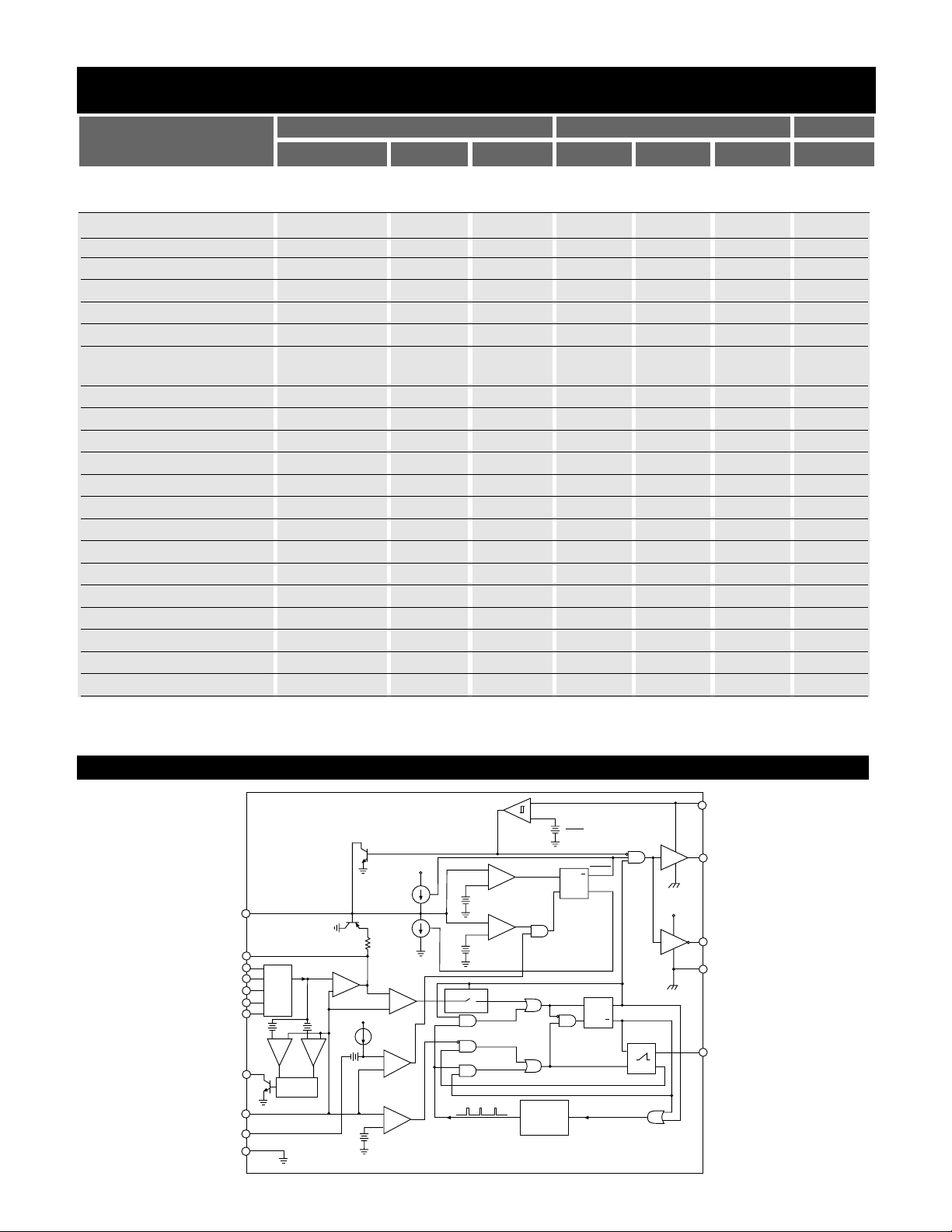
Block Diagram
6
CS5166H
Electrical Characteristics: 0˚C < TA< 70˚C; 0˚C < TJ< 125˚C; 8V < VCC< 20V; 2.0V DAC Code (V
ID4
= V
ID3
= V
ID2
=
V
ID1
=0, V
ID0
= 1), C
GATE(H
) = C
GATE(L)
= 3.3nF, C
OFF
= 330pF, CSS= 0.1µF; Unless otherwise stated.
% of Nominal V
ID
Code -12 -8.5 -5 5 8.5 12 %
■ DAC CODE
V
ID4VID3VID2VID1VID0
1 1 0 1 1 2.134 2.218 2.303 2.546 2.631 2.716 V
1 1 1 0 0 2.046 2.127 2.208 2.441 2.522 2.604 V
1 1 1 0 1 1.958 2.035 2.113 2.336 2.414 2.492 V
1 1 1 1 0 1.870 1.944 2.018 2.231 2.305 2.380 V
0 0 0 0 0 1.826 1.898 1.971 2.178 2.251 2.324 V
0 0 0 0 1 1.782 1.8520 1.923 2.126 2.197 2.268 V
0 0 0 1 0 1.738 1.807 1.876 2.073 2.142 2.212 V
0 0 0 1 1 1.694 1.761 1.828 2.021 2.088 2.156 V
0 0 1 0 0 1.650 1.715 1.781 1.968 2.034 2.100 V
0 0 1 0 1 1.606 1.669 1.733 1.916 1.980 2.044 V
0 0 1 1 0 1.562 1.624 1.686 1.863 1.925 1.988 V
0 0 1 1 1 1.518 1.578 1.638 1.811 1.871 1.932 V
0 1 0 0 0 1.474 1.532 1.591 1.758 1.817 1.876 V
0 1 0 0 1 1.430 1.486 1.543 1.706 1.763 1.820 V
0 1 0 1 0 1.386 1.441 1.496 1.653 1.708 1.764 V
0 1 0 1 1 1.342 1.395 1.448 1.601 1.654 1.708 V
0 1 1 0 0 1.298 1.349 1.401 1.548 1.600 1.652 V
0 1 1 0 1 1.254 1.303 1.353 1.496 1.546 1.596 V
0 1 1 1 0 1.210 1.258 1.306 1.443 1.491 1.540 V
0 1 1 1 1 1.166 1.212 1.258 1.391 1.437 1.484 V
1 1 1 1 1 1.094 1.138 1.181 1.306 1.349 1.393 V
Note 1: Guaranteed by design, not 100% tested in production
5V
60µA
COMP
V
V
V
V
V
PWRGD
V
I
SENSE
LGnd
SS
5 BIT
DAC
+8.5%
-+-
65µS
Delay
ERROR AMPLIFIER
+
-
+
76mV
ID0
ID1
ID2
ID3
ID4
-8.5%
FB
2µA
PWM
COMPARATOR
-
+
V
CC
30µA
-
+
I
SENSE
COMPARATOR
-
+
VFB LOW COMPARATOR
1V
2.5V
VCC Monitor
PWM Comp
Blanking
0.7V
Extended
-
+
+
-
Maximum
On-Time
Timeout
Normal
Off-Time
Off-Time
Timeout
-
+
SS Low
Comparator
SS High
Comparator
Time Out
Timer
3.95V
3.87V
R
S
FAULT
Latch
Off-Time
Timeout
FAULT
Q
FAULT
Q
Q
R
S
Q
PWM
Latch
Edge Triggered
GATE(H) = ON
GATE(H) = OFF
C
OFF
One Shot
R
S
Q
V
CC
V
GATE(H)
PGnd
V
CC
V
GATE(L)
PGnd
C
OFF
CS5166H
7
V
2
TM
Control Method
The V
2
TM
method of control uses a ramp signal that is generated by the ESR of the output capacitors. This ramp is
proportional to the AC current through the main inductor
and is offset by the value of the DC output voltage. This
control scheme inherently compensates for variation in
either line or load conditions, since the ramp signal is generated from the output voltage itself. This control scheme
differs from traditional techniques such as voltage mode,
which generates an artificial ramp, and current mode,
which generates a ramp from inductor current.
Figure 1: V
2
TM
Control Diagram.
The V
2
TM
control method is illustrated in Figure 1. The output voltage is used to generate both the error signal and
the ramp signal. Since the ramp signal is simply the output
voltage, it is affected by any change in the output regardless of the origin of that change. The ramp signal also contains the DC portion of the output voltage, which allows
the control circuit to drive the main switch to 0% or 100%
duty cycle as required.
A change in line voltage changes the current ramp in the
inductor, affecting the ramp signal, which causes the V
2
TM
control scheme to compensate the duty cycle. Since the
change in inductor current modifies the ramp signal, as in
current mode control, the V
2
TM
control scheme has the same
advantages in line transient response.
A change in load current will have an affect on the output
voltage, altering the ramp signal. A load step immediately
changes the state of the comparator output, which controls
the main switch. Load transient response is determined
only by the comparator response time and the transition
speed of the main switch. The reaction time to an output
load step has no relation to the crossover frequency of the
error signal loop, as in traditional control methods.
The error signal loop can have a low crossover frequency,
since transient response is handled by the ramp signal
loop. The main purpose of this ‘slow’ feedback loop is to
provide DC accuracy. Noise immunity is significantly
improved, since the error amplifier bandwidth can be
rolled off at a low frequency. Enhanced noise immunity
improves remote sensing of the output voltage, since the
noise associated with long feedback traces can be effectively filtered.
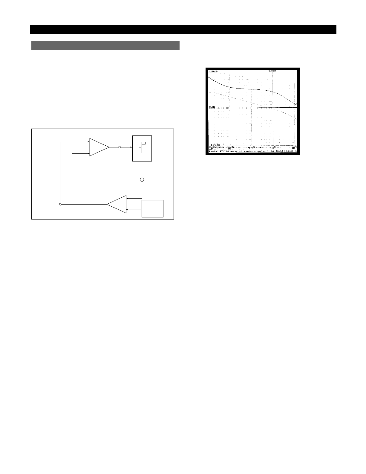
The Bode plot in Figure 2 shows the gain and phase margin
of the CS5166H single pole feedback loop and demonstrates the overall stability of the CS5166H-based regulator.
Figure 2: Feedback loop Bode Plot.
Line and load regulation are drastically improved because
there are two independent voltage loops. A voltage mode
controller relies on a change in the error signal to compensate for a deviation in either line or load voltage. This
change in the error signal causes the output voltage to
change corresponding to the gain of the error amplifier,
which is normally specified as line and load regulation.
A current mode controller maintains fixed error signal
under deviation in the line voltage, since the slope of the
ramp signal changes, but still relies on a change in the error
signal for a deviation in load. The V
2
TM
method of control
maintains a fixed error signal for both line and load variation, since the ramp signal is affected by both line and load.
Constant Off-Time
To maximize transient response, the CS5166H uses a
Constant Off-Time method to control the rate of output
pulses. During normal operation, the Off-Time of the high
side switch is terminated after a fixed period, set by the
C
OFF
capacitor. To maintain regulation, the V
2
TM
Control
Loop varies switch On-Time. The PWM comparator monitors the output voltage ramp, and terminates the switch
On-Time.
Constant Off-Time provides a number of advantages.
Switch duty Cycle can be adjusted from 0 to 100% on a
pulse-by pulse basis when responding to transient conditions. Both 0% and 100% Duty Cycle operation can be
maintained for extended periods of time in response to
Load or Line transients. PWM Slope Compensation to
avoid sub-harmonic oscillations at high duty cycles is
avoided.
Switch On-Time is limited by an internal 30µs (typical)
timer, minimizing stress to the Power Components
Programmable Output
The CS-5166H is designed to provide two methods for programming the output voltage of the power supply. A five
bit on board digital to analog converter (DAC) is used to
program the output voltage within two different ranges.
Theory Of Operation
Application Information
COMP
PWM
Comparator
+
C
–
Ramp Signal
Error
Signal
Error
Amplifier
GATE(H)
GATE(L)
E
V
FB
–
+
Reference
Voltage
.1µF
10K
Open Loop
49.63
BW
62.3 KHz
Phase margin
81.9
 Loading...