

Cherry Semiconductor CS5165H Datasheet
Features
■ V
2
™
Control Topology
■ Dual N Channel Design
■ 100ns Controller Transient
Response
■ Excess of 1Mhz Operation
■ 5 Bit DAC with 1% Tolerance
■ Power Good Output With
Internal Delay
■ Enable Input Provides
Micropower Shutdown Mode
■ Complete Pentium
®
II System
Requires 18 Components
■ 5V and 12V Operation Using
Either Dual or Single Supplies
■ Adaptive Voltage Positioning
■ Remote Sense Capability
■ Current Sharing Capability
■ V
CC
Monitor
■ Hiccup Mode Short Circuit
Protection
■ Overvoltage Protection (OVP)
■ Programmable Soft Start
■ 150ns PWM Blanking
■ 65ns FET Non-Overlap
■ 40ns Gate Rise and Fall Times
(3.3nF load)
Package Options
CS5165H
Fast, Precise 5-Bit Synchronous Buck Controller
for the Next Generation Low Voltage Pentium® II Processors
CS5165H
Description
The CS5165H synchronous 5-bit NFET
buck controller is optimized to manage
the power of the next generation
Pentium
®
II processors. It’s V
2
™
control
architecture delivers the fastest transient
response (100ns), and best overall voltage
regulation in the industry today. It’s feature rich design gives end users the maximum flexibility to implement the best
price/performance solutions for their end
products.
The CS5165H has been carefully crafted
to maximize performance and protect the
processor during operation. It has a 5-bit
DAC on board that holds a ±1% tolerance
over temperature. Its on board programmable soft start insures a control
start up, and the FET nonoverlap circuitry ensures that both FETs do not conduct
simultaneously.
The on board oscillator can be programmed up to 1MHz to give the designer maximum flexibility in choosing external components and setting systems
costs.
The CS5165H protects the processor during potentially catastrophic events like
overvoltage (OVP) and short circuit. The
OVP feature is part of the V
2
™
architecture and does not require any additional
components. During short circuit, the
controller pulses the MOSFETs in a “hiccup” mode (3% duty cycle) until the fault
is removed. With this method, the
MOSFETs do not overheat or self
destruct.
The CS5165H is designed for use in both
single processor desktop and multiprocessor workstation and server applications. The IC can be powered from either
single or dual 5V, 12V power supplies.
The CS5165H’s current sharing capability
allows the designer to build multiple parallel and redundant power solutions for
multiprocessor systems.
The CS5165H contains other control and
protection features such as Power Good,
ENABLE, and adaptive voltage positioning. It is available in a 16 lead SOIC wide
body package.
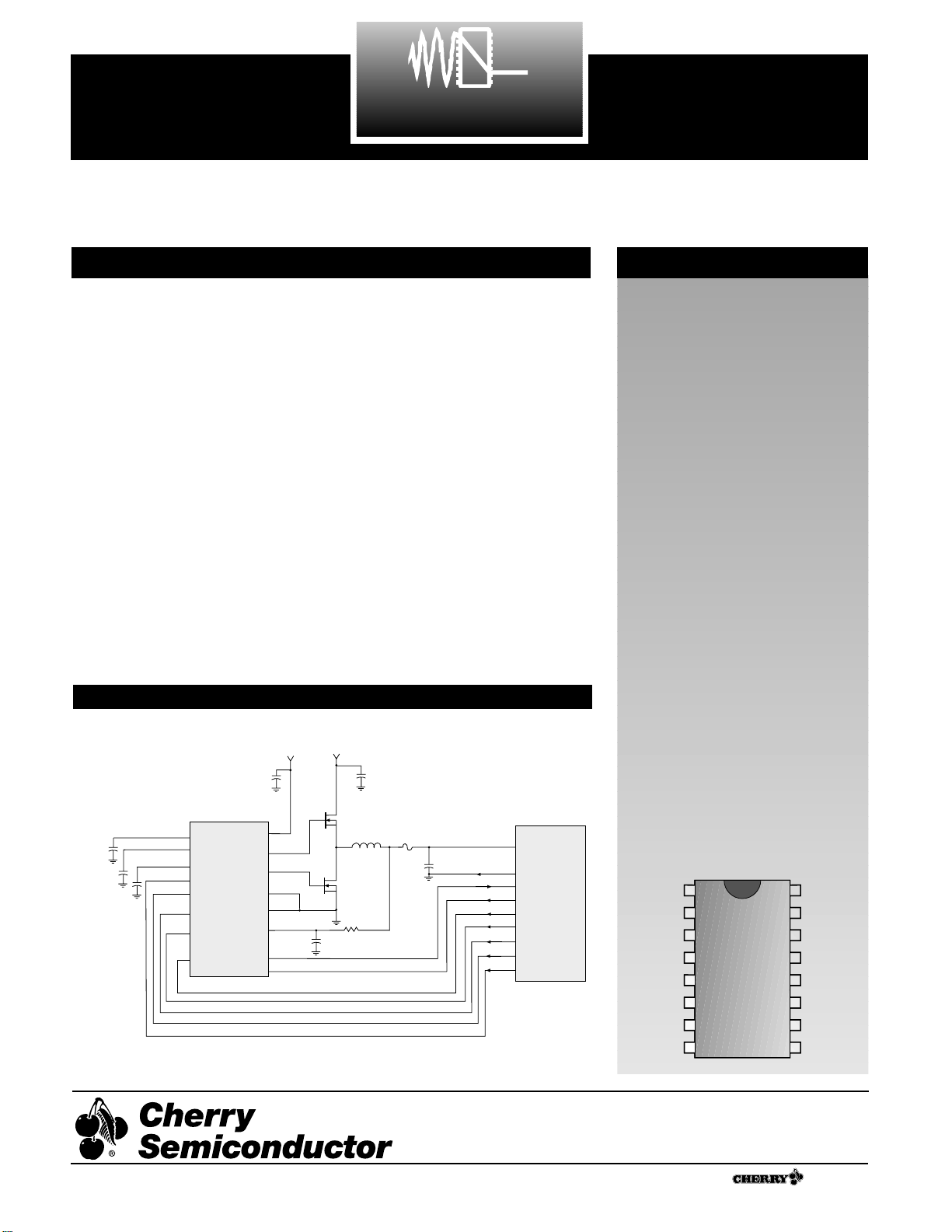
Application Diagram
16 Lead SO WIDE
1
V
ID0
V
ID1
V
ID2
V
ID3
ENABLE
C
OFF
SS
V
ID4
V
FB
COMP
LGnd
PWRGD
GATE(L)
PGnd
GATE(H)
V
CC
V2is a trademark of Switch Power, Inc.
Pentium is a registered trademark of Intel Corporation.
5V to 2.8V @ 14.2A for 300MHz Pentium
®
II
Rev. 12/24/98
Cherry Semiconductor Corporation
2000 South County Trail, East Greenwich, RI 02818
Tel: (401)885-3600 Fax: (401)885-5786
Email: info@cherry-semi.com
Web Site: www.cherry-semi.com
A Company
®
12V
1µF
V
SS
0.1µF
0.1 µF
330pF
COMP
C
OFF
V
V
V
V
V
ID4
ID3
ID2
ID1
ID0
CS5165H
CC
GATE(H)
GATE(L)
PGnd
LGnd
V
FB
PWRGD
ENABLE
5V
1200µF/10V x 3
IRL3103
IRL3103
3.3K
1000pF
1.2µH
PCB
trace 6mΩ
1200µF
10V x 5
V
V
PWRGD
ENABLE
V
ID0
V
ID1
V
ID2
V
ID3
V
ID4
CC
SS
Pentium® II
System
1
Absolute Maximum Ratings
Pin Symbol Pin Name
V
MAX
V
MIN
I
SOURCE
I
SINK
2
PACKAGE PIN # PIN SYMBOL FUNCTION
Package Pin Description
CS5165H
1,2,3,4,6 V
ID0-VID4
Voltage ID DAC inputs. These pins are internally pulled up to 5V if left open.
V
ID4
selects the DAC range. When V
ID4
is high (logic one), the Error Amp ref-
erence range is 2.14V to 3.54V with 100mV increments. When V
ID4
is low (logic
zero), the Error amp reference voltage is 1.34V to 2.09V with 50mV increments.
5 SS Soft Start Pin. A capacitor from this pin to LGnd sets the Soft Start and fault
timing.
7 C
OFF
Off-Time Capacitor Pin. A capacitor from this pin to LGnd sets both the normal and extended off time.
8 ENABLE Output Enable Input. This pin is internally pulled up to 1.8V. A logic Low
( < 0.8V) on this pin disables operation and places the CS5165H into a low
current sleep mode.
9 V
CC
Input Power Supply Pin.
10 GATE(H) High Side Switch FET driver pin.
11 PGnd High Current ground for the GATE(H) and GATE(L) pins.
12 GATE(L) Low Side Synchronous FET driver pin.
13 PWRGD Power Good Output. Open collector output drives low when VFBis out of
regulation. Active when ENABLE input is low
14 LGnd Reference ground. All control circuits are referenced to this pin.
15 COMP Error Amp output. PWM Comparator reference input. A capacitor to LGnd
provides Error Amp compensation.
16 V
FB
Error Amp, PWM Comparator, and Low VFBComparator feedback input.
V
CC
IC Power Input 20V -0.3V N/A 1.5A Peak
200mA DC
SS Soft Start Capacitor 6V -0.3V 200µA 10µA
COMP Compensation Capacitor 6V -0.3V 10mA 1mA
V
FB
Voltage Feedback Input 6V -0.3V 10µA 10µA
C
OFF
Off-Time Capacitor 6V -0.3V 1mA 50mA
V
ID0-4
Voltage ID DAC Inputs 6V -0.3V 1mA 10µA
GATE(H) High-Side FET Driver 20V -0.3V 1.5A Peak; 1.5A Peak;
200mA DC 200mA DC
GATE(L) Low-Side FET Driver 20V -0.3V 1.5A Peak; 1.5A Peak;
200mA DC 200mA DC
ENABLE Enable Input 6V -0.3V 100µA 1mA
PWRGD Power-Good Output 6V -0.3V 10µA 30mA
PGnd Power Ground 0V 0V 1.5A Peak N/A
200mA DC
LGnd Logic Ground 0V 0V 100mA N/A
Operating Junction Temperature, TJ . . . . . . . . . . . . . . . . . . . . . . . . . . . . . . . . . . . . . . . . . . . . . . . . . . . . . . . . . . . . . 0 to 150°C
Lead Temperature Soldering:
Reflow (SMD styles only) . . . . . . . . . . . . . . . . . . . . . . . . . . . . . . . . . . . . . . . . . . .60 Sec max. above 183°C, 230°C Peak
Storage Temperature Range, T
S
. . . . . . . . . . . . . . . . . . . . . . . . . . . . . . . . . . . . . . . . . . . . . . . . . . . . . . . . . . . . . −65°C to 150°C
ESD Susceptibility . . . . . . . . . . . . . . . . . . . . . . . . . . . . . . . . . . . . . . . . . . . . . . . . . . . . . . . . . . . . . . . . . . . . . . . . . . . . . . . . . . 2kV

■ V
CC
Supply Current
Operating 1V < VFB< V
DAC
(max on-time) 12 20 mA
No Loads on Gate(H) and Gate(L)
Sleep Mode ENABLE = 0V, 8V< V
CC
<14V 300 600 µA
■ V
CC
Monitor
Start Threshold GATE(H) Switching 3.75 3.95 4.15 V
Stop Threshold GATE(H) not switching 3.65 3.87 4.05 V
Hysteresis Start - Stop 80 mV
■ Error Amplifier
V
FB
Bias Current VFB= 0V 0.1 1.0 µA
COMP Source Current COMP = 1.2V to 3.6V; VFB= 2.7V 15 30 60 µA
COMP CLAMP Voltage VFB= 2.7V, Adjust COMP voltage for 0.85 1.0 1.15 V
Comp current = 50µA
COMP Clamp Current COMP = 0V 0.4 1.0 1.6 mA
COMP Sink Current V
COMP
=1.2V; V
FB
= 3V; VSS> 2.5V 180 400 800 µA
Open Loop Gain Note 1 50 60 dB
Unity Gain Bandwidth Note 1 0.5 2 MHz
PSRR @ 1kHZ Note 1 60 85 dB
■ GATE(H) and GATE(L)
High Voltage at 100mA Measure V
CC
-GATE 1.2 2.0 V
Low Voltage at 100mA Measure GATE 1.0 1.5 V
Rise Time 1.6V < GATE < (V
CC
- 2.5V),
8V < V
CC
< 14V 40 80 ns
Fall Time (V
CC
- 2.5V) > GATE > 1.6V,
8V < V
CC
< 14V 40 80 ns
GATE(H) to GATE(L) Delay GATE(H) < 2V, GATE(L) > 2V,
8V < V
CC
< 14V 30 65 100 ns
GATE(L) to GATE(H) Delay GATE(L) < 2V, GATE(H) > 2V,
8V < V
CC
< 14V 30 65 100 ns
GATE pull-down Resistance to PGnd (note 1) 20 50 115 kΩ
■ Fault Protection
SS Charge Time VFB= 0V 1.6 3.3 5.0 ms
SS Pulse Period VFB= 0V 25 100 200 ms
SS Duty Cycle (Charge Time/Period) × 100 1.0 3.3 6.0 %
SS Comp Clamp Voltage V
FB
= 2.7V, VSS= 0V 0.50 0.95 1.10 V
VFBLow Comparator Increase VFBtill no SS 0.9 1.0 1.1 V
pulsing and normal Off-time.
■ PWM Comparator
Transient Response VFB= 1.2 to 5V 500ns after 100 150 ns
GATE(H) (after Blanking time) to
GATE(H) = (VCC- 1V) to 1V,
8V < V
CC
< 14V
CS5165H
3
Electrical Characteristics: 0˚C < TA< 70˚C; 0˚C < TJ < 125˚C; 8V < VCC< 20V; 2.8V DAC Code (V
ID4=VID2=VID1=VID0
=1, V
ID3
= 0),
C
GATE(H)
= C
GATE(L)
= 3.3nF, C
OFF
= 330pF, CSS= 0.1µF; Unless otherwise stated.
PARAMETER TEST CONDITIONS MIN TYP MAX UNIT
CS5165H
4
Electrical Characteristics: 0˚C < TA< 70˚C; 0˚C < TJ < 125˚C; 8V < VCC< 20V; 2.8V DAC Code (V
ID4=VID2=VID1=VID0
=1, V
ID3
= 0),
C
GATE(H)
= C
GATE(L)
= 3.3nF, C
OFF
= 330pF, CSS= 0.1µF; Unless otherwise stated.
■ Voltage Identification DAC
Accuracy (all codes except 11111) Measure V
FB
= COMP (C
OFF
= 0V) -1 +1 %
V
ID4VID3VID2VID1VID0
25˚C ≤ TJ≤ 125˚C; VCC= 12V
1 0 0 0 0 3.505 3.540 3.575 V
1 0 0 0 1 3.406 3.440 3.474 V
1 0 0 1 0 3.307 3.340 3.373 V
1 0 0 1 1 3.208 3.240 3.272 V
1 0 1 0 0 3.109 3.140 3.171 V
1 0 1 0 1 3.010 3.040 3.070 V
1 0 1 1 0 2.911 2.940 2.969 V
1 0 1 1 1 2.812 2.840 2.868 V
1 1 0 0 0 2.713 2.740 2.767 V
1 1 0 0 1 2.614 2.640 2.666 V
1 1 0 1 0 2.515 2.540 2.565 V
1 1 0 1 1 2.416 2.440 2.464 V
1 1 1 0 0 2.317 2.340 2.363 V
1 1 1 0 1 2.218 2.240 2.262 V
1 1 1 1 0 2.119 2.140 2.161 V
0 0 0 0 0 2.069 2.090 2.111 V
0 0 0 0 1 2.020 2.040 2.060 V
0 0 0 1 0 1.970 1.990 2.010 V
0 0 0 1 1 1.921 1.940 1.959 V
0 0 1 0 0 1.871 1.890 1.909 V
0 0 1 0 1 1.822 1.840 1.858 V
0 0 1 1 0 1.772 1.790 1.808 V
0 0 1 1 1 1.723 1.740 1.757 V
0 1 0 0 0 1.673 1.690 1.707 V
0 1 0 0 1 1.624 1.640 1.656 V
PARAMETER TEST CONDITIONS MIN TYP MAX UNIT
■ PWM Comparator: continued
Minimum Pulse Width Drive VFB1.2 to 5V upon 50 150 250 ns
(Blanking Time) GATE(H) rising edge (> VCC-1V),
measure GATE(H ) pulse width,
8V < V
CC
< 14V
■ C
OFF
Normal Off-Time VFB= 2.7V 1.0 1.6 2.3 µs
Extended Off-Time VSS= VFB= 0V 5.0 8.0 12.0 µs
■ Time-Out Timer
Time-Out Time VFB= 2.7V, Measure
GATE(H ) Pulse Width 10 30 50 µs
Fault Duty Cycle VFB= 0V 30 50 70 %
■ Enable Input
ENABLE Threshold GATE(H) Switching 0.8 1.15 1.30 V
Shutdown delay (Note 1) ENABLE-to-GATE(H) < 2V 3 µs
Pull-up Current ENABLE = 0V 3 7 15 µA
Pull-up Voltage No load on ENABLE pin 1.30 1.8 3 V
Input Resistance ENABLE = 5V,
R = (5V-V
PULLUP
)/I
ENABLE
10 20 50 kΩ
CS5165H
5
PARAMETER TEST CONDITIONS MIN TYP MAX UNIT
THRESHOLD ACCURACY
LOWER THRESHOLD UPPER THRESHOLD
MIN TYP MAX MIN TYP MAX UNIT
% of Nominal DAC Output -12 -8.5 -5 5 8.5 12 %
■ DAC CODE
V
ID4VID3VID2VID1VID0
1 0 0 0 0 3.115 3.239 3.363 3.717 3.841 3.965 V
1 0 0 0 1 3.027 3.148 3.268 3.612 3.732 3.853 V
1 0 0 1 0 2.939 3.056 3.173 3.507 3.624 3.741 V
1 0 0 1 1 2.851 2.965 3.078 3.402 3.515 3.629 V
1 0 1 0 0 2.763 2.873 2.983 3.297 3.407 3.517 V
1 0 1 0 1 2.675 2.782 2.888 3.192 3.298 3.405 V
1 0 1 1 0 2.587 2.690 2.793 3.087 3.190 3.293 V
1 0 1 1 1 2.499 2.599 2.698 2.982 3.081 3.181 V
1 1 0 0 0 2.411 2.507 2.603 2.877 2.973 3.069 V
1 1 0 0 1 2.323 2.416 2.508 2.772 2.864 2.957 V
1 1 0 1 0 2.235 2.324 2.413 2.667 2.756 2.845 V
1 1 0 1 1 2.147 2.233 2.318 2.562 2.647 2.733 V
1 1 1 0 0 2.059 2.141 2.223 2.457 2.539 2.621 V
1 1 1 0 1 1.971 2.050 2.128 2.352 2.430 2.509 V
1 1 1 1 0 1.883 1.958 2.033 2.250 2.322 2.397 V
0 0 0 0 0 1.839 1.912 1.986 2.195 2.268 2.341 V
0 0 0 0 1 1.795 1.867 1.938 2.142 2.213 2.285 V
0 0 0 1 0 1.751 1.821 1.810 2.090 2.159 2.229 V
0 0 0 1 1 1.707 1.775 1.843 2.037 2.105 2.173 V
0 0 1 0 0 1.663 1.729 1.796 1.985 2.051 2.117 V
0 0 1 0 1 1.619 1.684 1.748 1.932 1.996 2.061 V
0 0 1 1 0 1.575 1.638 1.701 1.880 1.942 2.005 V
0 0 1 1 1 1.531 1.592 1.653 1.827 1.888 1.949 V
V
ID4VID3VID2VID1VID0
0 1 0 1 0 1.574 1.590 1.606 V
0 1 0 1 1 1.525 1.540 1.555 V
0 1 1 0 0 1.475 1.490 1.505 V
0 1 1 0 1 1.426 1.440 1.455 V
0 1 1 1 0 1.376 1.390 1.405 V
0 1 1 1 1 1.327 1.340 1.353 V
1 1 1 1 1 1.223 1.247 1.273 V
Input Threshold V
ID4
, V
ID3
, V
ID2
, V
ID1
, V
ID0
1.000 1.250 2.400 V
Input Pull-up Resistance V
ID4
, V
ID3
, V
ID2
, V
ID1
, V
ID0
25 50 100 kΩ
Input Pull-up Voltage 4.85 5.00 5.15 V
■ Power Good Output
Low to High Delay V
FB
= (0.8 × V
DAC
) to V
DAC
30 65 110 µs
High to Low Delay V
FB
= V
DAC
to (0.8 × V
DAC
) 30 75 120 µs
Output Low Voltage V
FB
= 2.4V, I
PWRGD
= 500µA 0.2 0.3 V
Sink Current Limit V
FB
= 2.4V, PWRGD = 1V 0.5 4.0 15.0 mA
Electrical Characteristics: 0˚C < TA< 70˚C; 0˚C < TJ < 125˚C; 8V < VCC< 20V; 2.8V DAC Code (V
ID4=VID2=VID1=VID0
=1, V
ID3
= 0),
C
GATE(H)
= C
GATE(L)
= 3.3nF, C
OFF
= 330pF, CSS= 0.1µF; Unless otherwise stated.
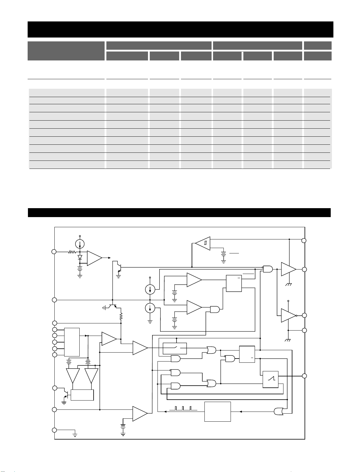
Block Diagram
6
CS5165H
THRESHOLD ACCURACY
LOWER THRESHOLD UPPER THRESHOLD
MIN TYP MAX MIN TYP MAX UNITS
% of Nominal DAC Output -12 -8.5 -5 5 8.5 12 %
■ DAC CODE
V
ID4VID3VID2VID1VID0
0 1 0 0 0 1.487 1.546 1.606 1.775 1.834 1.893 V
0 1 0 0 1 1.443 1.501 1.558 1.722 1.779 1.837 V
0 1 0 1 0 1.399 1.455 1.511 1.670 1.725 1.781 V
0 1 0 1 1 1.355 1.409 1.463 1.617 1.671 1.724 V
0 1 1 0 0 1.311 1.363 1.416 1.565 1.617 1.669 V
0 1 1 0 1 1.267 1.318 1.368 1.512 1.562 1.613 V
0 1 1 1 0 1.223 1.272 1.321 1.460 1.508 1.557 V
0 1 1 1 1 1.179 1.226 1.273 1.407 1.454 1.501 V
1 1 1 1 1 1.097 1.141 1.185 1.309 1.353 1.397 V
Note 1: Guaranteed by design, not 100% tested in production.
Electrical Characteristics: 0˚C < TA< 70˚C; 0˚C < TJ < 125˚C; 8V < VCC< 20V; 2.8V DAC Code (V
ID4=VID2=VID1=VID0
=1, V
ID3
= 0),
C
GATE(H)
= C
GATE(L)
= 3.3nF, C
OFF
= 330pF, CSS= 0.1µF; Unless otherwise stated.
5V
VFB Low
Comparator
Monitor
V
CC
2.5V
PWM Comp
Blanking
0.7V
Normal
Off-Time
Extended
Off-Time
Timeout
-
+
SS High
Comparator
+
-
Maximum
On-Time
Timeout
+
SS Low
Comparator
Time Out
Timer
(30µs)
3.95V
3.87V
R
S
FAULT
Latch
Off-Time
Timeout
FAULT
Q
FAULT
Q
Q
R
S
Q
PWM
Latch
Edge Triggered
V
GATE(H) = ON
GATE(H) = OFF
C
OFF
One Shot
R
S
Q
PGnd
CC
ENABLE
SS
COMP
V
V
V
V
V
PWRGD
V
FB
LGnd
ID0
ID1
ID2
ID3
ID4
-8.5%
20k
1.25V
5 BIT
DAC
V
CC
+8.5%
-+-
65µs
Delay
7µA
-
+
Enable
Comparator
Error Amplifier
+
-
+
Circuit Bias
1V
60µA
2µA
-
+
PWM
Comparator
-
+
V
CC
V
GATE(H)
V
GATE(L)
PGnd
C
OFF
 Loading...