

Cherry Semiconductor CS5150GN16, CS5150GDR16, CS5150GD16 Datasheet
The CS5150 is a 4-bit synchronous
dual N-Channel buck controller. It
is designed to provide unprecedented transient response for
today’s demanding high-density,
high-speed logic. The regulator
operates using a proprietary control
method, which allows a 100ns
response time to load transients.
The CS5150 is designed to operate
over a 4.25-16V range (VCC) using
12V to power the IC and 5V as the
main supply for conversion.
The CS5150 is specifically designed
to power Pentium®Pro processors
and other high performance core
logic. It includes the following features: on board, 4-bit DAC, short
circuit protection, 1.0% output tolerance, VCCmonitor, and programmable soft start capability. The
CS5150 is upward compatible with
the 5-bit CS5155, allowing the
mother board designer the capability of using either the CS5150 or the
CS5155 with no change in layout.
The CS5150 is available in 16 pin
surface mount and DIP packages.
Features
■ Dual N-Channel Design
■ Excess of 1MHz Operation
■ 100ns Transient Response
■ 4-Bit DAC
■ Upward Compatible with
5-Bit CS5155/5156 and
Adjustable CS5120/5121
■ 30ns Gate Rise/Fall Times
■ 1% DAC Accuracy
■ 5V & 12V Operation
■ Remote Sense
■ Programmable Soft Start
■ Lossless Short Circuit
Protection
■ V
CC
Monitor
■ 25ns FET Nonoverlap Time
■ Adaptive Voltage
Positioning
■ V
2
™
Control Topology
■ Current Sharing
■ Overvoltage Protection
Package Options
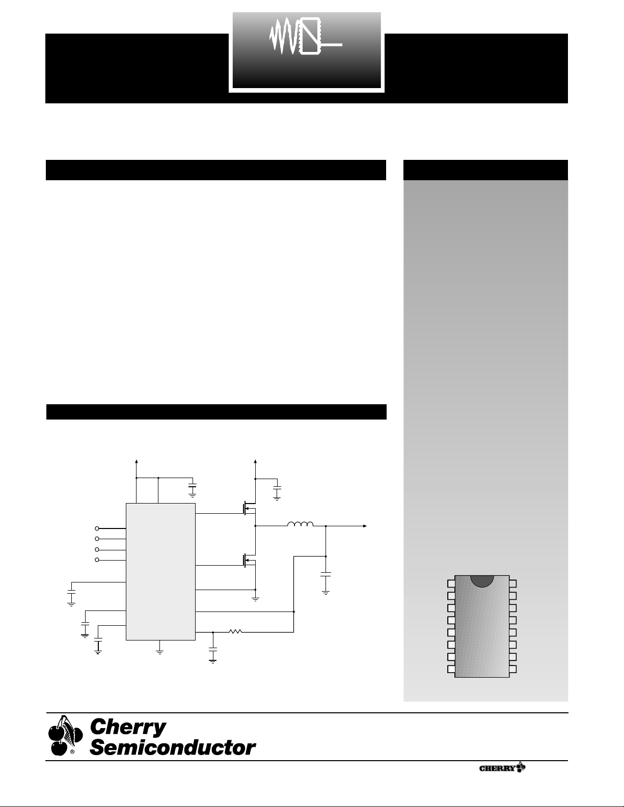
CPU 4-Bit Synchronous Buck Controller
CS5150
Description
Application Diagram
V
ID0
V
ID1
V
ID2
V
ID3
SS
NC
C
OFF
V
FFB
V
FB
COMP
LGnd
V
CC1
V
GATE(L)
PGnd
V
GATE(H)
V
CC2
16 Lead SO Narrow & PDIP
1
Switching Power Supply for core logic - Pentium®Pro processor
0.33µF
V
ID0
V
ID1
V
ID2
V
ID3
V
ID0
V
ID1
V
ID2
V
ID3
V
CC1
SS
CS5150
C
OFF
LGnd
V
FB
V
FFB
COMP
IRL3103
IRL3103
0.1µF
12V 5V
2µH
2.1V to 3.5V @ 13A
V
CC2
V
GATE(H)
V
GATE(L)
PGnd
1200µF/16V x 3
AlEl
3.3k
0.1µF
1200µF/16V x 5
AlEl
100pF
330pF
V2is a trademark of Switch Power, Inc.
Pentium is a registered trademark of Intel Corporation.
Rev. 1/4/99
Cherry Semiconductor Corporation
2000 South County Trail, East Greenwich, RI 02818
Tel: (401)885-3600 Fax: (401)885-5786
Email: info@cherry-semi.com
Web Site: www.cherry-semi.com
A Company
®
CS5150
1
2
Pin Name Max Operating Voltage Max Current
V
CC1
. . . . . . . . . . . . . . . . . . . . . . . . . . . . . . . . . . . .16V/-0.3V . . . . . . . . . . . . . . . . . . . . . . . . . . . . . . .25mA DC/1.5A peak
V
CC2
. . . . . . . . . . . . . . . . . . . . . . . . . . . . . . . . . . . .16V/-0.3V . . . . . . . . . . . . . . . . . . . . . . . . . . . . . . .20mA DC/1.5A peak
SS . . . . . . . . . . . . . . . . . . . . . . . . . . . . . . . . . . . . . .6V/-0.3V . . . . . . . . . . . . . . . . . . . . . . . . . . . . . . . . . . . . . . . . . . . . .-100µA
COMP . . . . . . . . . . . . . . . . . . . . . . . . . . . . . . . . . .6V/-0.3V . . . . . . . . . . . . . . . . . . . . . . . . . . . . . . . . . . . . . . . . . . . . .200µA
VFB . . . . . . . . . . . . . . . . . . . . . . . . . . . . . . . . . . . . .6V/-0.3V . . . . . . . . . . . . . . . . . . . . . . . . . . . . . . . . . . . . . . . . . . . . .-0.2µA
C
OFF
. . . . . . . . . . . . . . . . . . . . . . . . . . . . . . . . . . . .6V/-0.3V . . . . . . . . . . . . . . . . . . . . . . . . . . . . . . . . . . . . . . . . . . . . .-0.2µA
V
FFB
. . . . . . . . . . . . . . . . . . . . . . . . . . . . . . . . . . . .6V/-0.3V . . . . . . . . . . . . . . . . . . . . . . . . . . . . . . . . . . . . . . . . . . . . .-0.2µA
V
ID0
- V
ID3
. . . . . . . . . . . . . . . . . . . . . . . . . . . . . . .6V/-0.3V . . . . . . . . . . . . . . . . . . . . . . . . . . . . . . . . . . . . . . . . . . . . . .-50µA
V
GATE(H)
. . . . . . . . . . . . . . . . . . . . . . . . . . . . . . . .16V/-0.3V . . . . . . . . . . . . . . . . . . . . . . . . . . . . . .100mA DC/1.5A peak
V
GATE(L)
. . . . . . . . . . . . . . . . . . . . . . . . . . . . . . . . .16V/-0.3V . . . . . . . . . . . . . . . . . . . . . . . . . . . . . .100mA DC/1.5A peak
LGnd . . . . . . . . . . . . . . . . . . . . . . . . . . . . . . . . . . .0V . . . . . . . . . . . . . . . . . . . . . . . . . . . . . . . . . . . . . . . . . . . . . . . . . . . .25mA
PGnd . . . . . . . . . . . . . . . . . . . . . . . . . . . . . . . . . . .0V . . . . . . . . . . . . . . . . . . . . . . . . . . . . . . . . . . . . .100mA DC/1.5A peak
Operating Junction Temperature, TJ . . . . . . . . . . . . . . . . . . . . . . . . . . . . . . . . . . . . . . . . . . . . . . . . . . . . . . . . . . .°0 to 150°C
Lead Temperature Soldering
Wave Solder (through hole styles only) . . . . . . . . . . . . . . . . . . . . . . . . . . . . . . . . . . . . . . . . . . .10 sec. max, 260°C peak
Reflow (SMD styles only) . . . . . . . . . . . . . . . . . . . . . . . . . . . . . . . . . . . . . . . . . . .60 sec. max above 183°C, 230°C peak
Storage Temperature Range, TS . . . . . . . . . . . . . . . . . . . . . . . . . . . . . . . . . . . . . . . . . . . . . . . . . . . . . . . . . . . . .-65° to 150°C
ESD Susceptibility . . . . . . . . . . . . . . . . . . . . . . . . . . . . . . . . . . . . . . . . . . . . . . . . . . . . . . . . . . . . . . . . . . . . . . . . . . . . . . . .2kV
PARAMETER TEST CONDITIONS MIN TYP MAX UNIT
CS5150
Electrical Characteristics:
0°C < TA< +70°C; 0°C < TJ< +85°C; 8V < V
CC1
< 14V; 5V < V
CC2
< 14V; DAC Code: V
ID2
= V
ID1
=
V
ID0
= 1; V
ID3
= 0; CV
GATE(L)
and CV
GATE(H)
= 1nF; C
OFF
= 330pF; CSS= 0.1µF, unless otherwise specified.
Absolute Maximum Ratings
■ Error Amplifier
VFBBias Current VFB= 0V 0.3 1.0 µA
Open Loop Gain 1.25V < V
COMP
< 4V; Note 1 50 60 dB
Unity Gain Bandwidth Note 1 500 3000 kH
COMP SINK Current V
COMP
= 1.5V; VFB= 3V; VSS> 2V 0.4 2.5 8.0 mA
COMP SOURCE Current V
COMP
= 1.2V; VFB= 2.7V; VSS= 5V 30 50 70 µA
COMP CLAMP Current V
COMP
= 0V; VFB= 2.7V 0.4 1.0 1.6 mA
COMP High Voltage VFB= 2.7V; VSS= 5V 4.0 4.3 5.0 V
COMP Low Voltage VFB=3V 160 600 mV
PSRR 8V < V
CC1
< 14V @ 1kHz; Note 1 60 85 dB
■ V
CC1
Monitor
Start Threshold Output switching 3.75 3.90 4.05 V
Stop Threshold Output not switching 3.70 3.85 4.00 V
Hysteresis Start-Stop 50 mV
■ DAC
Input Threshold V
ID0
, V
ID1
, V
ID2
, V
ID3
1.00 1.25 2.40 V
Input Pull Up Resistance V
ID0
, V
ID1
, V
ID2
, V
ID3
25 50 100 kΩ
Pull Up Voltage 4.85 5.00 5.15 V
Accuracy Measure VFB= V
COMP
, 25°C ≤ TJ≤ 85°C 1.0 %
V
ID3
V
ID2
V
ID1
V
ID0
1 1 1 1 1.2315 1.2440 1.2564 V
1 1 1 0 2.1186 2.1400 2.1614 V
1 1 0 1 2.2176 2.2400 2.2624 V
1 1 0 0 2.3166 2.3400 2.3634 V
1 0 1 1 2.4156 2.4400 2.4644 V
1 0 1 0 2.5146 2.5400 2.5654 V
1 0 0 1 2.6136 2.6400 2.6664 V
1 0 0 0 2.7126 2.7400 2.7674 V
0 1 1 1 2.8116 2.8400 2.8684 V
0 1 1 0 2.9106 2.9400 2.9694 V
CS5150
3
PARAMETER TEST CONDITIONS MIN TYP MAX UNIT
Electrical Characteristics:
0°C < TA< +70°C; 0°C < TJ< +85°C; 8V < V
CC1
< 14V; 5V < V
CC2
< 14V; DAC Code: V
ID2
= V
ID1
=
V
ID0
= 1; V
ID3
= 0; CV
GATE(L)
and CV
GATE(H)
= 1nF; C
OFF
= 330pF; CSS= 0.1µF, unless otherwise specified.
■ DAC: continued
V
ID3
V
ID2
V
ID1
V
ID0
0 1 0 1 3.0096 3.0400 3.0704 V
0 1 0 0 3.1086 3.1400 3.1714 V
0 0 1 1 3.2076 3.2400 3.2724 V
0 0 1 0 3.3066 3.3400 3.3734 V
0 0 0 1 3.4056 3.4400 3.4744 V
0 0 0 0 3.5046 3.5400 3.5754 V
■ V
GATE(H)
and V
GATE(L)
Out SOURCE Sat at 100mA Measure V
CC1
– V
GATE(L),;VCC2
– V
GATE(H)
1.2 2.0 V
Out SINK Sat at 100mA Measure V
GATE(H)
– VPGnd; 1.0 1.5 V
V
GATE(L)
– VPGnd
Out Rise Time 1V < V
GATE(H)
< 9V; 1V < V
GATE(L)
< 9V 30 50 ns
V
CC1
= V
CC2
= 12V
Out Fall Time 9V > V
GATE(H)
> 1V; 9V > V
GATE(L)
> 1V 30 50 ns
V
CC1
= V
CC2
= 12V
Shoot-Through Current Note 1 50 mA
Delay V
GATE(H)
to V
GATE(L)
V
GATE(H)
falling to 2V; V
CC1
= V
CC2
= 8V 25 50 ns
V
GATE(L)
rising to 2V
Delay V
GATE(L)
to V
GATE(H)
V
GATE(L)
falling to 2V; V
CC1
= V
CC2
= 8V 25 50 ns
V
GATE(H)
rising to 2V
V
GATE(H)
, V
GATE(L)
Resistance Resistor to LGnd 20 50 100 kΩ
V
GATE(H)
, V
GATE(L)
Schottky LGnd to V
GATE(H)
@ 10mA 600 800 mV
LGnd to V
GATE(L)
@ 10mA
■ Soft Start (SS)
Charge Time 1.6 3.3 5.0 ms
Pulse Period 25 100 200 ms
Duty Cycle (Charge Time/Pulse Period) × 100 1.0 3.3 6.0 %
COMP Clamp Voltage VFB= 0V; VSS= 0 0.50 0.95 1.10 V
V
FFB
SS Fault Disable V
GATE(H)
= Low; V
GATE(L)
= Low 0.9 1.0 1.1 V
High Threshold 2.5 3.0 V
■ PWM Comparator
Transient Response V
FFB
= 0 to 5V to V
GATE(H)
= 9V to 1V; 100 125 ns
V
CC1
= V
CC2
= 12V
V
FFB
Bias Current V
FFB
= 0V 0.3 µA
■ Supply Current
I
CC1
No Switching 8.5 13.5 mA
I
CC2
No Switching 1.6 3.0 mA
Operating I
CC1
VFB= COMP = V
FFB
813mA
Operating I
CC2
VFB= COMP = V
FFB
25 mA
■ C
OFF
Normal Charge Time V
FFB
= 1.5V; VSS= 5V 1.0 1.6 2.2 µs
Extension Charge Time VSS= V
FFB
= 0 5.0 8.0 11.0 µs
Discharge Current C
OFF
to 5V; V
FB
>1V 5.0 mA

PARAMETER TEST CONDITIONS MIN TYP MAX UNIT
4
CS5150
Package Pin Description
PACKAGE PIN # PIN SYMBOL FUNCTION
Electrical Characteristics:
0°C < TA< +70°C; 0°C < TJ< +85°C; 8V < V
CC1
< 14V; 5V < V
CC2
< 14V; DAC Code: V
ID2
= V
ID1
=
V
ID0
= 1; V
ID3
= 0; CV
GATE(L)
and CV
GATE(H)
= 1nF; C
OFF
= 330pF; CSS= 0.1µF, unless otherwise specified.
■ Time Out Timer
Time Out Time VFB= V
COMP
; V
FFB
= 2V; 10 30 50 µs
Record V
GATE(H)
Pulse High Duration
Fault Mode Duty Cycle V
FFB
= 0V 35 50 65 %
Note 1: Guaranteed by design, not 100% tested in production.
16L SO Narrow & PDIP
1,2,3,4 V
ID0
– V
ID3
Voltage ID DAC input pins. These pins are internally pulled up to 5V
providing logic ones if left open. The DAC range is 2.14V to 3.54V with
100mV increments. V
ID0
- V
ID3
select the desired DAC output voltage.
Leaving all 4 DAC input pins open results in a DAC output voltage of
1.244V, allowing for adjustable output voltage, using a traditional resistor divider.
5 SS Soft Start Pin. A capacitor from this pin to LGnd in conjunction with
internal 60µA current source provides soft start function for the controller. This pin disables fault detect function during Soft Start. When a
fault is detected, the soft start capacitor is slowly discharged by internal
2µA current source setting the time out before trying to restart the IC.
Charge/discharge current ratio of 30 sets the duty cycle for the IC when
the regulator output is shorted.
6 NC No connection.
7C
OFF
A capacitor from this pin to ground sets the time duration for the on
board one shot, which is used for the constant off time architecture.
8V
FFB
Fast feedback connection to the PWM comparator. This pin is connected
to the regulator output. The inner feedback loop terminates on time.
9V
CC2
Boosted power for the high side gate driver.
10 V
GATE(H)
High FET driver pin capable of 1.5A peak switching current. Internal circuit prevents V
GATE(H)
and V
GATE(L)
from being in high state simultane-
ously.
11 PGnd High current ground for the IC. The MOSFET drivers are referenced to
this pin. Input capacitor ground and the source of lower FET should be
tied to this pin.
12 V
GATE(L)
Low FET driver pin capable of 1.5A peak switching current.
13 V
CC1
Input power for the IC and low side gate driver.
14 LGnd Signal ground for the IC. All control circuits are referenced to this pin.
15 COMP Error amplifier compensation pin. A capacitor to ground should be pro-
vided externally to compensate the amplifier.
16 V
FB
Error amplifier DC feedback input. This is the master voltage feedback
which sets the output voltage. This pin can be connected directly to the
output or a remote sense trace.
5
CS5150
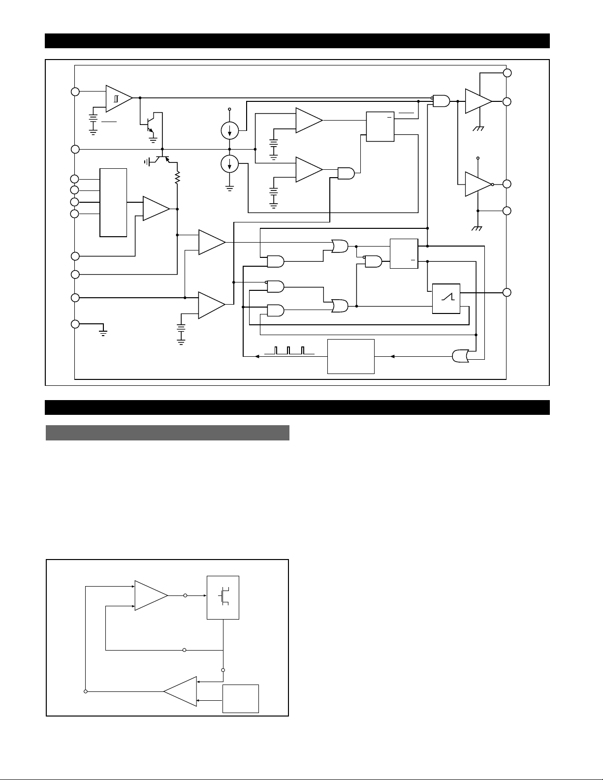
Block Diagram
V
Applications Information
V
2
™
Control Method
The V
2
™
method of control uses a ramp signal that is generated by the ESR of the output capacitors. This ramp is
proportional to the AC current through the main inductor
and is offset by the value of the DC output voltage. This
control scheme inherently compensates for variation in
either line or load conditions, since the ramp signal is generated from the output voltage itself. This control scheme
differs from traditional techniques such as voltage mode,
which generates an artificial ramp, and current mode,
which generates a ramp from inductor current.
Figure 1: V
2
™
Control Diagram
The V
2
™
control method is illustrated in Figure 1. The output voltage is used to generate both the error signal and the
ramp signal. Since the ramp signal is simply the output
voltage, it is affected by any change in the output regardless of the origin of that change. The ramp signal also contains the DC portion of the output voltage, which allows
the control circuit to drive the main switch to 0% or 100%
duty cycle as required.
A change in line voltage changes the current ramp in the
inductor, affecting the ramp signal, which causes the V
2
™
control scheme to compensate the duty cycle. Since the
change in inductor current modifies the ramp signal, as in
current mode control, the V
2
™
control scheme has the
same advantages in line transient response.
A change in load current will have an affect on the output
voltage, altering the ramp signal. A load step immediately
changes the state of the comparator output, which controls
the main switch. Load transient response is determined
only by the comparator response time and the transition
speed of the main switch. The reaction time to an output
load step has no relation to the crossover frequency of the
error signal loop, as in traditional control methods.
The error signal loop can have a low crossover frequency,
since transient response is handled by the ramp signal loop.
The main purpose of this ‘slow’ feedback loop is to provide
DC accuracy. Noise immunity is significantly improved,
since the error amplifier bandwidth can be rolled off at a low
frequency. Enhanced noise immunity improves remote sens-
Theory of Operation
CC1
SS
V
ID0
V
ID1
V
ID2
V
ID3
V
COMP
V
FFB
LGnd
V
Monitor
CC1
Comparator
-
60µA
2µA
-
+
-
+
V
FFB
Comparator
5V
2.5V
Low
+
3.90V
3.85V
4 BIT
DAC
FB
Slow Feedback
Fast Feedback
+
-
Error
Amplifier
PWM
Comparator
1V
0.7V
-
+
+
-
Maximum
On-Time
Timeout
Normal
Off-Time
Timeout
Extended
Off-Time
Timeout
SS Low
Comparator
SS High
Comparator
R
S
FAULT
Latch
Off-Time
Timeout
FAULT
Q
FAULT
Q
V
CC1
Q
Q
GATE(H) = ON
GATE(H) = OFF
C
OFF
One Shot
R
S
Q
R
S
PWM
Latch
PGnd
V
CC2
V
GATE(H)
V
GATE(L)
PGnd
C
OFF
PWM
COMP
COMP
PWM
Comparator
+
C
–
Ramp
Signal
Error
Signal
V
Error
Amplifier
GATE(H)
V
GATE(L)
V
FFB
Output
Voltage
Feedback
V
FB
–
E
+
Reference
Voltage
Time Out
Timer
(30µs)
Edge Triggered
 Loading...