

CHERRY Semiconductor CS5132 Service Manual
The CS5132 is a dual output CPU
power supply controller. It contains a synchronous dual NFET
buck controller utilizing the V
2
TM
control method to achieve the
fastest possible transient response
and best overall regulation. The
CS5132 also contains a second nonsynchronous NFET buck controller. These synchronous and
non-synchronous buck regulators
are designed to power the core and
I/O logic of the latest high performance CPUs. The CS5132 incorporates many additional features
required to ensure the proper
operation and protection of the
CPU and power system. The
CS5132 dual output provides the
industryÕs most highly integrated
solution, minimizing external component count, total solution size,
and cost.
The CS5132 is specifically designed
to power IntelÕs Pentium¨II processor and includes the following
features: 5 bit DAC and fixed
1.23V reference, Power-Good output, hiccup mode overcurrent protection, adaptive voltage positioning, and overvoltage protection.
The CS5132 will operate over an
8.4V to 14V range and is available
in 24 lead surface mount package.
1
Features
■ Synchronous Switching
Regulator Controller (V
CORE
)
■ Dual N-Channel MOSFET
Synchronous Buck Design
■ V
2
TM
Control Topology
■ 200ns Transient Loop Response
■ 5 bit DAC with 1% Tolerance
■ Hiccup Mode Overcurrent
Protection
■ 65ns adaptive FET Non-Overlap
Time
■ Non-Synchronous Switching
Regulator Controller (V
I/O
)
■ Single N-Channel MOSFET
buck design
■ Adjustable Output with 2%
Tolerance
■ System Power Management
Pentium
¨
II System V
CORE
and V
I/O
Controlled by
a Single IC
Power-Good Output
Monitors V
CORE
Switching
Regulator Output
OVP Signal Monitors V
CORE
Switching Regulator Output
Package Options
CS5132
Dual Output CPU Buck Controller
CS5132
Description
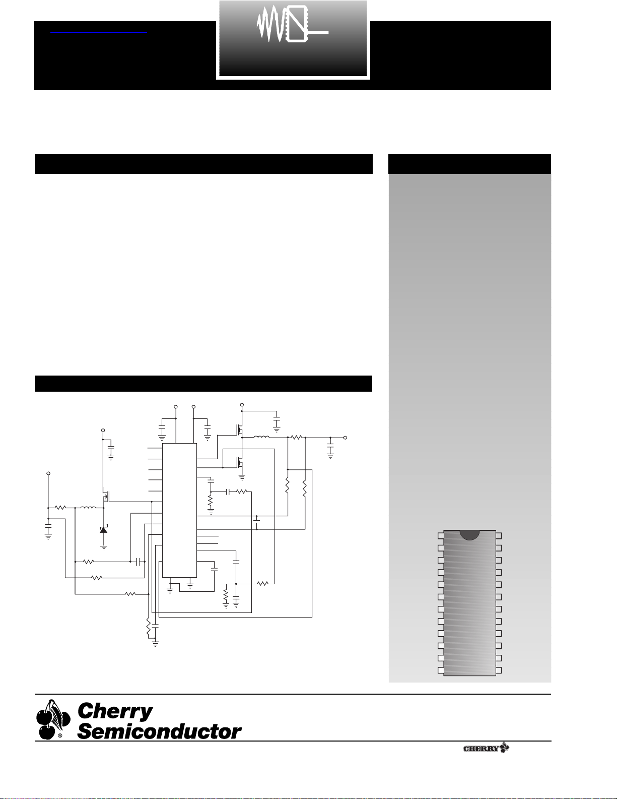
Application Diagram
16
15
14
13
12
11
10
1
2
3
4
5
6
7
8
V
ID2
V
ID3
V
ID4
C
OFF1
COMP1
V
OUT1
V
FB1
V
FFB1
V
ID1
V
ID0
PWRGD
OVP
V
CC1
GATEL
PGND
GATEH
LGND V
CC2
9
17
18
V
FFB2
GATE
19
20
V
FB2
C
OFF2
V
OUT2
COMP2
21
22
23
24
24L SO Wide
5V/12V to 2V/16A for Pentium¨II V
CC(CORE)
, 5V/12V to 3.3V/8A for V
I/O
Pentium is a registered trademark of Intel Corporation.
V
2
is a trademark of Switch Power, Inc.
Rev. 11/3/98
Cherry Semiconductor Corporation
2000 South County Trail, East Greenwich, RI 02818
Tel: (401)885-3600 Fax: (401)885-5786
Email: info@cherry-semi.com
Web Site: www.cherry-semi.com
A Company
¨
查询CS5132供应商
+5V
C3-C5
1200mF x 3
10V
+3.3V (V
)
I/O
L2
3.5mH
510W
Q3
FS70VSJ-03
MBRD835L
D1
R2
R6
510W
C17
0.1mF
R3
2K
1%
R4
1.18K
1%
PCB TRACE
(FreeCurrent
Sensing Element)
6.6mW
C18-C21
1200mF
10V
x 4
+12V
C2
1mF
20
23
V
ID0
24
V
ID1
1
V
ID2
2
V
ID3
3
V
ID4
15
GATE
10
V
FFB2
12
V
OUT2
11
V
FB2
14
C
OFF2
7
V
FB1
LGnd
9
C16
390pF
V
CC1VCC2
GATE(H)
GATE(L)
COMP2
PWRGD
COMP1
+12V
16
17
19
13
51W
8
V
FFB1
6
V
OUT1
22
21
OVP
5
4
C
OFF1
PGnd
18
+5V
Q1
C1
1mF
Q2
C12
0.1mF
C22
10K
100pF
R8
C15
680pF
0.01mF
100W
R10 C25
FS70VSJ-03
FS70VSJ-03
R7
C14
0.1mF
1.2mH
L1
R9
10K
C13
0.1mF
C6-C11
1200mF x 6
10V
R1
510W
PCB TRACE (Free
Current Sensing
Element)
3.3mW
R5
510W
C23-C30
1200mF x 8
10V
V
CC(CORE)

2
CS5132
Package Pin Description
PACKAGE PIN # PIN SYMBOL FUNCTION
Absolute Maximum Ratings
Pin Symbol Pin Name
V
MAX
V
MIN
I
SOURCE
I
SINK
V
CC1
IC Logic and Low Side Driver Power Input 16V -0.3V N/A 1.5A Peak
200mA DC
V
CC2
IC High Side Drivers Power Input 16V -0.3V N/A 3A Peak
400mA DC
COMP1, COMP2 Compensation Pins for the V
CORE
6V -0.3V 1mA 5mA
and V
I/O
error amplifiers.
V
FB1
, V
OUT1
, V
ID0-4
, V
CORE
Voltage Feedback Input Pin,
V
OUT2
, V
FB2
, V
FFB1
, V
CORE
Output Voltage Sense Pin,
V
FFB2
Voltage ID DAC Input Pins, V
I/O
Output Voltage 6V -0.3V 1mA 1mA
Sense Pin, V
I/O
Voltage Feedback Input Pin,
V
CORE
PWM comparator Fast Feedback Pin, V
I/O
PWM comparator Fast Feedback Pin.
C
OFF1
, C
OFF2
Off-Time Pins for the V
CORE
and V
I/O
regulators 6V -0.3V 1mA 50mA
GATE(H), GATE High-Side FET Drivers for the V
CORE
16V -0.3V 1.5A Peak 1.5A Peak
and V
I/O
regulators. 200mA DC 200mA DC
GATE(L) Low-Side FET Driver 16V -0.3V 1.5A Peak 1.5A Peak
200mA DC 200mA DC
PWRGD Power-Good Output 6V -0.3V 1mA 30mA
OVP Overvoltage Protection 15V -0.3V 30mA 1mA
PGnd Power Ground 0V 0V 3A Peak N/A
400mA DC
LGnd Logic Ground 0V 0V 40mA N/A
23,24,1,2,3 V
IDO
Ð V
ID4
Voltage ID DAC inputs. These pins are internally pulled up to 5.65V if
left open. V
ID4
selects the DAC range. When V
ID4
is high (logic one),
the Error Amp reference range is 2.125V to 3.525V with 100mV increments. When V
ID4
is low (logic zero), the Error amp reference voltage
is 1.325V to 2.075V with 50mV increments.
20 V
CC1
Input power supply pin for the internal circuitry, and low side gate
driver. Decouple with filter capacitor to PGnd.
17 GATE(H) High side switch FET driver pin for V
CORE
section.
18 PGnd Power ground for V
CORE
and V
I/O
section.
19 GATE(L) Low side synchronous FET driver pin.
16 V
CC2
Input power supply pin for on-board high side gate drivers. Decouple
with filter capacitor to PGnd.
15 GATE High side switch FET driver pin for V
I/O
section.
21 OVP Overvoltage protection pin. Goes high when overvoltage condition is
detected on V
FB1
.
22 PWRGD Power-Good Output. Open collector output drives low when V
FB1
is
out of regulation.
Operating Junction Temperature, T
J
. . . . . . . . . . . . . . . . . . . . . . . . . . . . . . . . . . . . . . . . . . . . . . . . . . . . . . . . . . . . . 0 to 125¡C
Lead Temperature Soldering:
Reflow (SMD styles only) . . . . . . . . . . . . . . . . . . . . . . . . . . . . . . . . . . . . . . . . . . 60 sec max. above 183ûC, 230ûC Peak
Storage Temperature Range, TS. . . . . . . . . . . . . . . . . . . . . . . . . . . . . . . . . . . . . . . . . . . . . . . . . . . . . . . . . . . . . . . . -65 to 150ûC
ESD Susceptibility . . . . . . . . . . . . . . . . . . . . . . . . . . . . . . . . . . . . . . . . . . . . . . . . . . . . . . . . . . . . . . . . . . . . . . . . . . . . . . . Class 2
3
CS5132
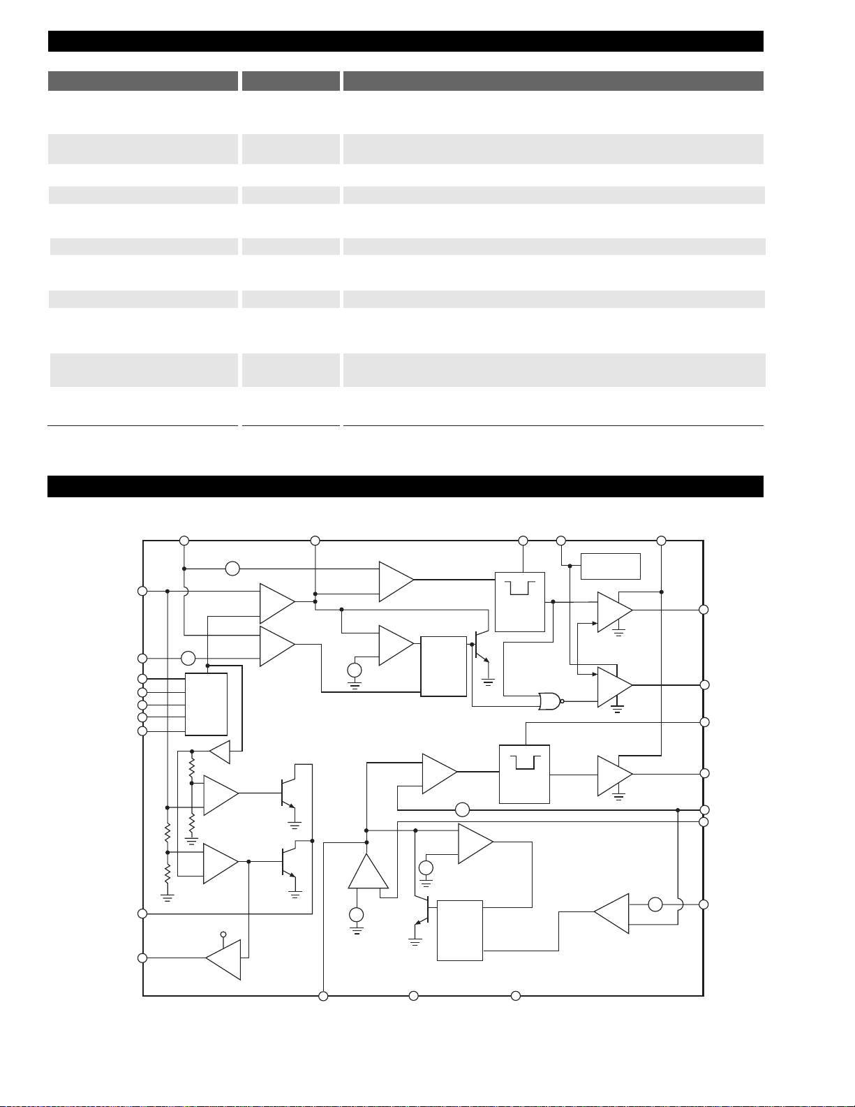
Block Diagram
PACKAGE PIN # PIN SYMBOL FUNCTION
Package Pin Description: continued
14 C
OFF2
Off-Time Capacitor Pin. A capacitor from this pin to LGnd sets the off
time for the non-synchronous regulator (V
I/O
).
13 COMP2 V
I/O
section error amp output. PWM comparator inverting input. A
capacitor to LGnd provides error amp compensation.
12 V
OUT2
V
I/O
section current limit comparator inverting input.
11 V
FB2
V
I/O
section error amp inverting feedback input.
10 V
FFB2
V
I/O
PWM comparator fast feedback non-inverting input. V
I/O
sec-
tion current limit comparator non-inverting input.
9 LGnd Logic ground.
7V
FB1
V
CORE
section error amp inverting input, PWRGD and OVP compara-
tor input.
6V
OUT1
V
CORE
section current limit comparator inverting input.
5 COMP1
V
CORE
section error amp output. V
CORE
section PWM comparator
inverting input. A capacitor to LGnd provides error amp compensation.
4C
OFF1
Off-Time Capacitor Pin. A capacitor from this pin to LGnd sets the off
time for the synchronous regulator (V
CORE
).
8V
FFB1
V
CORE
section PWM comparator fast feedback non-inverting input.
V
CORE
section current limit comparator non-inverting input.
V
FFB1
+
-
86mV
+
-
DAC
V
CC1
1.06V
+
-
+
-
V
FB1
V
OUT1
VID0
VID1
VID2
VID3
VID4
PWRGD
OVP
COMP1
EA1
-
+
Current
Limit1
+
-
+
C
OFF1VCC1
V
CC2
-
+
+
-
0.25V
EA2
1.23V
+
-
Discharge
Comparator
-
+
-
PWM
COMP1
R
Latch1
S
-
+
+
-
Fault
PWM
COMP2
0.25V
Q
Latch2
Q
1.10V
+
-
+
Fault
-
Discharge
Comparator
R
S
Off Time1
One Shot
Off Time2
One Shot
UVLO
Non-overlap
Logic
Current
Limit2
PGnd
PGnd
PGnd
-
+
86mV
+
GATE(H)
GATE(L)
C
OFF2
GATE
V
FFB2
V
FB2
-
V
OUT2
LGndCOMP2
PGnd
4
CS5132
Electrical Characteristics: 0ûC < TA< 70ûC; 0ûC < TJ< 125ûC; V
OUT2
² 3.5V, 9V ² V
CC1
² 14V, 9V ² V
CC2
² 14V; 2.0V DAC Code
(V
ID4
= V
ID3
= V
ID2
= V
ID1
= 0, V
ID0
= 1), C
GATE(H)
= C
GATE(L)
= C
GATE
= 3.3nF, C
OFF
= 390pF; Unless otherwise stated.
PARAMETER TEST CONDITIONS MIN TYP MAX UNIT
■ V
CORE
Switching Regulator Error Amplifier
V
FB1
Bias Current V
FB1
= 0V -1.0 0.1 1.0 µA
COMP1 Source Current COMP1 = 1.2V to 3.6V; V
FB1
= 1.9 V 15 30 60 µA
COMP1 Sink Current COMP1=1.2V; V
FB1
=2.1V; 30 60 120 µA
Open Loop Gain C
COMP1
= 0.1µF 80 dB
Unity Gain Bandwidth C
COMP1
= 0.1µF 20 kHz
PSRR @ 1kHz C
COMP1
= 0.1µF 70 dB
■ Voltage Identification DAC
Accuracy (all codes) Measure V
FB1
= COMP1,
25ûC ² T
J
² 125ûC, V
CC1
= V
CC2
= 12V -1.0 1.0 %
V
ID4VID3VID2VID1VID0
1 0 0 0 0 3.489 3.525 3.560 V
1 0 0 0 1 3.390 3.425 3.459 V
1 0 0 1 0 3.291 3.325 3.358 V
1 0 0 1 1 3.192 3.225 3.257 V
1 0 1 0 0 3.093 3.125 3.156 V
1 0 1 0 1 2.994 3.025 3.055 V
1 0 1 1 0 2.895 2.925 2.954 V
1 0 1 1 1 2.796 2.825 2.853 V
1 1 0 0 0 2.697 2.725 2.752 V
1 1 0 0 1 2.598 2.625 2.651 V
1 1 0 1 0 2.499 2.525 2.550 V
1 1 0 1 1 2.400 2.425 2.449 V
1 1 1 0 0 2.301 2.325 2.348 V
1 1 1 0 1 2.202 2.225 2.247 V
1 1 1 1 0 2.103 2.125 2.146 V
0 0 0 0 0 2.054 2.075 2.096 V
0 0 0 0 1 2.004 2.025 2.045 V
0 0 0 1 0 1.955 1.975 1.995 V
0 0 0 1 1 1.905 1.925 1.944 V
0 0 1 0 0 1.856 1.875 1.894 V
0 0 1 0 1 1.806 1.825 1.843 V
0 0 1 1 0 1.757 1.775 1.793 V
0 0 1 1 1 1.707 1.725 1.742 V
0 1 0 0 0 1.658 1.675 1.692 V
0 1 0 0 1 1.608 1.625 1.641 V
0 1 0 1 0 1.559 1.575 1.591 V
0 1 0 1 1 1.509 1.525 1.540 V
0 1 1 0 0 1.460 1.475 1.490 V
0 1 1 0 1 1.410 1.425 1.439 V
0 1 1 1 0 1.361 1.375 1.389 V
0 1 1 1 1 1.311 1.325 1.338 V
1 1 1 1 1 1.225 1.250 1.275 V
Line Regulation 9V ² V
CC1
² 14V 0.01 %/V
Input Threshold V
ID4
, V
ID3
, V
ID2
, V
ID1
, V
ID0
1.00 1.25 2.40 V

5
CS5132
PARAMETER TEST CONDITIONS MIN TYP MAX UNIT
Electrical Characteristics: 0ûC < TA< 70ûC; 0ûC < TJ< 125ûC; V
OUT2
² 3.5V, 9V ² V
CC1
² 14V, 9V ² V
CC2
² 14V; 2.0V DAC Code
(V
ID4
= V
ID3
= V
ID2
= V
ID1
= 0, V
ID0
= 1), C
GATE(H)
= C
GATE(L)
= C
GATE
= 3.3nF, C
OFF
= 390pF; Unless otherwise stated.
Input Pull-up Resistance V
ID4
, V
ID3
, V
ID2
, V
ID1
, V
ID0
25 50 100 k½
Pull-up Voltage 5.48 5.65 5.82 V
■ GATE(H) and GATE(L)
High Voltage at 100mA Measure V
CC1/2
ÐGATE(L)/(H) 1.2 2.1 V
Low Voltage at 100mA Measure GATE(L)/(H) 1.0 1.5 V
Rise Time 1.6V < GATE(H)/(L) < (V
CC1/2
Ð 2.5V) 40 80 ns
Fall Time (V
CC1/2
Ð 2.5V) > GATE(L)/(H) > 1.6V 40 80 ns
GATE(H) to GATE(L) Delay GATE(H)<2V, GATE(L)>2V 30 65 100 ns
GATE(L) to GATE(H) Delay GATE(L)<2V, GATE(H)>2V 30 65 100 ns
GATE pull-down Resistance to PGnd (Note 1) 20 50 115 k½
■ V
CORE
Overcurrent Protection
OVC Comparator Offset Voltage 0V < V
OUT1
² 3.5V 77 86 101 mV
Discharge Threshold Voltage 0.2 0.25 0.3 V
V
OUT1
Bias Current 0.2V ² V
OUT1
² 3.5V -7.0 0.1 7.0 µA
OVC Latch Discharge Current V
COMP
= 1V 100 800 2500 µA
■ PWM Comparator 1
PWM Comparator Offset Voltage 0V ² V
FFB1
² 3.5V 0.95 1.06 1.18 V
Transient Response V
FFB1
= 0 to 3.5V 200 300 ns
V
FFB1
Bias Current 0.2V ² V
FFB1
² 3.5V -7.0 0.1 7.0 µA
■ C
OFF1
Off-Time 1.0 1.6 2.3 µs
Charge Current V
COFF1
= 1.5V 550 µA
Discharge Current V
COFF1
= 1.5V 25 mA
■ Power-Good Output
PWRGD Sink Current V
FB1
= 1.7V, V
PWRGD
= 5V 0.5 4 15 mA
PWRGD Upper Threshold % of nominal DAC code 5 8.5 12 %
PWRGD Lower Threshold % of nominal DAC code -12 -8.5 -5 %
PWRGD Output Low Voltage V
FB1
= 1.7V, I
PWRGD
= 500µA 0.2 0.3 V
■ Overvoltage Protection (OVP) Output
OVP Source Current OVP = 1V 1 10 25 mA
OVP Threshold % of nominal DAC code 5 8.5 12 %
OVP Pull-up Voltage I
OVP
= 1mA, V
CC1
- V
OVP
1.1 1.5 V
■ V
I/O
Switching Regulator Error Amplifier
V
FB2
Bias Current V
FB2
= 0V -1.0 0.1 1.0 µA
COMP2 Source Current COMP2 = 1.2V to 3.6V; V
FB2
= 1V 15 30 60 µA
COMP2 Sink Current COMP2=1.2V; V
FB2
=1.4V; 30 60 120 µA
Open Loop Gain C
COMP2
= 0.1µF 80 dB
CS5132
PARAMETER TEST CONDITIONS MIN TYP MAX UNIT
Electrical Characteristics: 0ûC < TA< 70ûC; 0ûC < TJ< 125ûC; V
OUT2
3.5V, 9V V
CC1
14V, 9V V
CC2
14V; 2.0V DAC Code
(V
ID4
= V
ID3
= V
ID2
= V
ID1
= 0, V
ID0
= 1), C
GATE(H)
= C
GATE(L)
= C
GATE
= 3.3nF, C
OFF
= 390pF; Unless otherwise stated.
6
■ V
I/O
Switching Regulator Error Amplifier continued
Unity Gain Bandwidth C
COMP2
= 0.1µF 20 KHz
PSRR @ 1kHZ C
COMP2
= 0.1µF 70 dB
Reference Voltage V
FB2
=COMP2 1.205 1.230 1.255 V
■ GATE
High Voltage at 100mA Measure V
CC2
ÐGATE 1.2 2.1 V
Low Voltage at 100mA Measure GATE 1.0 1.5 V
Rise Time 1.6V < GATE < (V
CC2
Ð 2.5V) 40 80 ns
Fall Time (V
CC2
Ð 2.5V) > GATE > 1.6V 40 80 ns
GATE pull-down Resistance to PGnd 20 50 115 k½
■ V
I/O
Overcurrent Protection
OVC2 Comparator Offset Voltage 0V < V
OUT2
² 3.5V 77 86 101 mV
Discharge Threshold Voltage 0.2 0.25 0.3 V
V
OUT2
Bias Current 0.2V ² V
OUT2
² 3.5V -7.0 0.1 7.0 µA
OVC2 Latch Discharge Current 100 800 2500 µA
■ PWM Comparator 2
PWM Comparator Offset Voltage 0V ² V
FFB2
² 3.5V 0.99 1.10 1.22 V
Transient Response V
FFB2
= 0 to 3.5V 200 300 ns
V
FFB2
Bias Current 0.2V ² V
FFB2
² 3.5V -7.0 0.1 7.0 µA
■ C
OFF2
Off-Time 1.0 1.6 2.3 µs
Charge Current V
COFF2
= 1.5V 550 µA
Discharge Current V
COFF2
= 1.5V 25 mA
■ General Electrical Specifications
V
CC
Monitor Start Threshold All Outputs On 7.9 8.4 8.9 V
V
CC
Monitor Stop Threshold All Outputs Off 7.6 8.1 8.6 V
Hysteresis Start - Stop 0.15 0.30 0.60 V
V
CC1
Supply Current No Load on GATE(L) 13 20 mA
V
CC2
Supply Current No Loads on GATE(H) and GATE 6 9 mA
Note 1: Guaranteed by design, not 100% tested in production.
 Loading...