

CHERRY Semiconductor CS51312 Service Manual
Features
■ Synchronous Switching
Regulator Controller for CPU
V
CORE
■ Dual N-Channel MOSFET
Synchronous Buck Design
■ V
2
TM
Control Topology
■ 200ns Transient Loop Response
■ 5 bit DAC with 1.2% Tolerance
■ Hiccup Mode Overcurrent
Protection
■ 40ns Gate Rise and Fall Times
(3.3nF load)
■ 65ns Adaptive FET Non-overlap
Time
■ Adaptive Voltage Positioning
■ Power-Good Output Monitors
Regulator Output
■ 5V/12V or 12V-only Operation
■ V
CC
Monitor Provides Under
Voltage Lockout
■ OVP Output Monitors Regulator
Output
■ Multifunction COMP Pin
Provides ENABLE, Soft Start,
and Hiccup Timing in
Addition to Control Loop
Compensation
Package Options
CS51312
Synchronous CPU Buck Controller
for 12V Only Applications
CS51312
Description
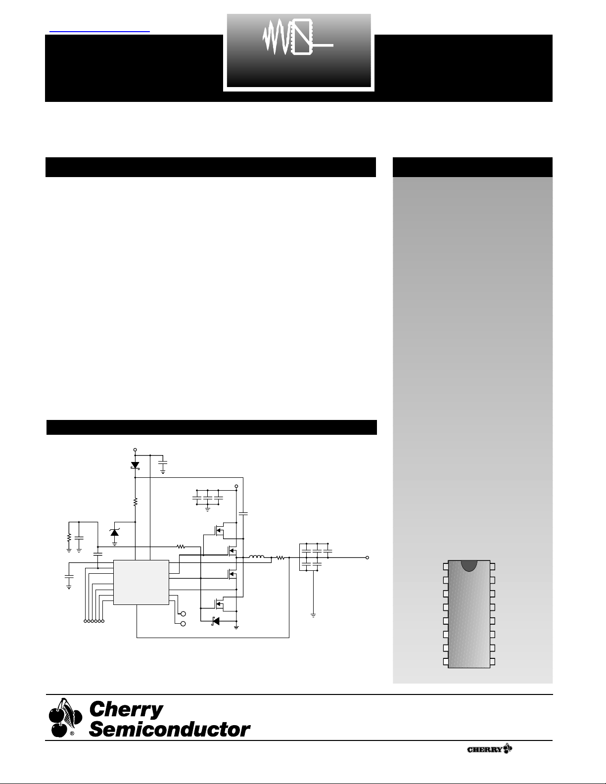
Application Diagram
GATE(H)V
OUT
VID0
VID1
VID2
VID3
VID4
V
FB
V
CC2
PWRGD
OVP
GATE(L)
Gnd
COMP
C
OFF
V
CC1
16 Lead SO Narrow
1
Pentium is a registered trademark of Intel Corporation.
A Company
®
V2is a trademark of Switch Power, Inc.
Rev. 3/11/99
Cherry Semiconductor Corporation
2000 South County Trail, East Greenwich, RI 02818
Tel: (401)885-3600 Fax: (401)885-5786
Email: info@cherry-semi.com
Web Site: www.cherry-semi.com
12V to 16A high performance converter.
The CS51312 is a synchronous dual
NFET Buck Regulator Controller. It is
designed to power the core logic of
the latest high performance CPUs and
ASICs from a single 12V input. It uses
the V
2
TM
control method to achieve
the fastest possible transient response
and best overall regulation. It incorporates many additional features
required to ensure the proper operation and protection of the CPU and
Power system. The CS51312 provides
the industry’s most highly integrated
solution, minimizing external component count, total solution size, and
cost.
The CS51312 is specifically designed
to power Intel’s Pentium
®
II processor
and includes the following features:
5-bit DAC with 1.2% tolerance,
Power-Good output, overcurrent hiccup mode protection, overvoltage
protection, V
CC
monitor, Soft Start,
adaptive voltage positioning, adaptive FET non-overlap time, and
remote sense. The CS51312 will operate over a 9V to 20V (V
CC2
) range
using either single or dual input voltage and is available in 16 lead narrow
body surface mount package.
R2
200
C9
0.01µF
C10
1µF
C19
1000pF
12V
C1
1.0µF
D1
SS16GICT-ND
R1
22Ω
D2
ZM4746ACT-ND
V
ID4
V
ID3
V
ID2
V
ID1
C
OFF
COMP
V
ID0
V
CC2VCC1
V
FB
GATE(H)
GATE(L)
Gnd
OVP
PWRGDV
OUT
CS51312
12V
C2 C3 C4
220µF
16SV220
C6
0.010µF
FY10AAJ-03A
FY10AAJ-03A
Q1
Q2
Q3
FY10AAJ-03A
FY10AAJ-03A
Q4
D3
SS12GICT-ND
OVP
PWRGD
R3
10k
L1
1.2µH
R4
0.004Ω
C14 C15
470µF
C11 C12 C13
470µF
1.25V to 3.5V
T510X477K006AS4394
98
6
10
12
11
13
14
15
16
1
2
3
4
5
7
1
DAC
ENABLE
+++
+++
++
1
查询CS51312供应商
1

2
Package Pin Description
PACKAGE PIN # PIN SYMBOL FUNCTION
Absolute Maximum Ratings
Pin Symbol Pin Name
V
MAX
V
MIN
I
SOURCE
I
SINK
CS51312
Operating Junction Temperature, TJ . . . . . . . . . . . . . . . . . . . . . . . . . . . . . . . . . . . . . . . . . . . . . . . . . . . . . . . . . . . . . . . 150°C
Lead Temperature Soldering
Reflow (SMD styles only) . . . . . . . . . . . . . . . . . . . . . . . . . . . . . . . . . . . . . . . . . . .60 sec. max above 183°C, 230°C peak
Storage Temperature Range, TS . . . . . . . . . . . . . . . . . . . . . . . . . . . . . . . . . . . . . . . . . . . . . . . . . . . . . . . . . . . . . -65° to 150°C
ESD Susceptibility . . . . . . . . . . . . . . . . . . . . . . . . . . . . . . . . . . . . . . . . . . . . . . . . . . . . . . . . . . . . . . . . . . . . . . . . . . . . . . . . 2kV
V
CC1
IC Bias and Low Side Driver 16V -0.3V N/A 1.5A Peak
Power Input 200mA
V
CC2
IC High Side Driver Power Input 20V -0.3V N/A 1.5A Peak
200mA
COMP Compensation Pin 6V -0.3V 1mA 5mA
V
FB
, V
OUT
, V
ID0-4
Voltage Feedback Input, Output 6V -0.3V 1mA 1mA
Voltage Sense Pin, Voltage
ID DAC Inputs
C
OFF
Off-Time Pin 6V -0.3V 1mA 50mA
GATE(H) High-Side FET Driver 20V -0.3V DC 1.5APeak 1.5A Peak
GATE(L) Low-Side FET Driver 16V 200mA DC 200mA DC
PWRGD Power-Good Output 6V -0.3V 1mA 30mA
OVP Overvoltage Protection 15V -0.3V 30mA 1mA
Gnd Ground 0V 0V 1.5A Peak N/A
200mA DC
1,2,3,4,5 V
IDO
– V
ID4
Voltage ID DAC inputs. These pins are internally pulled up to
5.65V if left open. V
ID4
selects the DAC range. When V
ID4
is
high (logic one), the Error Amp reference range is 2.125V to
3.525V with 100mV increments. When V
ID4
is low (logic zero),
the Error amp reference voltage is 1.325V to 2.075V with 50mV
increments.
6V
FB
Error amp inverting input, PWM comparator non-inverting
input, current limit comparator non-inverting input, PWRGD
and OVP comparator input.
7V
OUT
Current limit comparator inverting input.
8V
CC1
Input power supply pin for the internal circuitry and low side
gate driver. Decouple with filter capacitor to Gnd.
9V
CC2
Input power supply pin for the high side gate driver.
Decouple with filter capacitor to Gnd.
10 GATE(H) High side switch FET driver pin .
11 Gnd Ground pin and IC substrate connection.
12 GATE(L) Low side synchronous FET driver pin.
13 OVP Overvoltage protection pin. Drives high when overvoltage
condition is detected on V
FB
.
14 PWRGD Power-Good Output. Open collector output drives low when
V
FB
is out of regulation.
15 C
OFF
Off-Time Capacitor Pin. A capacitor from this pin to Gnd sets
the off time for the regulator
16 COMP Error amp output. PWM comparator inverting input.
A capacitor on this pin provides error amp compensation, and
determines the Soft Start and hiccup timing. Pulling COMP
below 1.1V (typ) turns off both GATE drivers and shuts down
the regulator.
Electrical Characteristics: 0˚C < TA< 70˚C; 0˚C < TJ< 125˚C; 9V < V
CC1
< 14V; 9V ≤ V
CC2
≤ 20V;
2.0V DAC Code(V
ID4
= V
ID3=VID2
= V
ID1
= 0, V
ID0
= 1), C
GATE(H)
= C
GATE(L)
= 3.3nF, C
OFF
= 390pF; Unless otherwise stated.
PARAMETER TEST CONDITIONS MIN TYP MAX UNIT
3
CS51312
■ Voltage Identification DAC
Measure VFB= V
COMP
, VCC= 12V (Note 1)
75°C ≤ TJ≤ 125°C 25°C ≤ TJ≤ 75°C
V
ID4VID3VID2VID1VID0
MIN TYP MAX ± TOL MIN TYP MAX ± TOL UNIT
■ Error Amplifier
V
FB
Bias Current 0.2V ≤VFB≤ 3.5V -7.0 0.1 7.0 µA
COMP Source Current V
COMP
= 1.2V to 3.6V; VFB= 1.9 V 15 30 60 µA
COMP Sink Current V
COMP
=1.2V; VFB= 2.1V; 30 60 120 µA
Open Loop Gain C
COMP
= 0.1µF 80 dB
Unity Gain Bandwidth C
COMP
= 0.1µF 50 kHz
PSRR @ 1kHz C
COMP
= 0.1µF 70 dB
Transconductance 32 mmho
Output Impedance 0.5 MΩ
10000 3.483 3.525 3.567 1.2% 3.455 3.525 3.596 2.0% V
10001 3.384 3.425 3.466 1.2% 3.357 3.425 3.494 2.0% V
10010 3.285 3.325 3.365 1.2% 3.259 3.325 3.392 2.0% V
10011 3.186 3.225 3.264 1.2% 3.161 3.225 3.290 2.0% V
10100 3.087 3.125 3.163 1.2% 3.063 3.125 3.188 2.0% V
10101 2.989 3.025 3.061 1.2% 2.965 3.025 3.086 2.0% V
10110 2.890 2.925 2.960 1.2% 2.875 2.925 2.975 1.7% V
10111 2.791 2.825 2.859 1.2% 2.777 2.825 2.873 1.7% V
11000 2.692 2.725 2.758 1.2% 2.679 2.725 2.771 1.7% V
11001 2.594 2.625 2.657 1.2% 2.580 2.625 2.670 1.7% V
11010 2.495 2.525 2.555 1.2% 2.482 2.525 2.568 1.7% V
11011 2.396 2.425 2.454 1.2% 2.389 2.425 2.461 1.5% V
11100 2.297 2.325 2.353 1.2% 2.290 2.325 2.360 1.5% V
11101 2.198 2.225 2.252 1.2% 2.192 2.225 2.258 1.5% V
11110 2.099 2.125 2.151 1.2% 2.093 2.125 2.157 1.5% V
00000 2.050 2.075 2.100 1.2% 2.044 2.075 2.106 1.5% V
00001 2.001 2.025 2.049 1.2% 1.995 2.025 2.055 1.5% V
00010 1.953 1.975 1.997 1.1% 1.945 1.975 2.005 1.5% V
00011 1.904 1.925 1.946 1.1% 1.896 1.925 1.954 1.5% V
00100 1.854 1.875 1.896 1.1% 1.847 1.875 1.903 1.5% V
00101 1.805 1.825 1.845 1.1% 1.798 1.825 1.852 1.5% V
00110 1.755 1.775 1.795 1.1% 1.748 1.775 1.802 1.5% V
00111 1.706 1.725 1.744 1.1% 1.699 1.725 1.751 1.5% V
01000 1.656 1.675 1.694 1.1% 1.650 1.675 1.700 1.5% V
01001 1.607 1.625 1.643 1.1% 1.601 1.625 1.649 1.5% V
01010 1.558 1.575 1.593 1.1% 1.551 1.575 1.599 1.5% V
01011 1.508 1.525 1.542 1.1% 1.502 1.525 1.548 1.5% V
01100 1.459 1.475 1.491 1.1% 1.453 1.475 1.497 1.5% V
01101 1.409 1.425 1.441 1.1% 1.404 1.425 1.446 1.5% V
01110 1.360 1.375 1.390 1.1% 1.354 1.375 1.396 1.5% V
01111 1.310 1.325 1.340 1.1% 1.305 1.325 1.345 1.5% V
11111 1.225 1.250 1.275 2.0% 1.225 1.250 1.275 2.0% V

PARAMETER TEST CONDITIONS MIN TYP MAX UNIT
4
CS51312
Electrical Characteristics: 0˚C < TA< 70˚C; 0˚C < TJ< 125˚C; 9V < V
CC1
< 14V; 9V ≤ V
CC2
≤ 20V;
2.0V DAC Code(V
ID4
= V
ID3=VID2
= V
ID1
= 0, V
ID0
= 1), C
GATE(H)
= C
GATE(L)
= 3.3nF, C
OFF
= 390pF; Unless otherwise stated.
Line Regulation 9V ≤ V
CC1
≤ 14V 0.01 %/V
Input Threshold V
ID4
, V
ID3
, V
ID2
, V
ID1
, V
ID0
1.00 1.25 2.40 V
Input Pull-up Resistance V
ID4
, V
ID3
, V
ID2
, V
ID1
, V
ID0
25 50 100 kΩ
Pull-up Voltage 5.48 5.65 5.82 V
■ GATE(H) and GATE(L)
High Voltage at 100mA Measure V
CC1/2
–GATE(L)/(H) 1.2 2.1 V
Low Voltage at 100mA Measure GATE(L)/(H) 1.0 1.5 V
Rise Time 1.6V < GATE(H)/(L) < (V
CC1/2
– 2.5V) 40 80 ns
Fall Time (V
CC1/2
– 2.5V) > GATE(L)/(H) > 1.6V 40 80 ns
GATE(H) to GATE(L) Delay GATE(H)<2V, GATE(L)>2V, V
CC1/2
= 12V 30 65 110 ns
GATE(L) to GATE(H) Delay GATE(L)<2V, GATE(H)>2V,V
CC1/2
= 12V 30 65 110 ns
GATE pull-down Resistance to Gnd (Note 2) 20 50 115 kΩ
■ Overcurrent Protection
OVC Comparator Offset Voltage 0V ≤ V
OUT
≤ 3.5V 77 86 101 mV
Discharge Threshold Voltage 0.2 0.25 0.3 V
V
OUT
Bias Current 0.2V ≤ V
OUT
≤ 3.5V -7.0 0.1 7.0 µA
OVC Latch Discharge Current V
COMP
= 1V 100 800 2500 µA
■ PWM Comparator
PWM Comparator Offset Voltage 0V ≤ V
FB
≤ 3.5V 0.99 1.10 1.23 V
Transient Response V
FB
= 0 to 3.5V 200 300 ns
■ C
OFF
Off-Time 1.0 1.6 2.3 µs
Charge Current V
COFF
= 1.5V 550 µA
Discharge Current V
COFF
= 1.5V 25 mA
■ Power-Good Output
PWRGD Sink Current V
FB
= 1.7V, V
PWRGD
= 1V 0.5 4 15 mA
PWRGD Upper Threshold % of nominal DAC code 5 8.5 12 %
PWRGD Lower Threshold % of nominal DAC code -12 -8.5 -5 %
PWRGD Output Low Voltage V
FB
= 1.7V, I
PWRGD
= 500µA 0.2 0.3 V
■ Overvoltage Protection (OVP) Output
OVP Source Current OVP = 1V 1 10 25 mA
OVP Threshold % of nominal DAC code 5 8.5 12 %
OVP Pull-up Voltage I
OVP
= 1mA, V
CC1
- V
OVP
1.1 1.5 V
CS51312
5
PARAMETER TEST CONDITIONS MIN TYP MAX UNIT
Electrical Characteristics: 0˚C < TA< 70˚C; 0˚C < TJ< 125˚C; 9V < V
CC1
< 14V; 9V ≤ V
CC2
≤ 20V;
2.0V DAC Code(V
ID4
= V
ID3=VID2
= V
ID1
= 0, V
ID0
= 1), C
GATE(H)
= C
GATE(L)
= 3.3nF, C
OFF
= 390pF; Unless otherwise stated.
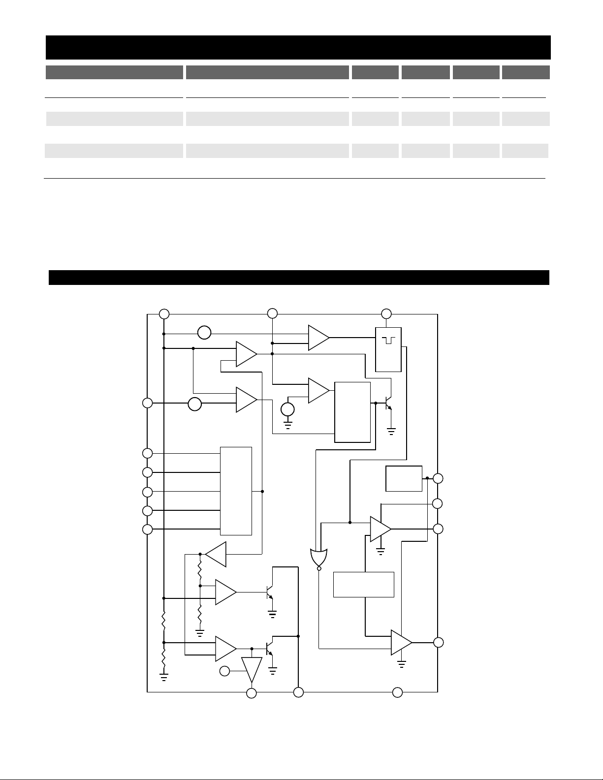
Block Diagram
■ General Electrical Specifications
V
CC1
Monitor Start Threshold 7.9 8.4 8.9 V
V
CC1
Monitor Stop Threshold 7.6 8.1 8.6 V
Hysteresis Start - Stop 0.15 0.30 0.60 V
V
CC1
Supply Current No Load on GATE(H), GATE(L) 9.5 16 mA
V
CC2
Supply Current No Load on GATE(H), GATE(L) 2.5 4.5 mA
Note 1: The IC power dissipation in a typical application with VCC= 12V, switching frequency fSW= 250kHz, 50nc
MOSFETs and R
θJA
= 115°C/W yields an operating junction temperature rise of approximately 52°C, and a junction tem-
perature of 77°C with an ambient temperature of 25°C.
Note 2: Guaranteed by design, not 100% tested in production.
+
-
+
-
+
-
V
FB
COMP
C
OFF
OFF
TIME
PWM COMP
DISCHARGE
COMP
+
-
V
OUT
V
ID0
V
ID1
V
ID2
V
ID3
V
ID4
DAC
+
-
+
-
+
-
1.1V
EA
CURRENT LIMIT
+
-
86mV
0.25V
FAULT
LATCH
R
S
Q
V
CC1
OVP PWRGD Gnd
GATE(L)
GATE(H)
V
CC1
UVLO
NONOVERLAP
LOGIC
+
-
V
CC2
CS51312
6
Application Information
V
2
TM
Control Method
The V
2
TM
method of control uses a ramp signal that is generated by the ESR of the output capacitors. This ramp is
proportional to the AC current through the main inductor
and is offset by the value of the DC output voltage. This
control scheme inherently compensates for variation in
either line or load conditions, since the ramp signal is generated from the output voltage itself. This control scheme
differs from traditional techniques such as voltage mode,
which generates an artificial ramp, and current mode,
which generates a ramp from inductor current.
The V
2
TM
control method is illustrated in Figure 6. The output voltage is used to generate both the error signal and
the ramp signal. Since the ramp signal is simply the output
voltage, it is affected by any change in the output regardless of the origin of that change. The ramp signal also con-
tains the DC portion of the output voltage, which allows
the control circuit to drive the main switch to 0% or 100%
duty cycle as required.
Figure 6: V
2
TM
Control Diagram
Theory Of Operation
Typical Performance Characteristics
150
125
100
75
50
25
0
0 2000 4000 6000 8000 10000 12000 14000 16000
Falltime (ns)
Load Capacitance (pF)
VCC = 12V
T
A
= 25°C
Figure 4: Percent Output Error vs. DAC Output
Voltage Setting, V
ID4
= 0.
Figure 1: Gate(H) and Gate(L) Falltime vs. Load Capacitance.
Figure 2: Gate(H) and Gate(L) Risetime vs. Load Capacitance.
Figure 3: DAC Output Voltage vs. Temperature,
DAC Code = 00001.
0.10
0.05
0
−0.05
−0.10
−0.15
−0.20
1.325 1.375 1.425 1.475 1.525 1.575 1.625 1.675 1.725 1.775 1.825 1.875 1.925 1.975 2.025 2.075
DAC Output Voltage Setting (V)
Output Error (%)
VCC = 12V
T
A
= 25°C
V
ID4
= 0
Figure 5: Percent Output Error vs. DAC Output
Voltage Setting, V
ID4
= 1.
0.35
0.30
0.25
0.20
0.15
0.10
0.05
0
−0.05
−0.10
−0.15
−0.20
−0.25
Output Error (%)
2.125 2.225 2.325 2.425 2.525 2.625 2.725 2.825 2.925 3.025 3.125 3.225 3.335 3.425 3.525
DAC Output Voltage Setting (V)
VCC = 12V
T
A
= 25°C
V
ID4
= 1
150
125
100
75
50
25
0
0 2000 4000 6000 8000 10000 12000 14000 16000
Risetime (ns)
Load Capacitance (pF)
VCC = 12V
T
A
= 25°C
0.10
0.05
0
−0.05
−0.10
−0.15
0 20 40 60 80 100 120
Junction Temperature (°C)
DAC Output Voltage
Deviation (%)
VCC = 12V
COMP
PWM
Comparator
–
+
Ramp Signal
Error
Signal
C
Error
Amplifier
GATE(H)
GATE(L)
E
Output
Voltage
Feedback
V
FB
–
+
Reference
Voltage
 Loading...