

Cherry Semiconductor CS5127GDWR16, CS5127GDW16 Datasheet
Features
■ Nonsynchronous Buck
Design
■ V
2
ª
Control Topology
■ 100ns Transient Loop
Response
■ Programmable Oscillator
Frequency
■ 30ns Typical Gate Rise
and 10ns Fall Times
(No Load)
■ Frequency
Synchronization Input
■ ENABLE Input Controls
Channel 2 Gate Driver
■ 5V/10mA Reference
Output
Package Option
CS5127
Dual Output Nonsynchronous Buck Controller
with Sync Function and Second Channel Enable
CS5127
Description
The CS5127 is a fixed frequency
dual output nonsynchronous buck
controller. It contains circuitry for
regulating two separate outputs.
Each output channel contains a
high gain error amplifier, a comparator and latch, and a totem-pole
output driver capable of providing
DC current of 100mA and peak current in excess of 0.5A. A common
oscillator controls switching for
both channels, and a sync lead is
provided to allow parallel supply
operation or shifting of the switching noise spectrum. An on-chip 5V
reference is capable of providing as
much as 10mA of current for external circuitry. The CS5127 also
contains two undervoltage lockout
circuits. The first lockout releases
when VINreaches 8.4V, while the
second lockout ensures that V
REF
is
higher than 3.6V. The outputs are
held in a low state until both lockouts have released. The controller is
configured to utilize the V
2
ª
control method to achieve the fastest
possible transient response and
best overall regulation. This dual
controller is a cost-effective solution for providing V
CORE
and V
IO
power solutions in computing
applications using a single controller. The CS5127 will operate
over an input voltage range of 9.4V
to 20V and is available in a 16 lead
wide body surface mount package.
Applications Diagram
16 Lead SOIC Wide
1
C
T
SYNC
COMP2
PGND
COMP1
ENABLE
LGND
V
FB1
V
FB2
V
REF
V
IN
GATE1
GATE2
V
FFB1
V
FFB2
R
T
12V, 5V to 2.8V @ 7A and 3.3V @ 7A for 233MHz Pentium¨Processor with MMXª Technology
V2is a trademark of Switch Power, Inc.
Pentium is a registered trademark and MMX is a trademark of Intel Corporation
Rev. 11/3/98
Cherry Semiconductor Corporation
2000 South County Trail, East Greenwich, RI 02818
Tel: (401)885-3600 Fax: (401)885-5786
Email: info@cherry-semi.com
Web Site: www.cherry-semi.com
A Company
¨
C1, C2
2 x 680mF
R2
27k
5V
Q2
IRL3103S
D1
1N5821
+
Q1
FMMT2222ACT
R1
2.8V
20k
1540
1270
0.1mF
R4
R5
C7
330pF
C6
L1
5mH
+
C10, C11
2 x 680mF
C4, C5
+
C8
1mF
IRL3103S
1N5821
+5V
+
C9
0.1mF
Q3
L2
5mH
D2
C12, C13
2 x 680mF
+
SYNC
C
T
R
T
V
FB1
COMP1
V
FFB1
GATE1
LGnd
1mF
CS5127
C3
ENABLE
COMP2
GATE2
V
V
V
FFB2
PGnd
12V
+
2 x 680mF
V
IN
REF
FB2
R9
2k
R3
18k
3.3V
R7
2400
R8
1500
1
R6
1k
R10
20k
C14
330pF
C15
100mF
C16
100mF
C17
330pF
R11
20k

CS5127
2
Absolute Maximum Ratings
Lead Symbol Lead Name
V
MAX
V
MIN
I
SOURCE
I
SINK
Operating Junction Temperature, TJ..................................................................................................................................... 150¡C
Storage Temperature Range, TS...................................................................................................................................-65 to 150¡C
ESD (Human Body Model).........................................................................................................................................................2kV
Lead Temperature Soldering: Reflow (SMD styles only).............................................60 sec. max above 183¡C, 230¡C peak
PARAMETER TEST CONDITIONS MIN TYP MAX UNIT
Electrical Characteristics: 0¡C < TA< 70¡C; 0¡C < TJ< 125¡C; 9.4V < VIN< 20V; CT= 330 pF; RT= 27k½;
unless otherwise stated.
SYNC Oscillator Synchronization Input 5.5V -0.3V 5 mA 5 mA
CT Oscillator Integrating Capacitor 5.5V -0.3V 1mA 1mA
RT Oscillator Charge Current Resistor 5.5V -0.3V 1mA 1mA
V
FB1
, V
FB2
Voltage Feedback Inputs 5.5V -0.3V N/A N/A
COMP1, COMP2 Error Amplifier Outputs 7.5V -0.3V 2mA 50mA
V
FFB1
, V
FFB2
PWM Ramp Inputs 5.5V -0.3V 1mA 1mA
GATE1, GATE2 FET Gate Drive Outputs 20V -0.3V DC, 200mA DC, 200mA DC,
-2.0V for 1A peak 1A peak
t < 50ns (t < 100µs) (t < 100µs)
LGnd Reference Ground and IC Substrate 0V 0V 25 mA N/A
PGnd Power Ground 0V 0V 1A Peak, N/A
200mA DC
ENABLE Channel 2 Enable 5.5V -0.3V 1mA N/A
V
REF
Reference Voltage Output 5.5V -0.3V 150mA 5mA
(short circuit)
V
IN
Power Supply Input 20V -0.3V N/A 200mA DC,
1A peak
(t < 100µs)
■ Reference Section
V
REF
Output Voltage Room Temperature, 4.9 5.0 5.1 V
I
VREF
= 1mA, VIN= 12V
Line Regulation 1 20 mV
Load Regulation 1 mA < I
VREF
< 10 mA 15 26 mV
V
REF
Variation over Line, Load 4.85 5.15 V
and Temperature
Output Short Circuit Current 30 100 150 mA
■ Oscillator Section
Oscillator Frequency Variation 175 210 245 kHz
over Line and Temperature
Maximum Duty Cycle 80 90 98 %
Sync Threshold 0.8 1.6 2.4 V
Sync Bias Current V
SYNC
= 2.4V 170 250 µA
V
SYNC
= 5.0V 430 750
Sync Propagation Delay 230 ns

CS5127
3
PARAMETER TEST CONDITIONS MIN TYP MAX UNIT
Electrical Characteristics: 0¡C < TA< 70¡C; 0¡C < TJ< 125¡C; 9.4V < VIN< 20V; CT= 330 pF; RT= 27k½;
unless otherwise stated.
■ Error Amplifiers
VFBReference Voltage V
COMP
= V
VFB
1.245 1.275 1.300 V
Input Bias Current VFB= 1.275V 0.1 1.0 µA
Open Loop Gain 85 dB
Unity Gain Bandwidth 1.0 MHz
PSRR f = 120Hz 80 dB
COMP Source Current V
COMP
= 3V, V
VFB
= 1.1V 0.9 1.3 2.0 mA
COMP Sink Current V
COMP
= 1.2V, V
VFB
= 1.45V 10 16 24 mA
COMP Output Low Voltage V
VFB
= 1.45V, I
COMP
= 0.3 mA 0.50 0.85 1.00 V
■ PWM Comparators
V
FFB
Bias Current V
FFB
= 0 2.0 20 µA
Propagation Delay V
FFB
rising to V
GATE
falling 100 250 ns
Common Mode 2.9 3.3 V
Maximum Input Voltage
■ ENABLE Lead
ENABLE High Threshold channel 2 enabled 1.5 2.5 3.5 V
ENABLE Bias Current V
ENABLE
= 0 100 250 400 µA
■ Gate Driver Outputs
Output Low Saturation Voltage I
GATE
= 20 mA 0.1 0.4 V
I
GATE
= 100 mA 0.25 2.50 V
Output High Saturation Voltage I
GATE
= 20 mA 1.5 2.0 V
I
GATE
= 100 mA 1.6 3.0 V
Output Voltage under Lockout VIN= 6V, I
GATE
= 1 mA 0.1 0.2 V
Output Rise Time no load 30 ns
Output Fall Time no load 10 ns
■ Undervoltage Lockout
Turn On Threshold 7.4 8.4 9.4 V
Turn Off Threshold 6.8 7.8 8.8 V
■ Supply Current
Start Up Current VIN= 6V 0.4 0.8 mA
Operating Current VCT= 0V, no load 17.5 25 mA

CS5127
4
Package Lead Description
PACKAGE LEAD # LEAD SYMBOL FUNCTION
16 Lead SO Wide
1 SYNC A pulse train on this lead will synchronize the oscillator. Sync threshold level
is 2.4V. Synchronization frequency should be at least 10% higher than the regular operating frequency. The sync feature is level sensitive.
2C
T
The oscillator integrating capacitor is connected to this lead.
3R
T
The oscillator charge current setting resistor is connected to this lead.
4V
FB1
The inverting input of the channel 1 error amplifier is brought out to this lead.
The lead is connected to a resistor divider which provides a measure of the
output voltage. The input is compared to a 1.275V reference, and channel 1
error amp output is used as the V
2
ª
PWM control voltage.
5 COMP1 Channel 1 error amp output and PWM comparator input.
6V
FFB1
This lead connects to the non-inverting input of the channel 1 PWM comparator.
7 GATE1 This lead is the gate driver for the channel 1 FET. It is capable of providing
nearly 1A of peak current.
8 LGND This lead provides a ÒquietÓ ground for low power circuitry in the IC. This
lead should be shorted to the PGND lead as close as possible to the IC for best
operating results.
9 PGND This lead is the power ground. It provides the return path for the FET gate dis-
charge. It should be shorted to the LGND lead as close as possible to the IC for
best operating results.
10 GATE2 This lead is the gate driver for the channel 2 FET. See GATE1 lead description
for more details.
11 V
FFB2
This lead connects to the non-inverting input of the channel 2 PWM comparator.
12 COMP2 Channel 2 error amp output and PWM comparator input.
13 V
FB2
Inverting input for the channel 2 error amp. See V
FBI
for more details.
14 ENABLE The regulator controlled by channel 2 may be turned on and off selectively by
the user. Pulling the ENABLE lead above 3.5V will turn channel 2 on. Setting
the ENABLE lead voltage below 1.5V guarantees that channel 2 is off.
15 V
REF
This lead is the output of a ± 3% reference. This reference drives most of the
on-chip circuitry, but will provide a minimum of 10 mA to external circuitry if
needed. The reference is inherently stable and does not require a compensation capacitor, but use of a decoupling capacitor will reduce noise in the IC.
16 V
IN
This lead is the power supply input to the IC. The maximum input voltage
that can be withstood without damage to the IC is 20V.
CS5127
5
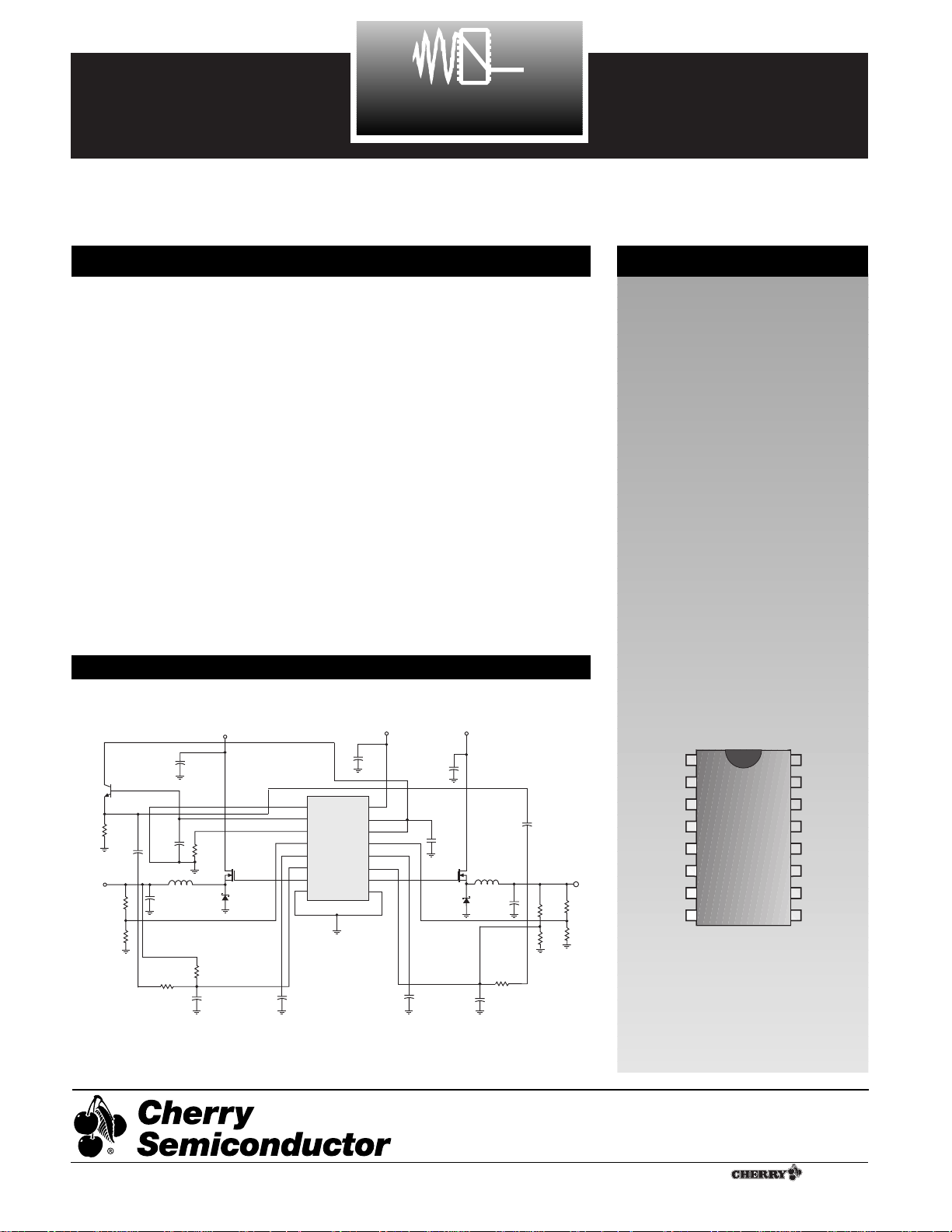
Theory of Operation
The CS5127 is a dual power supply controller that utilizes
the V
2
ª
control method. Two nonsynchronous V
2
ª
buck
regulators can be built using a single controller IC. This IC
is a perfect choice for efficiently and economically providing core power and I/O power for the latest
high-performance CPUs. Both switching regulators
employ a fixed frequency architecture driven from a
common oscillator circuit.
The V
2
ª
method of control uses a ramp signal generated
by the ESR of the output capacitors. This ramp is proportional to the AC current in the inductor and is offset by the
DC output voltage. V
2
ª
inherently compensates for variation in both line and load conditions since the ramp signal
is generated from the output voltage. This differs from traditional methods such as voltage mode control, where an
artificial ramp signal must be generated, and current mode
control, where a ramp is generated from inductor current.
Figure 1: V
2
ª
control diagram.
The V
2
ª
control method is illustrated in Figure 1. Both
the ramp signal and the error signal are generated by the
output voltage. Since the ramp voltage is defined as the
output voltage, the ramp signal is affected by any change
in the output, regardless of the origin of that change. The
ramp signal also contains the DC portion of the output
voltage, allowing the control circuit to drive the output
switch from 0% to about 90% duty cycle.
Changes in line voltage will change the current ramp in
the inductor, affecting the ramp signal and causing the
V
2
ª
control loop to adjust the duty cycle. Since a change
in inductor current changes the ramp signal, the V
2
ª
method has the characteristics and advantages of current
mode control for line transient response.
Changes in load current will affect the output voltage and
thus will also change the ramp signal. A load step will
immediately change the state of the comparator output
that controls the output switch. In this case, load transient
response time is limited by the comparator response time
and the transition speed of the switch. Notice that the reaction time of the V
2
ª
loop to a load transient is not
dependent on the crossover frequency of the error signal
loop. Traditional voltage mode and current mode methods
are dependent on the compensation of the error signal
loop.
The V
2
ª
error signal loop can have a low crossover frequency, since transient response is handled by the ramp
signal loop. The ÒslowÓ error signal loop provides DC
accuracy. Low frequency roll-off of the error amplifier
bandwidth will significantly improve noise immunity.
This also improves remote sensing of the output voltage,
since switching noise picked up in long feedback traces
can be effectively filtered.
V
2
ª
line and load regulation are dramatically improved
because there are two separate control loops. A voltage
V
2
ª
Control Method
Block Diagram
V
FB1
V
REF
V
IN
SYNC
R
C
V
FB2
COMP1
V
FFB1
+
PWM
Comparator
-
Reference
Undervoltage
Lockout
Channel 2
Gate Driver
GATE1
LGND
1.275V
Undervoltage
Lockout
V
-
Error
Amplifier
+
IN
Bandgap
Voltage
Reference
PGND
T
T
1.275V
+
Error
Amplifier
-
Oscillator
-
PWM
Comparator
Channel 2
Gate Driver
GATE2
+
COMP2
+
PWM
Comparator
GATE
-
V
FFB
V
Reference
Voltage
FB
COMP
Ramp Signal
Error
Amplifier
+
Error Signal
-
V
FFB2
ENABLE
CS5127
6
Theory of Operation: continued
mode controller relies on a change in the error signal to
indicate a change in the line and/or load conditions. The
error signal change causes the error loop to respond with a
correction that is dependent on the gain of the error amplifier. A current mode controller has a constant error signal
during line transients, since the slope of the ramp signal
will change in this case. However, regulation of load transients still requires a change in the error signal. V
2
ª
control maintains a fixed error signal for both line and
load variation, since the ramp signal is affected by both.
The CS5127 can be operated in voltage mode if necessary.
For example, if very small values of output ripple voltage
are required, V
2
ª
control may not operate correctly.
Details on how to choose the components for voltage
mode operation are provided in the section on V
FFB
com-
ponent selection.
As output line and load conditions change, the V
2
ª
control loop modifies the switch duty cycle to regulate the
output voltage. The CS5127 uses a fixed frequency architecture. Both output channels are controlled from a
common oscillator. The CS5127 can typically provide a
maximum duty cycle of about 90%.
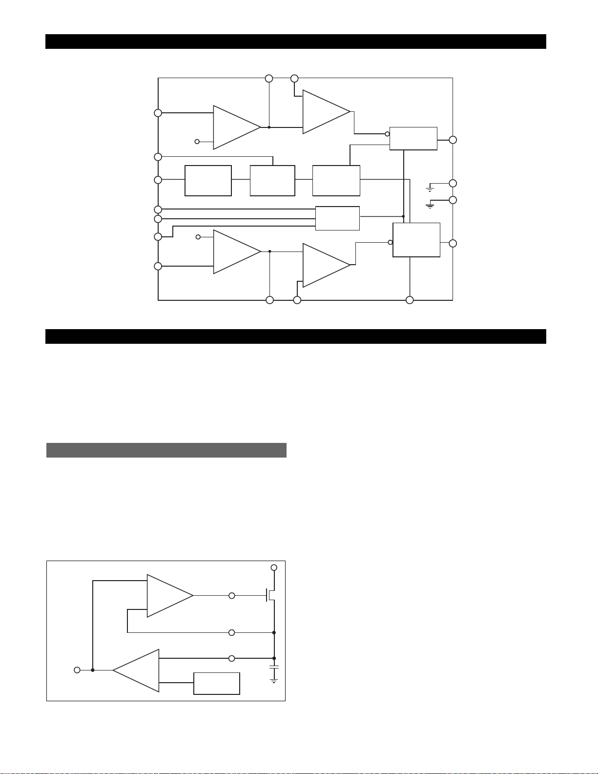
It is sometimes desirable to shift the switching noise spectrum to different frequencies. A pulse train applied to the
SYNC lead will terminate charging of the C
T
lead capacitor
and pull the CTlead voltage to ground for the duration of
the positive pulse level. This reduces the period of oscillation and increases the switching frequency.
Synchronization must always be done at a frequency
higher than the typical oscillator frequency. Using a lower
frequency will lead to erratic operation and poor regulation. The SYNC pulse train frequency should be at least 10
% higher than the unsynchronized oscillator frequency.
Synchronizing the oscillator will also decrease the maximum duty cycle. If the nominal oscillator frequency is
200kHz, increasing the oscillator frequency by 10% (to
220kHz) will decrease the maximum duty cycle from a
typical of 90% to about 89%. Increasing the frequency by
25% (to 250kHz) will change the maximum duty cycle to
about 87%. A 50% increase (to 300kHz) gives a maximum
duty cycle of about 85%. The width of the SYNC pulse
should be slightly shorter than the duration of the falling
edge of the CTlead waveform (see Figure 2a) so the SYNC
pulse doesnÕt interfere with the oscillator function.
Figure 2a: Sync pulse duration vs. CTlead discharge time.
The best way to determine if the pulse width is sufficiently
short is to examine the CTlead waveform with an oscilloscope. If Òdead spotsÓ are observed in the CTlead waveform,
decreasing the SYNC pulse width should be considered.
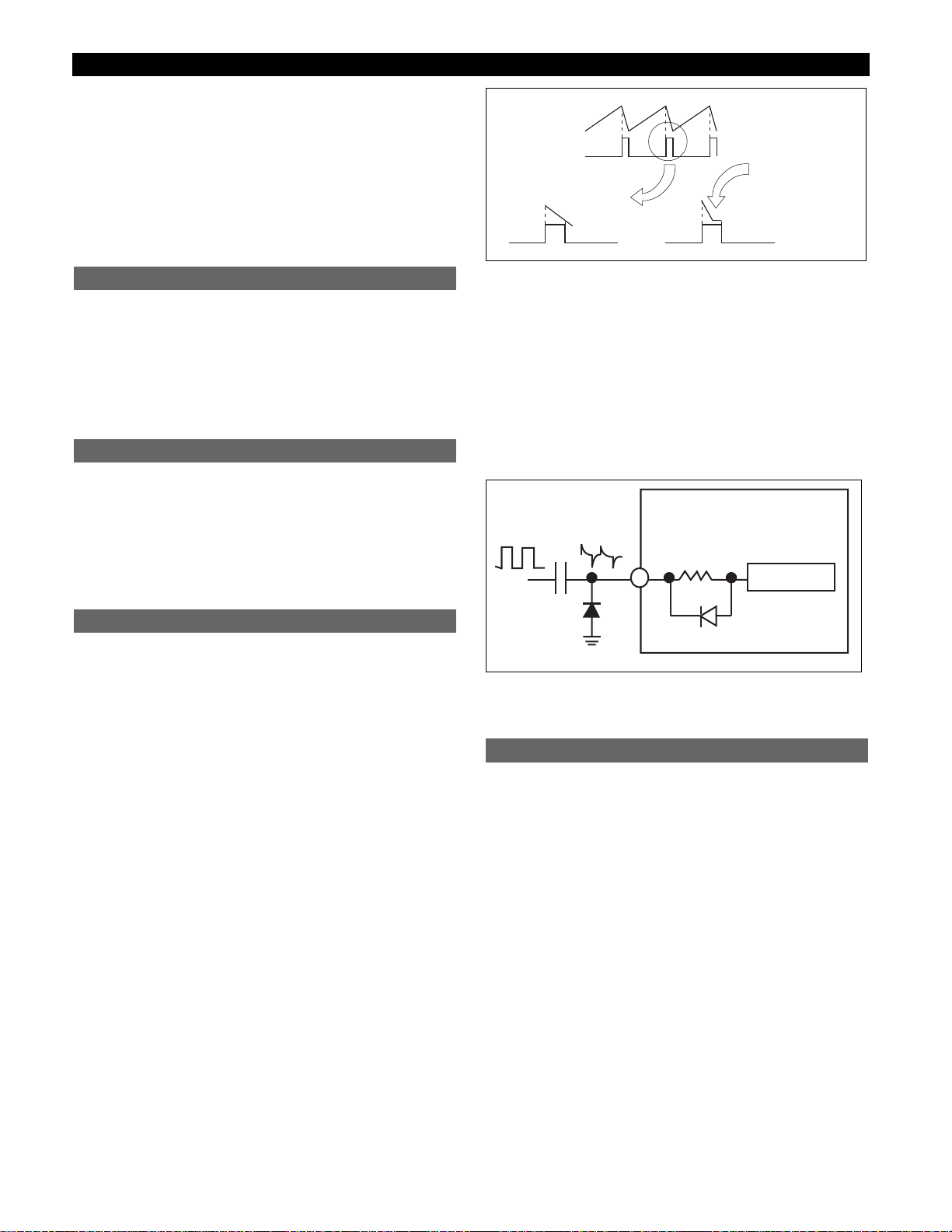
Alternatively, the SYNC signal may be AC coupled through
a small capacitor. In this case, care must be taken to ensure
that current pulled out of the IC during the high-to-low transition of the SYNC signal is limited to less than 5mA.
Figure 2b: Capacitive coupling of the SYNC signal. The external diode
is used to clamp the IC substrate diode if I
SYNC
is greater than 5mA
during the negative portion of the input waveform.
The CS5127 has no on-board current limit circuitry. An
example current limit circuit is provided in the Additional
Application Circuits section of this data sheet.
Overcurrent Protection
Sync Function
Constant Frequency
Voltage Mode Control
CT Lead Waveform
Sync Lead Waveform
If the sync pulse is longer
than the C
lead discharge
T
time, a short Òdead spotÓ
will exist during which the
output driver is off.
SYNC
Oscillator
20k
2200p
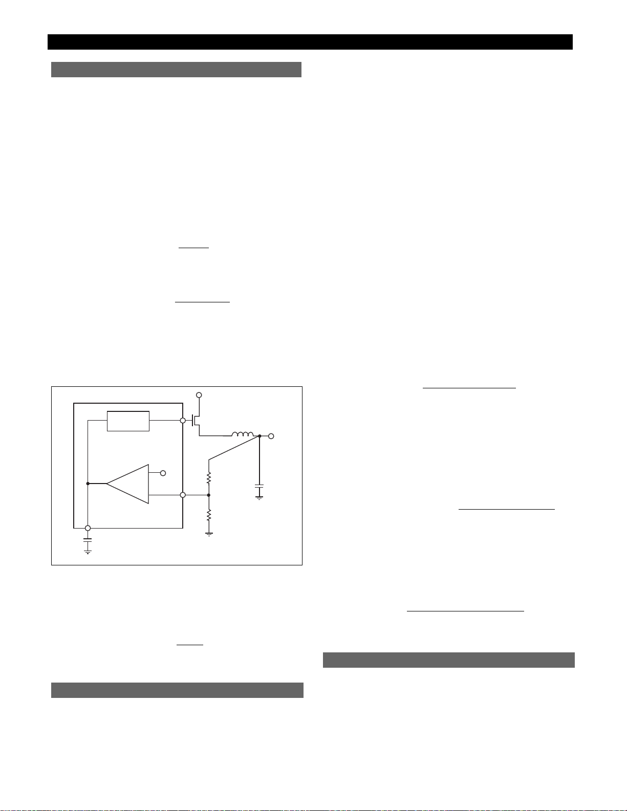
The feedback (V
FB)
leads are connected to external resistor
dividers to set the output voltage. The on-chip error amplifier is referenced to 1.275V, and the resistor divider values
are determined by selecting the desired output voltage
and the value of the divider resistor connected between
the VFBlead and ground.
Resistor R1 is chosen first based on a design trade-off of
system efficiency vs. output voltage accuracy. Low values
of divider resistance consume more current which decreases system efficiency. However, the VFBlead has a 1µA
maximum bias current which can introduce errors in the
output voltage if large resistance values are used. The
approximate value of current sinking through the resistor
divider is given by
I
V(FB)
=
The output voltage error that can be expected due to the
bias current is given by
Error Percentage = ´ 100%
where R1 is given in ohms. For example, setting R1 = 5K
yields an output voltage error of 0.39% while setting the
feedback divider current at 255µA. Larger currents will
result in reduced error.
Figure 3: Feedback resistor divider.
R2 can be sized according to the following formula once
the desired output voltage and the value of R1 have been
determined:
R2 = R1 -1
There are many factors to consider when choosing the
inductor. Maximum load current, core losses, winding
losses, output voltage ripple, short circuit current, saturation, component height, EMI/EMC and cost are all
variables the designer must consider. Inductance values
between 1µH and 50µH are suitable for use with the CS5127.
Low values within this range minimize the component size
and improve transient response, but larger values reduce
ripple current. Choosing the inductor value requires the
designer to make some choices early in the design. Output
current, output voltage and the input voltage range should
be known in order to make a good choice.
The input voltage range is bracketed by the maximum and
minimum expected values of V
IN
. Most computer applications use a fairly well-regulated supply with a typical
output voltage tolerance on the order of ±5%. The values
of V
IN(MAX)
and V
IN(MIN)
are used to calculate peak current
and minimum inductance value, respectively. However, if
the supply is well-regulated, these calculations may both
be made using the typical input voltage value with very
little error.
Current in the inductor while operating in the continuous
current mode (CCM) is defined as the load current plus
the inductor ripple current:
IL= I
OUT
+ I
RIPPLE
The ripple current waveform is triangular, and the current
is a function of the voltage across the inductor, the switch
on-time and the inductor value. Switch on-time is the duty
cycle divided by the operating frequency, and duty cycle
can be defined as the ratio of V
OUT
to VIN, such that
I
RIPPLE
=
The peak current can be described as the load current plus
half of the ripple current. Peak current must be less than
the maximum rated switch current. This limits the maximum load current that can be provided. It is also
important that the inductor can deliver the peak current
without saturating.
I
OUT(MAX)
= I
SWITCH(MAX)
-
Since the peak inductor current must be less than or equal
to the peak switch current, the minimum value of inductance can be calculated:
L
MIN
=
The theoretical limit on load current transient response is a
function of the inductor value, the load transient and the
voltage across the inductor. In conventionally-controlled
regulators, the actual limit is the time required by the control loop. Conventional current-mode and voltage-mode
control loops adjust the switch duty cycle over many oscillator periods, often requiring tens or even hundreds of
Load Current Transient Response
(V
IN(MIN)
- V
OUT)VOUT
f ´ V
IN(MIN)
´ I
SWITCH(MAX)
(V
IN(MAX)
- V
OUT)VOUT
2f ´ L ´ V
IN(MAX)
(VIN- V
OUT)VOUT
f ´ L ´ V
IN
Selecting the Inductor
)
V
OUT
1.275
(
(1E - 6) ´ R1
1.275
1.275V
R1
Selection of Feedback Lead Divider Resistor Values
CS5127
7
Applications Information
Output
Driver
V
1.275V
+
-
COMP
V
FB
GATE
R2
R1
OUT

CS5127
8
Applications Information: continued
microseconds to return to a steady-state. V
2
ª
control uses
the ripple voltage from the output capacitor and a ÒfastÓ
control loop to respond to load transients, with the result
that the transient response of the CS5127 is very close to
the theoretical limit. Response times are defined below.
t
RESPONSE(INCREASING)
=
t
RESPONSE(DECREASING)
=
Note that the response time to a load decrease is limited
only by the inductor value.
Inductor current rating is an important consideration. If
the regulated output is subject to short circuit or overcurrent conditions, the inductor must be sized to handle the
fault without damage. Sizing the inductor to handle fault
conditions within the maximum DC current rating helps to
ensure the coil doesnÕt overheat. Not only does this prevent damage to the inductor, but it reduces unwanted heat
generated by the system and makes thermal management
easier.
Selecting an open core inductor will minimize cost, but
EMI/EMC performance may be degraded. This is a tough
choice, since there are no guidelines to ensure these components will not prove troublesome.
Core materials influence the saturation current and saturation characteristics of the inductor. For example, a slightly
undersized inductor with a powdered iron core may provide satisfactory operation because powdered iron cores
have a ÒsoftÓ saturation curve compared to other core
materials.
Small physical size, low core losses and high temperature
operation will also increase cost. Finally, consider whether
an alternate supplier is an important consideration. All of
these factors can increase the cost of the inductor.
For light load designs, the CS5127 will operate in discontinuous current mode (DCM). In this regime, external
components can be smaller, since high power dissipation is
not an issue. In discontinuous mode, maximum output
current is defined as:
I
OUT(MAX)
=
where IPKis the maximum current allowed in the switch
FET.
Output capacitors are chosen primarily on the value of
equivalent series resistance, because this is what determines how much output ripple voltage will be present.
Most polarized capacitors appear resistive at the typical
oscillator frequencies of the CS5127. As a rule of thumb,
physically larger capacitors have lower ESR. The capacitorÕs value in µF is not of great importance, and values
from a few tens of µF to several hundreds of µF will work
well. Tantalum capacitors serve very well as output capacitors, despite their bad reputation for spectacular failure
due to excessive inrush current. This is not usually an issue
for output capacitors, because the failure is not associated
with discharge surges. Ripple current in the output capacitor is usually small enough that the ripple current rating is
not an issue. The ripple current waveform is triangular,
and the formula to calculate the ripple current value is:
I
RIPPLE
=
and output ripple voltage due to inductor ripple current is
given by:
V
RIPPLE(ESR)
=
A load step will produce an instantaneous change in
output voltage defined by the magnitude of the load step,
capacitor ESR and ESL.
DVO= (DIO´ ESD) + ESL
A good practice is to first choose the output capacitor to
accommodate voltage transient requirements and then to
choose the inductor value to provide an adequate ripple
voltage.
Increasing a capacitorÕs value typically reduces its ESR, but
there is a limit to how much improvement can be had. In
most applications, placing several smaller capacitors in
parallel will result in acceptable ESR while maintaining a
small PC board footprint. A warning is necessary at this
point. The V
2
ª
topology relies on the presence of some
amount of output ripple voltage being present to provide
the input signal for the ÒfastÓ control loop, and it is important that some ripple voltage be present at the lightest load
condition in normal operation to avoid subharmonic oscillation. Externally generated slope compensation can be
added to ensure proper operation.
The V
FFB
lead is tied to the PWM comparatorÕs non-inverting input, and provides the connection for the
externally-generated artificial ramp signal that is required
whenever duty cycle is greater than 50%.
Selecting the V
FFB
Lead Components
D
I
DT
(V
IN
- V
OUT
) ´ V
OUT
´ ESR
f ´ L ´ V
IN
(VIN- V
OUT)VOUT
f ´ L ´ V
IN
Selecting the Output Capacitor
(I
PK
)2f ´ L(VIN)
2V
OUT
´ (V
IN(MAX)
- V
OUT
)
Operating in Discontinuous Current Mode
Other Inductor Selection Concerns
L(ÆI
OUT
)
V
OUT
L(ÆI
OUT
)
(V
IN
- V
OUT
) ´ 0.85
 Loading...