

CHERRY Semiconductor CS5124, CS5126 Service Manual
V
CC
BIAS
UVLO
SS
Gnd
GATE
IS
V
FB
R8
0.39Ω
Q2
IRFR220
R5
17.4k
C2
1.5µF,
100V
C1
0.1µF,
100V
R2
200k
10µH
36-75V
IN
L1
R1
510k
Q1
ZVN3310A
T1
D1
MBRD360CT
R3
47Ω
R6
1k
C3
.022µF
C6
.01µF
R7
30.1k
C5
47µF,
10V
ISOLATED
RTN
5V
OUT
ENABLE
48VRTN
D4
R4
10Ω
BAS16LT1
C4
0.47µF,
25V
C8
1000pF
C7
0.1µF
TPS5908
U2
R9
10.0k
C9
1000pF
CS5124
CTX15-14514
Features
■ Line UVLO Monitoring
■ Low Current Sense
Voltage for Resistive
Current Sensing
■ External Synchronization
to Higher or Lower
Frequency Oscillator
(CS5126 Only)
■ Bias for Start up Circuitry
(CS5124 Only)
■ Thermal Shutdown
■ Sleep On/Off Pin
■ Soft Start Timer
■ Leading Edge Blanking
■ Direct Optocoupler
Interface
■ 90ns Propagation Delay
■ 35ns Driver Rise and Fall
Times
■ Sleep Mode
Package Options
CS5124/6
High Performance, Integrated Current Mode
PWM Controllers
CS5124/6
Description
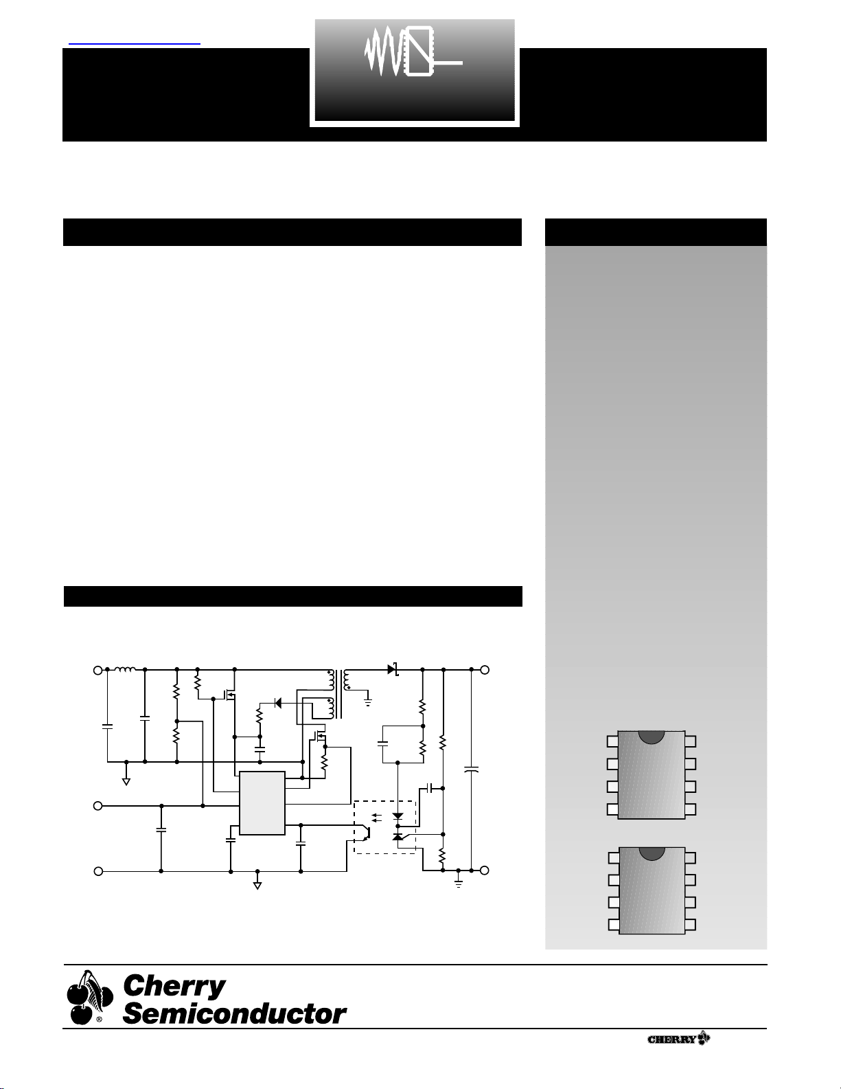
Applications Diagram
8 Lead SO Narrow
1
V
CC
BIAS
UVLO
SS
Gnd
GATE
I
SENSE
V
FB
Cherry Semiconductor Corporation
2000 South County Trail, East Greenwich, RI 02818
Tel: (401)885-3600 Fax: (401)885-5786
Email: info@cherry-semi.com
Web Site: www.cherry-semi.com
A Company
®
Rev. 3/12/99
Gnd
UVLO
V
CC
SYNC
SS
GATE
I
SENSE
V
FB
CS5124
CS5126
48V to 5V, 1A flyback converter using the CS5124
The CS5124/6 is a fixed frequency
current mode controller designed
specifically for DC-DC converters
found in the telecommunications
industry. The CS5124/6 integrates
many commonly required current
mode power supply features and
allows the power supply designer to
realize substantial cost and board
space savings. The product matrix is
as follows:
CS5124: 400kHz w/V
BIAS
Pin,
195mV first current sense threshold
CS5126: 200kHz w/SYNC Pin,
335mV first current sense threshold
The CS5124/6 integrates the following features: Internal Oscillator, Slope
Compensation, Sleep On/Off, Under
Voltage Lock Out, Thermal
Shutdown, Soft Start Timer, Low
Voltage Current Sense for Resistive
Sensing, Second Current Threshold
for Pulse by Pulse Over Current
Protection, a Direct Optocoupler
Interface and Leading Edge Current
Blanking.
The CS5124/6 has supply range of
7.7V to 20V and is available in 8 pin
SO narrow package.
查询CS5124供应商
1
1
Pin Symbol Lead Name
V
MAX
V
MIN
I
SOURCE
I
SINK
V
CC
VCCPower Input 20V -0.3V 1mA 1.5A Peak
200mA DC
SYNC (CS5126) Clock Synchronization Input 20V -0.3V 1mA 1mA
V
BIAS
(CS5124) VCCClamp Output 20V -0.3V 1mA 1mA
UVLO UVLO Shutdown Input 6V -0.3V 1mA 1mA
SS Soft Start Capacitor Input 6V -0.3V 1mA 2mA
V
FB
Voltage Feed Back Input 6V -0.3V 3mA 20mA
I
SENSE
Current Sense Input 6V -0.3V 1mA 1mA
GROUND Ground 0V 0V 1.5A peak 1mA
200mA DC
GATE Gate Drive Output 20V -0.3V 1.5A Peak 1.5A Peak
200mA DC 200mA DC
Operating Junction Temperature, T
J
. . . . . . . . . . . . . . . . . . . . . . . . . . . . . . . . . . . . . . . . . . . . . . . . . . . . . . . . . . . . . . .-40 to 135°C
Storage Temperature Range, TS . . . . . . . . . . . . . . . . . . . . . . . . . . . . . . . . . . . . . . . . . . . . . . . . . . . . . . . . . . . . . . . . . . .-40 to 150°C
ESD (Human Body Model) . . . . . . . . . . . . . . . . . . . . . . . . . . . . . . . . . . . . . . . . . . . . . . . . . . . . . . . . . . . . . . . . . . . . . . . . . . . . . .2kV
ESD (Machine Model) . . . . . . . . . . . . . . . . . . . . . . . . . . . . . . . . . . . . . . . . . . . . . . . . . . . . . . . . . . . . . . . . . . . . . . . . . . . . . . . . .200V
Lead Temperature Soldering:
Reflow (SMD styles only) . . . . . . . . . . . . . . . . . . . . . . . . . . . . . . . . . . . . . . . . . . . . . . . . . .60 sec. max above 183°C, 230°C peak
CS5124/6
2
Absolute Maximum Ratings
PARAMETER TEST CONDITIONS MIN TYP MAX UNIT
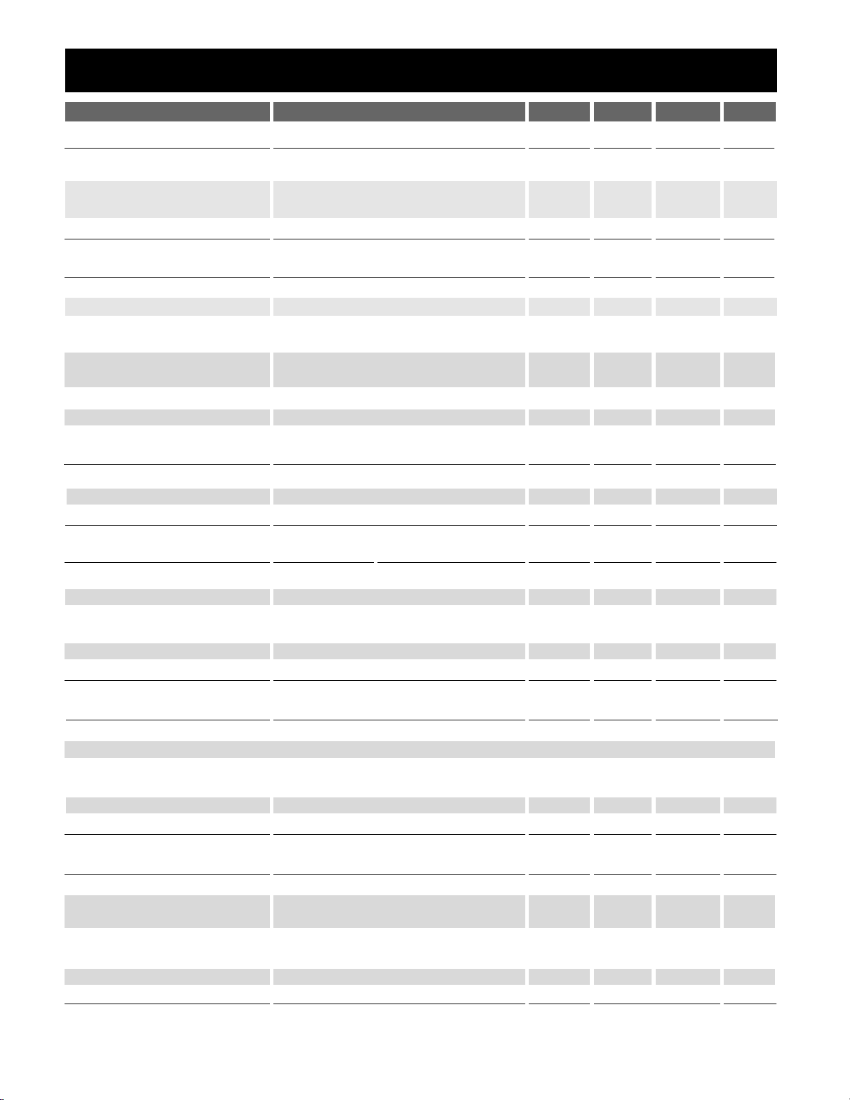
Electrical Characteristics: -40°C ≤ TJ ≤ 125°C, -40°C ≤ TA ≤ 105°C, 7.60V ≤ V
CC
≤ 20V, UVLO = 3.0V, I
SENSE
= 0V,
C
V(CC)
= 0.33µF, C
GATE
= 1nF (ESR = 10Ω), CSS= 470pF C
V(FB)
= 100pF, unless otherwise stated.
■ General
ICCOperating - V
GATE
not switching. 10 13 mA
ICCat VCCLow VCC= 6V 500 750 µA
ICCSleep V
UVL
= 1V 210 275 µA
■ Low V
CC
Lockout
VCCTurn-on Threshold Voltage 7.2 7.7 8.3 V
VCCTurn-off Threshold Voltage 6.8 7.3 7.8 V
VCCHysteresis 350 425 500 mV
■ UVLO
Sleep Threshold Voltage UVLO decreasing 1.5 1.8 2.3 V
Sleep Threshold Voltage UVLO increasing 1.88 2.45 V
Sleep Hysteresis 35 85 150 mV
UVLO Turn-off (Note 1) 2.3 2.45 2.6 V
Threshold Voltage
UVLO Turn-on (Note 1) 2.50 2.63 2.76 V
Threshold Voltage
UVLO Hysteresis Turn-on – Turnoff (-40°C ≤ TJ≤ 100°C) 170 185 200 mV
(Note 1)
UVLO Hysteresis Turn-on – Turnoff (100°C ≤ TJ≤ 125°C) 50 185 400 mV
(Note 1)
UVLO Input Bias Current -1 1 µA
UVLO Clamp With UVLO sinking 1mA. 5 7.5 12 V
CS5124/6
3
Electrical Characteristics: -40°C ≤ TJ ≤ 125°C, -40°C ≤ TA ≤ 105°C, 7.60V ≤ V
CC
≤ 20V, UVLO = 3.0V, I
SENSE
= 0V,
C
V(CC)
= 0.33µF, C
GATE
= 1nF (ESR = 10Ω), CSS= 470pF C
V(FB)
= 100pF, unless otherwise stated.
PARAMETER TEST CONDITIONS MIN TYP MAX UNIT
■ V
CC
Clamp and BIAS Pin CS5124 Only. Connect an NFET as follows: BIAS = G, VCC= S, V
IN
= D.
VCCClamp Voltage 36V ≤ VIN≤ 60V, 220nF ≤ 7.275 7.9 8.625 V
CSS≤ 500nF, R = 500k
BIAS Minimum Voltage Measure Voltage on BIAS with: 1.6 2.8 4 V
10V ≤ VCC≤ 20V and 50µA ≤ I
BIAS
≤ 1mA
BIAS Clamp With BIAS pin sinking 1mA 12 15 20 V
■ 200kHz Oscillator CS5126 Only
Operating Frequency 175 200 225 kHz
Max Duty Cycle Clamp 78 82.5 85 %
Slope Compensation 12 18 23 mV/µs
(Normal operation)
Slope Compensation
(Synchronized operation) (Note 1) 7 12 16 mV/µs
SYNC Input Threshold Voltage 1 2 3 V
SYNC Input Impedance Measured with SYNC = 1V &10V 50 120 230 kΩ
■ 400kHz Oscillator CS5124 Only
Operating Frequency 360 400 440 kHz
Max Duty Cycle Clamp 80.0 82.5 85.0 %
Slope Compensation 15 21 26 mV/µs
■ Soft Start
Soft Start Charge Current 7 10 13 µA
Soft Start Discharge Current 0.5 10.0 mA
VSSVoltage when V
FB
V
FB
= 300mV 1.40 1.62 1.80 V
Begins to Rise
Peak Soft Start Charge Voltage 4.7 4.9 V
Valley Soft Start Discharge Voltage 200 275 400 mV
■ Current Sense CS5124 Only
First Current Sense Threshold At max duty cycle. 170 195 215 mV
Second Current Sense Threshold 250 275 315 mV
I
SENSE
to GATE Prop. Delay 0 to 700mV pulse into I
SENSE
60 90 130 ns
(after blanking time)
Leading Edge Blanking Time 0 to 400mV pulse into I
SENSE
90 130 180 ns
Internal Offset (Note 1) 60 mV
■ Current Sense CS5126 Only
First Current Sense Threshold At max duty cycle 300 335 360 mV
Second Current Sense 485 525 575 mV
Threshold
I
SENSE
to GATE Prop. Delay 0 to 800mV pulse into I
SENSE
60 90 130 ns
(after blanking time)
Leading Edge Blanking Time 0 to 550mV pulse into I
SENSE
110 175 210 ns
Internal Offset (Note 1) 125 mV
 Loading...