

CHERRY Semiconductor CS5106 Service Manual
Features
■ Programmable Fixed
Frequency
■ Programmable FET Non-
overlap
■ Enable Lead
■ 12V Fixed Auxiliary
Supply Control
■ Under and Overvoltage
Shutdown
■ Output Undervoltage
Protection with Timer
■ Master/Slave Clock
Syncing Capability
■ Sync Frequency Range
Detection
■ 80ns PWM Propagation
Delay
■ 20mA 5V Reference
Output
■ Small 24 lead SSOP
Package
■ Controlled Hiccup Mode
Package Options
CS5106
Multi-Feature, Synchronous plus Auxiliary
PWM Controller
CS5106
Description
The CS5106 is a fixed frequency,
current mode controller with one
single NFET driver and one dual
FET, synchronous driver. The synchronous driver allows for
increased efficiency of the main isolated power stage and the single
driver allows the designer to develop auxiliary supplies for controller
power as well as secondary side
house keeping. In addition,
because the synchronous drivers
have programmable FET non-overlap, the CS5106 is an ideal controller for soft-switched converter
topologies.
The CS5106 is specifically designed
for isolated topologies where speed,
flexibility, reduced size and
reduced component count are
requirements. The controller contains the following features:
Undervoltage Shutdown,
Overvoltage Shutdown,
Programmable Frequency,
Programmable Synchronous NonOverlap Time, Master/Slave
Clocking with Frequency Range
Detection, Enable, Output
Undervoltage Protection with
Timer, 20mA 5V Output, 80ns
PWM propagation delay, and
Controlled Hiccup Mode.
The CS5106 has junction temperature and supply ranges of -40ûC to
125ûC and 9V to 16V respectively
and is available in the 24 lead SSOP
package.
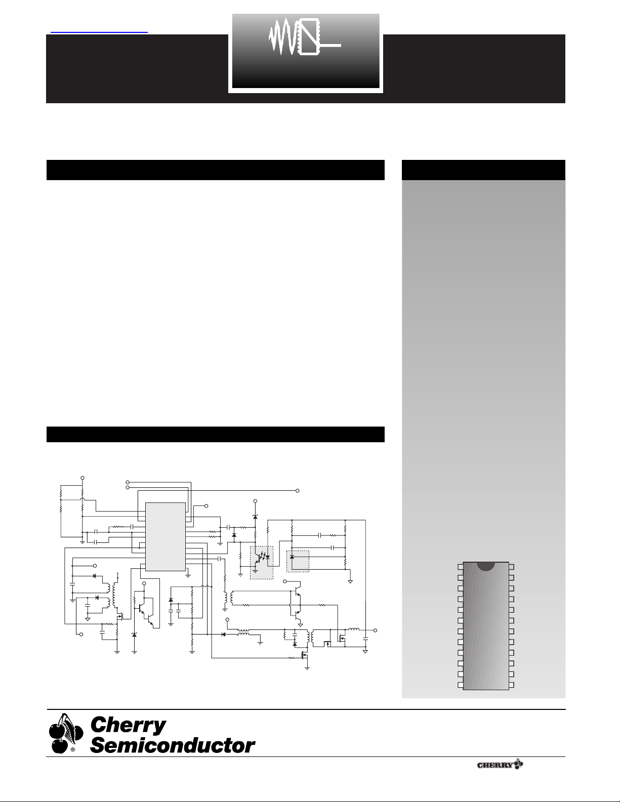
Applications Diagram
24 Lead SSOP
1
UVSD
OVSD
OAM
OAOUT
V
5REF
OUVDELAY
I
LIM1
RAMP1
V
FB1
V
SS
V
CC
GATE1
ENABLE
PROGRAM
SYNC
IN
SYNC
OUT
FADJ
DLYSET
I
LIM2
RAMP2
V
FB2
V
DD
GATE2B
GATE2
Rev. 10/27/98
48V to 3.3V Forward Converter with Synchronous Rectifiers
Cherry Semiconductor Corporation
2000 South County Trail, East Greenwich, RI 02818
Tel: (401)885-3600 Fax: (401)885-5786
Email: info@cherry-semi.com
Web Site: www.cherry-semi.com
A Company
¨
查询CS5106供应商
V
IN
C5
V
C1
C2
V
D1
D2
AUXS
SYNC
ENABLE
R4
AUXP
V
T1
R5
C7
IN
CS5106
UVSD
ENABLE
PROGRAM
OVSD
V
SYNC
5REF
C3
IN
V
R8
Q1
R6
IN
D6
OAM
OA
OUVDELAY
I
LIM1
RAMP1
V
V
V
GATE1
Q2
SYNC
OUT
FADJ
OUT
DLYSET
I
LIM2
RAMP2
V
FB1
FB2
GATE2B
SS
GATE2
CC
V
D3
C10
C9
R27
R1
R2
R3
C4
V
R13
AUXP
OUT
D5
C6
R7
R20
R15
D8
R14
C8
CNY17-4
T4
R26
V
IN
T3
D4
R23
SYNC
IN
R24
R25
DD
R9
R10
R11
R12
V
5REF
R21
R18
R17
C13
R19
L1
Q5
Q4
R16
C14
TL431
V
AUXS
Q7
Q6
T2
C11
D7
Q3
R22
V
MAIN
C12
1

CS5106
2
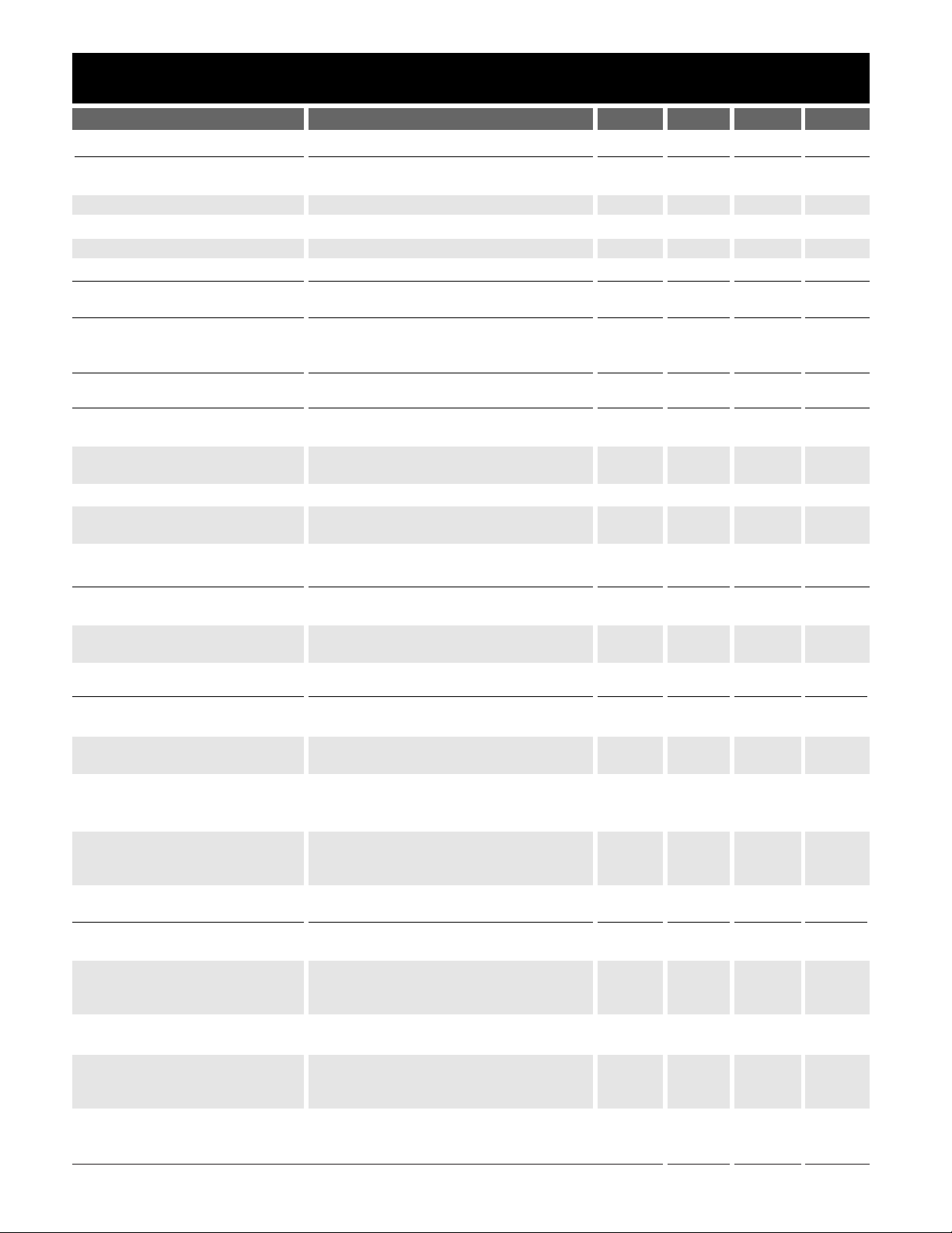
Absolute Maximum Ratings
Lead Symbol Lead Name
V
MAX
V
MIN
I
SOURCE
I
SINK
UVSD Undervoltage Shutdown Input 6V -0.3V 1mA N/A
OVSD Overvoltage Shutdown Input 6V -0.3V 1mA N/A
V
5REF
5V Reference Output 6V -0.3V 150mA 25mA
OAM Error Amp Minus Input 6V -0.3V 250µA 1.2mA
OAOUT Error Amp Output 6V -0.3V 300µA 100mA
OUVDELAY Output Overcurrent Timer Capacitor 6V -0.3V 15µA N/A
I
LIM1
Auxiliary Primary Side Current Limit Input 6V -0.3V 10µA N/A
RAMP1 Auxiliary Primary Side Current Ramp Input 6V -0.3V 10µA N/A
V
FB1
Auxiliary Voltage Feedback Input 6V -0.3V 5µA 100µA
V
SS
Bootstrapped Power Input 20V -0.3V 2µA 0.5A Peak
300mA DC
V
CC
Main Power Input 20V -0.3V See Note 1 0.5A Peak
300mA DC
GATE1 Auxiliary FET Driver Output 20V -0.3V 0.5A Peak 0.5Peak
100mA DC 100mA DC
Gnd Ground 0V 0V 0.5A Peak N/A
300mA DC
GATE2 Synchronous FET Driver Output 20V -0.3V 0.5A Peak 0.5APeak
100mA DC 100mA DC
GATE2B Synchronous FET Driver Output B 20V -0.3V 0.5A Peak 0.5A Peak
100mA DC 100mA DC
V
FB2
Synchronous Voltage Feedback Input 6V -0.3V 10µA 100µA
RAMP2 Synchronous Primary Side Current Ramp Input 6V -0.3V 10µA N/A
I
LIM2
Synchronous Primary Side Current Limit Input 6V -0.3V 10µA N/A
DLYSET Gate Non-Overlap Programming Input 2.5V -0.3V 125µA N/A
FADJ Frequency Programming Input 2.5V -0.3V 125µA N/A
SYNC
OUT
Clock Master Output 6V -0.3V 50mA 100mA
SYNC
IN
Clock Slave Input 6V -0.3V N/A 1mA
PROGRAM Enable Programming Input 16V -0.3V 30µA N/A
ENABLE Enable Input 16V -0.3V 300µA N/A
Note 1: Current out of V
CC
is not limited. Care should be taken to prevent shorting VCCto Ground.
Operating Junction Temperature, TJ..................................................................................................................................... 150¡C
Operating Temperature Range, TA...............................................................................................................................-40 to 85¡C
Storage Temperature Range, TS...................................................................................................................................-65 to 150¡C
ESD (Human Body Model).........................................................................................................................................................2kV
Lead Temperature Soldering: Reflow (SMD styles only).............................................60 sec. max above 183¡C, 230¡C peak

CS5106
3
PARAMETER TEST CONDITIONS MIN TYP MAX UNIT
Electrical Characteristics: TJ = -40¡C to 125¡C, V
SS
= 9 to 16V, V
5REFILOAD
= 2mA, SYNC
OUT
Free Running, unless other-
wise specified. For All Specs: UVSD=6V, OVSD = 0V, ENABLE = 0V, I
LIM(1,2)
= 0,V
FB(1,2)
= 3V,R
FADJ
= R
DLYSET
= 27.4k½.
■ V
SS
Supply Current Measure current into VSSwhen 16.00 23.00 mA
V
5REFILOAD
=0mA. 9V ² VSS² 13V.
Measure current into VSSwhen 16.00 25.00 mA
V
5REFILOAD
=0mA. 13V < VSS² 16V.
Measure current into VSSwhen 16.00 30.00 mA
V
5REFILOAD
=0mA. 16V < VSS² 20V.
■ Low V
CC
Supply Current Float VSS. Set VCC=7V & measure 1.50 3.50 mA
VCCcurrent while V
5REFILOAD
=0mA.
■ V
SS
TO VCCDIODE
Diode ON Voltage Measure VSS- VCC. 0.20 0.75 1.00 V
■ Reference
5V Internal Voltage Reference Measure V
REF
voltage when 4.85 5.00 5.15 V
I
REF
=0 and I
REF
=20 mA.
V
REF
OK Threshold Adjust V
REF
from 4.8V-4.0V until 4.30 4.55 4.70 V
PWM1,2 goes low.
■ Low V
CC
Lockout
VCCTurnon Threshold Voltage VCCincreasing until ICC> 3.5mA 7.00 7.25 7.50 V
V
5REFILOAD
= 0mA
VCCTurnoff Threshold Voltage VCCdecreasing until ICC< 3.5mA 6.30 6.70 7.10 V
V
5REFILOAD
= 0mA
Hysteresis Turnon - Turnoff 0.40 0.55 0.70 V
■ Clock
Operating Frequency1 Measure frequency from SYNC
OUT
. 485.0 512.0 540.0 kHz
SYNCINInput Impedance Measure input impedance. 7.00 15.00 k½
SYNC
OUT
Output Low Voltage R
LOAD
= 2k½ to V
5REF
1.00 1.50 V
SYNC
OUT
Output High R
LOAD
= 2k½ to Gnd 3.50 4.20 V
Voltage
SYNCINDetect Frequency Verify SYNC
OUT
= SYNCIN, 425.0 555.0 kHz
R
LOAD
= 2k½ to Gnd
Max. Low SYNC Rej. Frequency Verify SYNC
OUT
= FCLK when 340.0 kHz
R
LOAD
= 2k½ to Gnd.
Min. High SYNC Rej. Frequency Verify SYNC
OUT
= FCLK when 690 kHz
R
LOAD
= 2k½ to Gnd.
SYNCINInput Threshold Functional Testing 0.90 1.85 2.90 V
Voltage Verify FCLK from 1.0V to 2.8V.
Main PWM Clock Pulse (GBD) - CLPH1
Width One Shot Pulse Width 80.0 100.0 120.0 ns
Aux PWM Clock Pulse (GBD) -CLPH2
Width One Shot Pulse Width 80.0 100.0 120.0 ns
■ Bias Supply Error Amplifier
Output Low Voltage V
SS
> 12.6V. Measure OAOUT 43.0 85.0 mV
voltage when sinking 1.0 mA.
Output High Voltage V
SS
< 11.4V. Measure OAOUT 4.55 4.75 V
voltage when sourcing 150µA.
Output High Source Current V
SS
< 11.4V. Measure OAOUT source 150.0 225.0 300.0 µA
current when OAOUT = 0.5V.
CS5106
4
PARAMETER TEST CONDITIONS MIN TYP MAX UNIT
Electrical Characteristics: TJ = -40¡C to 125¡C, V
SS
= 9 to 16V, V
5REFILOAD
= 2mA, SYNC
OUT
Free Running, unless other-
wise specified. For All Specs: UVSD=6V, OVSD = 0V, ENABLE = 0V, I
LIM(1,2)
= 0,V
FB(1,2)
= 3V,R
FADJ
= R
DLYSET
= 27.4k½.
■ Bias Supply Error Amplifier: continued
Output Low Sink Current V
SS
> 12.6V. Measure OAOUT sink 3.0 20.0 50.0 mA
current when OAOUT = 2.5V.
VSSSet Point Adjust VSSuntil OAOUT goes low. 11.60 12.25 12.80 V
Large Signal Gain (GBD) 15.00 V/mV
Unity Gain Bandwidth (GBD) 1.00 MHz
Common Mode Input Range (GBD) 1.00 2.00 V
■ V
SS
Voltage
VSSReset Voltage Toggle ENABLE between Gnd & VCC,
then adjust VSSfrom 2.0V-0.8V until
OAOUT goes high. 1.00 1.40 1.80 V
■ Undervoltage Lockout
UVSD Turn On Adjust UVSD from 4.7V-5.3V 4.80 5.00 5.10 V
Threshold Voltage until GATE 1, 2 goes high.
UVSD Turn Off Threshold Adjust UVSD from 5.1V-4.3V 4.45 4.70 4.95 V
Voltage until GATE 1, 2 goes low.
Hysteresis Turnon - Turnoff 0.20 0.27 0.40 V
UVSD Input Bias Current Set UVSD=0V. Measure Current 0.20 0.50 µA
out of UVSD lead.
■ Overvoltage Lockout
OVSD Threshold Voltage Adjust OVSD from 4.7V-5.3V 4.85 5.00 5.15 V
until GATE 1, 2 goes low.
OVSD Input Bias Current Set OVSD=0V. Measure Current out 0.20 0.50 µA
of OVSD lead.
■ ENABLE & PROGRAM
ENABLE Lead Output Current Measure current out of 100.0 266.0 500.0 µA
ENABLE when ENABLE = 0V.
PROGRAM Lead Output Measure current out of 20.0 60.0 100.0 µA
Current PROGRAM when PROGRAM = 0V.
PROGRAM Threshold ENABLE = Gnd. Adjust 1.20 1.40 1.60 V
Voltage PROGRAM from 1.0V - 1.8V
until GATE 1, 2 goes high.
ENABLE Threshold Voltage PROGRAM = Gnd. 1.20 1.40 1.60 V
Adjust ENABLE from 1.0V - 1.8V
until GATE 1, 2 goes high.
■ Output Undervoltage Delay
OUVDELAY Charging Set OUVDELAY = 1V, V
FB1
= 4.4V 7.50 10.00 12.50 µA
Current Measure OUVDELAY I
CHARGE
.
OUVDELAY Latchoff Voltage Toggle ENABLE between Gnd & VCC, 4.80 5.00 5.20 V
then adjust OUVDELAY from
4.7V - 5.3V until GATE 1, 2, goes low.
OUVDELAY Set Current OUVDELAY = VOCLO + 50mV 0.50 1.00 mA
Measure current into OUVDELAY.
V
FB1
Charge Threshold VSS=1V. Toggle ENABLE between 4.05 4.22 4.40 V
Gnd & VCC, adjust V
FB1
from 3.8V - 4.6V
until GATE 1, 2 goes low.
V
FB2
Charge Threshold V
SS
= 1V. Toggle ENABLE between 3.90 4.15 4.35 V
Gnd & VCC, adjust V
FB2
from 3.8V - 4.6V
until GATE 1, 2 goes low.
 Loading...