

Cherry Semiconductor CS51033YN8, CS51033YDR8, CS51033YD8 Datasheet
1
Features
■ 1A Totem Pole Output
Driver
■ High Speed Oscillator
(700kHz max)
■ No Stability
Compensation Required
■ Lossless Short Circuit
Protection
■ 2% Precision Reference
■ Programmable Soft Start
Package Options
CS51033
Fast PFET Buck Controller
Does Not Require Compensation
CS51033
Description
The CS51033 is a switching controller for use in DC-DC converters.
It can be used in the buck topology
with a minimum number of external components. The CS51033 consists of a 1.0A power driver for controlling the gate of a discrete Pchannel transistor, fixed frequency
oscillator, short circuit protection
timer, programmable soft start, precision reference, fast output voltage
monitoring comparator, and output
stage driver logic with latch.
The high frequency oscillator
allows the use of small inductors
and output capacitors, minimizing
PC board area and systems cost.
The programmable soft start
reduces current surges at start up.
The short circuit protection timer
significantly reduces the PFET duty
cycle to approximately 1/30 of its
normal cycle during short circuit
conditions.
The CS51033 is available in 8L SO
and 8L PDIP plastic packages.
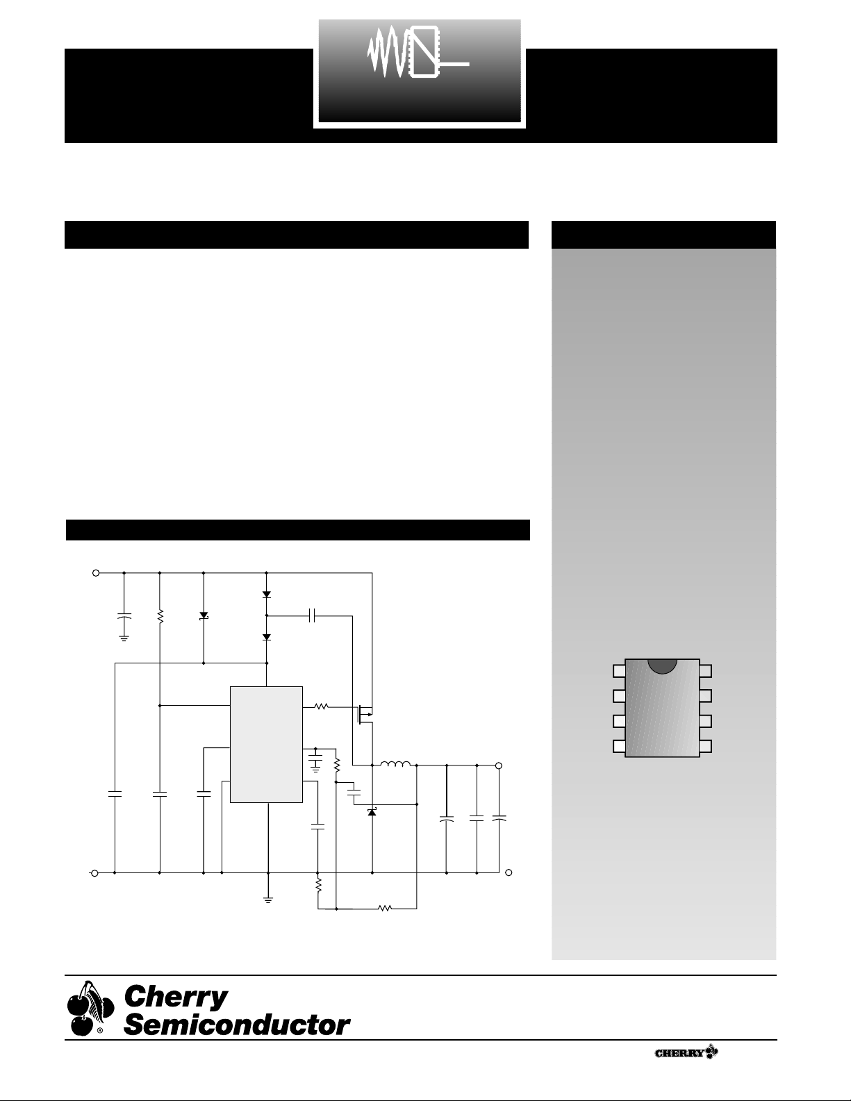
Typical Application Diagram
V
GATE
PGnd
C
OSC
Gnd
V
C
CS
V
CC
V
FB
8 Lead SO Narrow & PDIP
A Company
®
Rev. 2/13/98
Cherry Semiconductor Corporation
2000 South County Trail, East Greenwich, RI 02818
Tel: (401)885-3600 Fax: (401)885-5786
Email: info@cherry-semi.com
Web Site: www.cherry-semi.com
3.3V
IN
100µF
C
1µF
C
IN
R
C
10Ω
C
100µF
3
2
D
2
1N4148
1N4148
V
CC
C
OSC
Gnd
D
3
CS51033
PGnd
1N5818
C
OSC
150pF
D
4
C
1
0.1µF
R
V
FB
CS
0.1µF
CS
10Ω
0.01µF
G
IRF 7404
4.7µH
100
.1µF
D
1
1N5821
C
100µF
V
U1
C
V
GATE
1.5V
OUT
@3Amp
C
4
0
0.1µF
100µF
1
Gnd
NOTE: Capacitors C
caps used for noise reduction.
, C3 and C4 are low ESR tantalum
2
1.5k
R
A
300
R
B
Gnd
Power Supply Voltage, VCC..........................................................................................................................................................5V
Driver Supply Voltage, V
C
..........................................................................................................................................................20V
Driver Output Voltage, V
GATE
...................................................................................................................................................20V
C
OSC
, CS, VFB(Logic Pins) ............................................................................................................................................................5V
Peak Output Current................................................................................................................................................................. 1.0A
Steady State Output Current ................................................................................................................................................200mA
Operating Junction Temperature, TJ..................................................................................................................................... 150°C
Storage Temperature Range, TS...................................................................................................................................-65 to 150°C
ESD (Human Body Model).........................................................................................................................................................2kV
Lead Temperature Soldering
Wave Solder (through hole styles only) .....................................................................................10 sec. max, 260°C peak
Reflow (SMD styles only) ......................................................................................60 sec. max above 183°C, 230°C peak
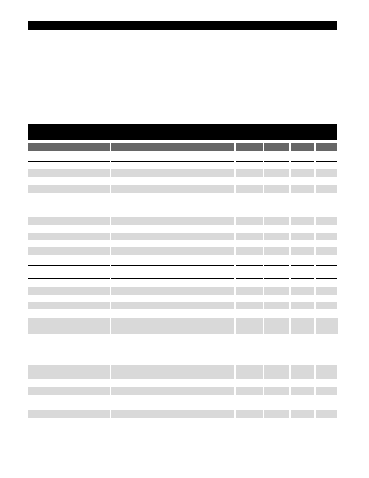
PARAMETER TEST CONDITIONS MIN TYP MAX UNIT
2
CS51033
Absolute Maximum Ratings
Electrical Characteristics: Specifications apply for 3.135 ≤ VCC≤ 3.465V, 3V ≤ VC≤ 16V,
-40°C ≤ TA≤ 125°C, -40°C ≤ TJ≤ 125°C, unless otherwise specified.
■ Oscillator V
FB
= 1.2V
Frequency C
OSC
= 470pF 160 200 240 kHz
Charge Current 1.4V < V
COSC
< 2V 110 µA
Discharge Current 2.7V > V
COSC
> 2V 660 µA
Maximum Duty Cycle 1 – (t
OFF/tON
) 80.0 83.3 %
■ Short Circuit Timer V
FB
= 1.0V; CS = 0.1µF; V
COSC
= 2V
Charge Current 1V < V
CS
< 2V 175 264 325 µA
Fast Discharge Current 2.55V > V
CS
> 2.4V 40 66 80 µA
Slow Discharge Current 2.4V > V
CS
> 1.5V 4 6 10 µA
Start Fault Inhibit Time 0.70 0.85 1.40 ms
Valid Fault Time 2.6V > V
CS
> 2.4V 0.2 0.3 0.45 ms
GATE Inhibit Time 2.4V > V
CS
> 1.5V 9 15 23 ms
Duty Cycle 2.5 3.1 4.6 %
■ CS Comparator V
FB
= 1V
Fault Enable CS Voltage 2.5 V
Max. CS Voltage VFB= 1.5V 2.6 V
Fault Detect Voltage VCSwhen GATE goes high 2.4 V
Fault Inhibit Voltage Minimum V
CS
1.5 V
Hold Off Release Voltage V
FB
= 0V 0.4 0.7 1.0 V
Regulator Threshold V
CS
= 1.5V 0.725 0.866 1.035 V
Voltage Clamp
■ V
FB
Comparator V
COSC
= VCS= 2V
Regulator Threshold Voltage TJ= 25°C (Note 1) 1.225 1.250 1.275 V
TJ= -40 to 125°C 1.210 1.250 1.290 V
Fault Threshold Voltage TJ= 25°C (Note 1) 1.12 1.15 1.17 V
TJ= -40 to 125°C 1.10 1.15 1.19 V
Threshold Line Regulation 3.135V ≤ VCC≤ 3.465 6 15 mV
Input Bias Current VFB= 0V 1 4 µA
Voltage Tracking (Regulator Threshold Voltage - 70 100 120 mV
Fault Threshold Voltage)
Input Hysteresis Voltage 4 20 mV

PARAMETER TEST CONDITIONS MIN TYP MAX UNIT
CS51033
3
Package Pin Description
PACKAGE PIN # PIN SYMBOL FUNCTION
Electrical Characteristics: Specifications apply for 3.135 ≤ VCC≤ 3.465V, 3V ≤ VC≤ 16V,
-40°C ≤ TJ≤ 125°C, unless otherwise specified.
8L SO Narrow & PDIP
1V
GATE
Driver pin to gate of external PFET.
2 PGnd Output power stage ground connection.
3C
OSC
Oscillator frequency programming capacitor.
4 Gnd Logic ground.
5V
FB
Feedback voltage input.
6V
CC
Logic supply voltage.
7 CS Soft start and fault timing capacitor.
8V
C
Driver supply voltage.
■ Power Stage V
C
= 10V; VFB= 1.2V
GATE DC Low Saturation V
COSC
= 1V; 200mA Sink 1.2 1.5 V
Voltage
GATE DC High Saturation V
COSC
= 2.7V; 200mA Source; VC= V
GATE
1.5 2.1 V
Voltage
Rise Time C
GATE
= 1nF; 1.5V < V
GATE
< 9V 25 60 ns
Fall Time C
GATE
= 1nF; 9V > V
GATE
> 1.5V 25 60 ns
■ Current Drain
I
CC
3.135V < VCC< 3.465V, Gate switching 3.5 6.0 mA
I
C
3V < VC< 16V, Gate non-switching 2.7 4.0 mA
Note1: Guaranteed by design not 100% tested in production.
 Loading...